

Datasheet P87C592EFA-02, P80C592FHA-00, P80C592FFA-00, P87C592EFL-02, P87C592EFA-A2 Datasheet (Philips)
Page 1

DATA SH EET
Product specification
Supersedes data of January 1995
File under Integrated Circuits, IC18
1996 Jun 27
INTEGRATED CIRCUITS
P8xC592
8-bit microcontroller
with on-chip CAN
Page 2

1996 Jun 27 2
Philips Semiconductors Product specification
8-bit microcontroller with on-chip CAN P8xC592
CONTENTS
1 FEATURES
2 GENERAL DESCRIPTION
3 ORDERING INFORMATION
4 BLOCK DIAGRAM
5 PINNING
6 FUNCTIONAL DESCRIPTION
7 MEMORY ORGANIZATION
7.1 Program Memory
7.2 Internal Data Memory
7.3 External Data Memory
8 I/O PORT STRUCTURE
9 PULSE WIDTH MODULATED OUTPUTS
(PWM)
9.1 Prescaler frequency control register (PWMP)
9.2 Pulse Width Register 0 (PWM0)
9.3 Pulse Width Register 1 (PWM1)
10 ANALOG-TO-DIGITAL CONVERTER (ADC)
10.1 ADC Control register (ADCON)
11 TIMERS/COUNTERS
11.1 Timer 0 and Timer 1
11.2 Timer T2 Capture and Compare Logic
11.3 Watchdog Timer (T3)
12 SERIAL I/O PORT: SIO0 (UART)
13 SERIAL I/O PORT: SIO1 (CAN)
13.1 On-chip CAN-controller
13.2 CAN Features
13.3 Interface between CPU and CAN
13.4 Hardware blocks of the CAN-controller
13.5 Control Segment and Message Buffer
description
13.6 CAN 2.0A Protocol description
14 INTERRUPT SYSTEM
14.1 Interrupt Enable and Priority Registers
14.2 Interrupt Vectors
14.3 Interrupt Priority
15 POWER REDUCTION MODES
15.1 Power Control Register (PCON)
15.2 CAN Sleep Mode
15.3 Idle Mode
15.4 Power-down Mode
16 OSCILLATOR CIRCUITRY
17 RESET CIRCUITRY
17.1 Power-on Reset
18 INSTRUCTION SET
18.1 Addressing Modes
18.2 Instruction Set
19 ABSOLUTE MAXIMUM RATINGS (note 1)
20 DC CHARACTERISTICS
21 AC CHARACTERISTICS
22 CAN APPLICATION INFORMATION
22.1 Latency time requirements
22.2 Connecting a P8xC592 to a bus line
(physical layer)
23 PACKAGE OUTLINES
24 SOLDERING
24.1 Introduction
24.2 Reflow soldering
24.3 Wave soldering
24.4 Repairing soldered joints
25 DEFINITIONS
26 LIFE SUPPORT APPLICATIONS
Page 3

1996 Jun 27 3
Philips Semiconductors Product specification
8-bit microcontroller with on-chip CAN P8xC592
1 FEATURES
• 80C51 central processing unit (CPU)
• 16 kbytes on-chip ROM,
externally expandible to 64 kbytes
• 2 × 256 bytes on-chip RAM,
externally expandible to 64 kbytes
• Two standard 16-bit timers/counters
• One additional 16-bit timer/counter coupled to four
capture and three compare registers
• 10-bit ADC with 8 multiplexed analog inputs
• Two 8-bit resolution Pulse Width Modulated outputs
• 15 interrupt sources with 2 priority levels
(2 to 6 external interrupt sources possible)
• Five 8-bit I/O ports, plus one 8-bit input port shared
with analog inputs
• CAN-controller (CAN = Controller Area Network)
with DMA data transfer facility to internal RAM
• 1 Mbit/s CAN-controller with bus failure
management facility
•1⁄2AVDD reference voltage
• Full-duplex UART compatible with the standard 80C51
• On-chip Watchdog Timer (WDT)
• 1.2 to 16 MHz clock frequency.
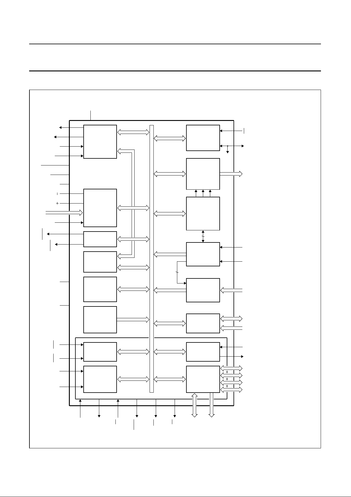
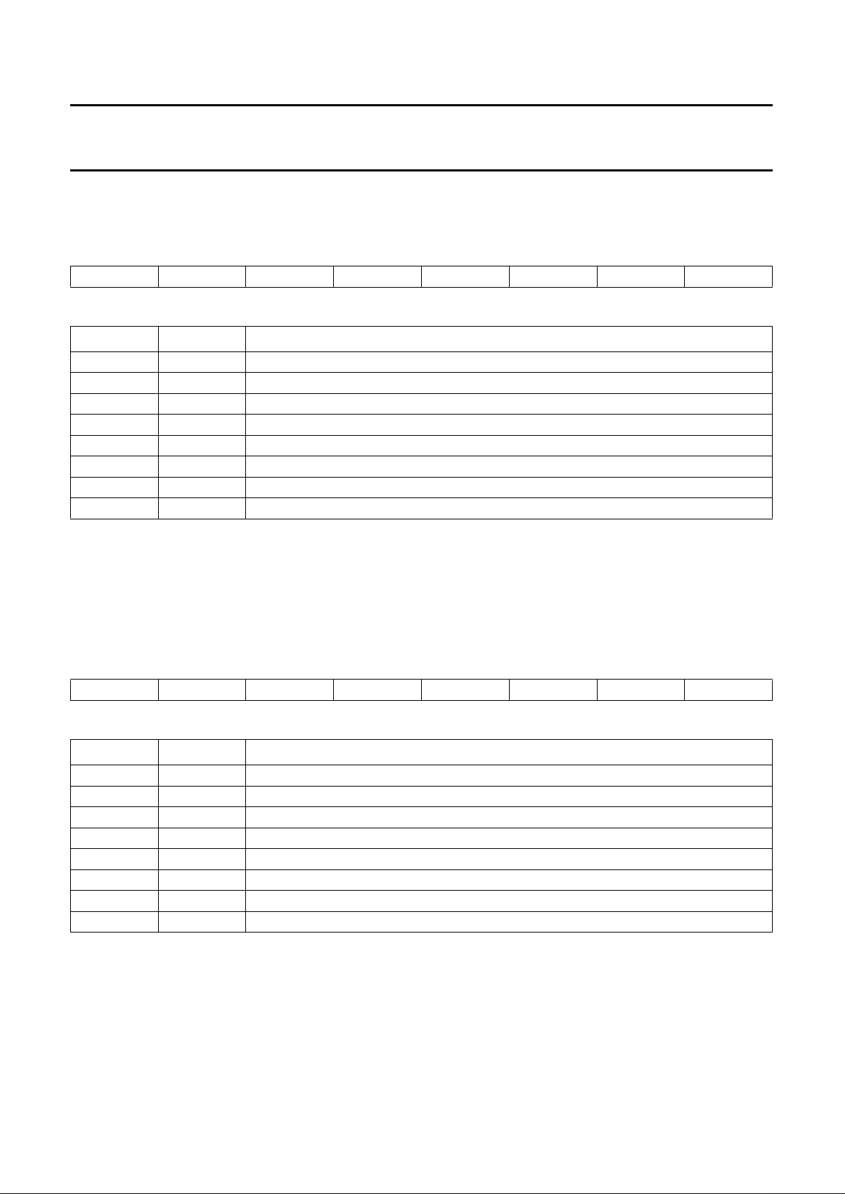
2 GENERAL DESCRIPTION
The P8xC592 is a single-chip 8-bit high-performance
microcontroller with on-chip CAN-controller, derived from
the 80C51 microcontroller family.
It uses the powerful 80C51 instruction set.
Figure 1 shows a block diagram of the P8xC592.
The P8xC592 is manufactured in an advanced CMOS
process, and is designed for use in automotive and
general industrial applications. In addition to the 80C51
standard features, the device provides a number of
dedicated hardware functions for these applications.
Two versions of the P8xC592 will be offered:
• P80C592 (without ROM)
• P83C592 (with ROM).
Hereafter these versions will be referred to as P8xC592.
The temperature range includes (max. f
CLK
= 16 MHz):
•−40 to +85 °C version, for general applications
•−40 to +125 °C version for automotive applications.
The P8xC592 combines the functions of the P8xC552
(microcontroller) and the PCA82C200 (Philips
CAN-controller) with the following enhanced features:
• 16 kbytes Program Memory
• 2 × 256 bytes Data Memory
• DMA between CAN Transmit/Receive Buffer and
internal RAM.
The main differences between P8xC592 and P8xC552
are:
• 16 kbytes programmable ROM (P8xC552 has 8 kbytes)
• Additional 256 bytes RAM
• A CAN-controller instead of the I2C-serial interface.
3 ORDERING INFORMATION
TYPE
NUMBER
PACKAGE
TEMPERATURE
RANGE (°C)
FREQ.
(MHz)
NAME DESCRIPTION VERSION
Without ROM
P80C592FFA
PLCC68 plastic leaded chip carrier; 68 leads SOT188-2
−40 to +85
1.2 to 16
P80C592FHA −40 to +125
With ROM
P83C592FFA
PLCC68 plastic leaded chip carrier; 68 leads SOT188-2
−40 to +85
1.2 to 16
P83C592FHA −40 to +125
Page 4
1996 Jun 27 4
Philips Semiconductors Product specification
8-bit microcontroller with on-chip CAN P8xC592
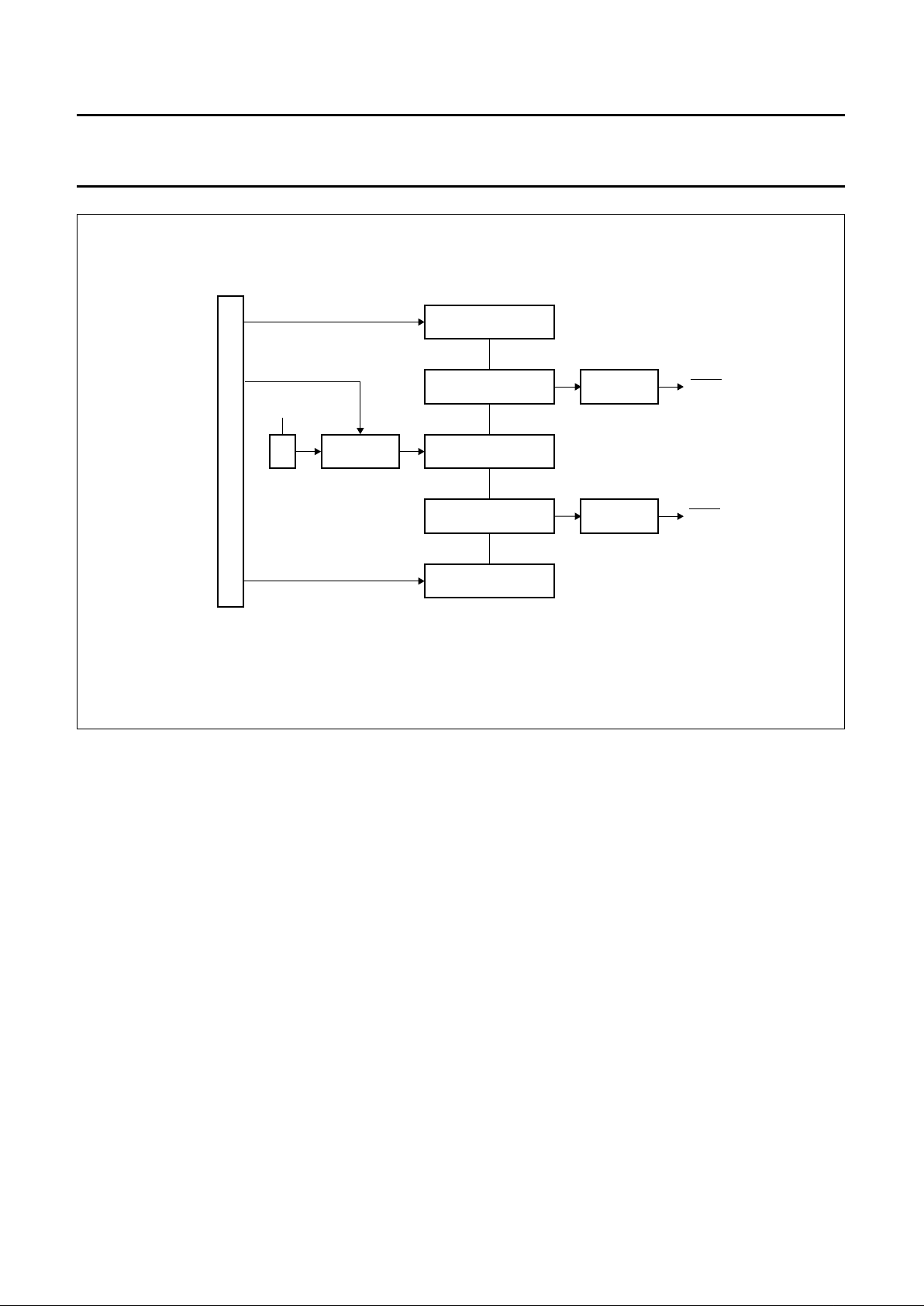
4 BLOCK DIAGRAM
handbook, full pagewidth
handbook, full pagewidth
MGA146
RD
WR
PSEN
XTAL2
XTAL1
A8 to A15
AD0 to AD7
ADC0 to ADC7
EA
CTX1
CTX0CRX0
CRX1
STADC
AV
ref
AV
SS
AV
DD
RST EWCMSR0 to CMSR5
CMT0, CMT1
RT2
T2
P4P5RXDTXDP3P2P1P0
T0
T1 INT0 INT1
V
DD
V
SS
CV
SS
THREE
16-BIT
COMPARATORS
WITH
REGISTERS
PARALLEL
I/O PORTS
&
EXT. BUS
SERIAL
UART
PORT
8-BIT
I/O
PORTS
FOUR
16-BIT
CAPTURE
LATCHES
T2
16-BIT
TIMER/
EVENT
COUNTER
16
16
COMPARATOR
OUTPUT
SELECTION
T3
WATCHDOG
TIMER
T0, T1
TWO 16 - BIT
TIMER/
EVENT
COUNTERS
80C51
core
excluding
ROM/RAM
CPU
PROGRAM
MEMORY
AUXILIARY
MEMORY
DATA
MEMORY
DUAL
PWM
CAN
ADC
DMA - BUS
INTERNAL BUS
P8xC592
REF
16K x 8
ROM
PWM0
PWM1
1/2AV
DD
256 x 8
RAM
256 x 8
RAM
CT0I/INT2 to
CT3I/INT5
(4)
(4) (4) (2) (2) (2) (5)
(6)
(7)
(4)(4)(4)(4) (2) (2)
(4)
(1)
(3)
Fig.1 Block diagram.
(1) Alternative function of Port 0.
(2) Alternative function of Port 1.
(3) Alternative function of Port 2.
(4) Alternative function of Port 3.
(5) Alternative function of Port 4.
(6) Alternative function of Port 5.
(7) Not present in P80C592.
Page 5
1996 Jun 27 5
Philips Semiconductors Product specification
8-bit microcontroller with on-chip CAN P8xC592
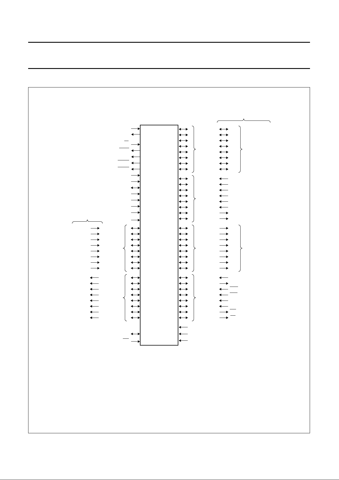
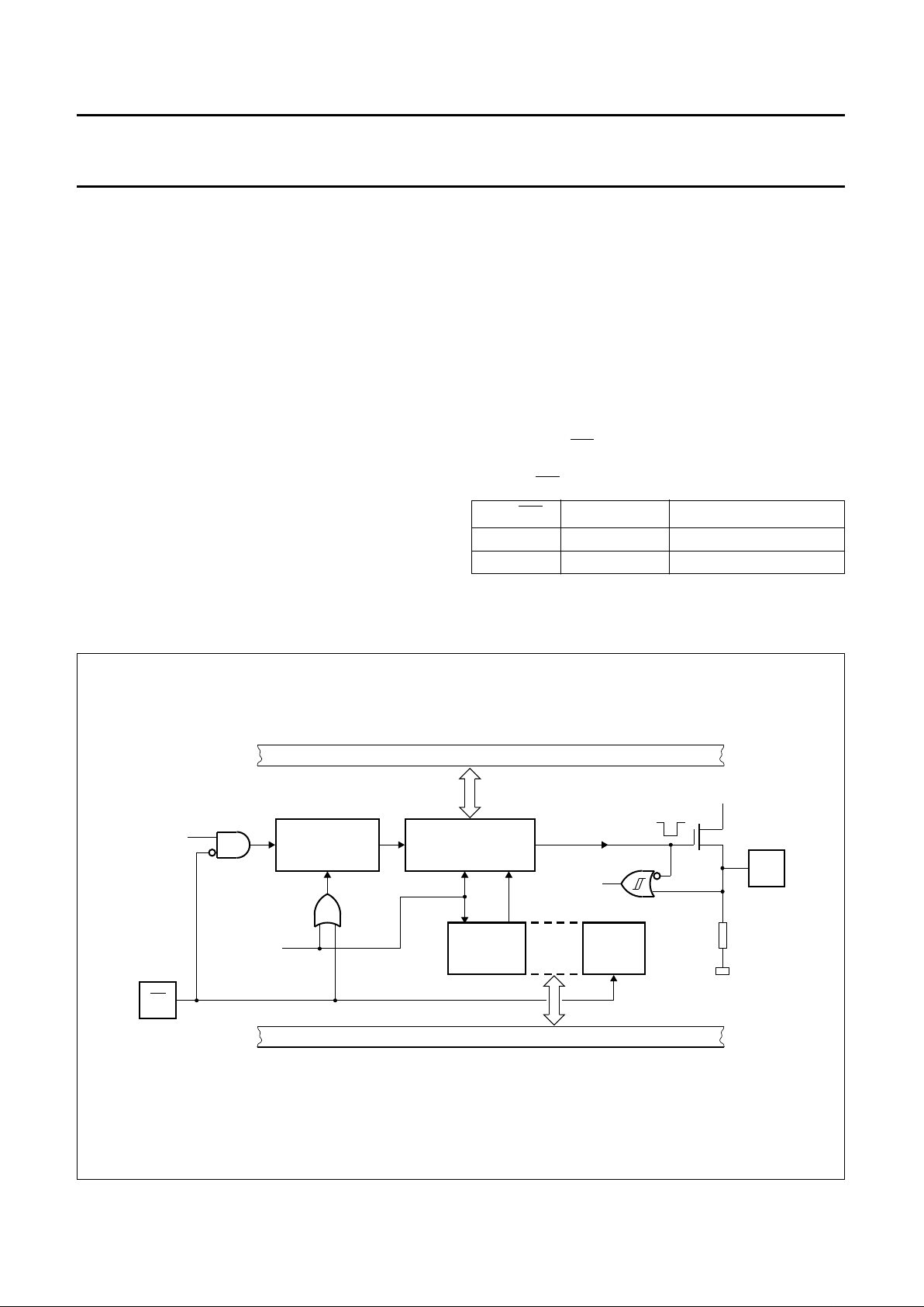
5 PINNING
Fig.2 Pin functions.
handbook, full pagewidth
MGA147 - 2
P8xC592
0
1
2
3
4
5
6
7
PORT 0
CV
SS
SS
V
DD
V
0
1
2
3
4
5
6
7
PORT 1
0
1
2
3
4
5
6
7
PORT 3
AD0
AD1
AD2
AD3
AD4
AD5
AD6
AD7
LOW ORDER
ADDRESS
AND
DATA BUS
alternative function
0
1
2
3
4
5
6
7
PORT 2
A8
A9
A10
A11
A12
A13
A14
A15
HIGH ORDER
ADDRESS
BUS
CT0I/INT2
CT1I/INT3
CT2I/INT4
CT3I/INT5
T2
RT2
CTX0
CTX1
0
1
2
3
4
5
6
7
PORT 5
0
1
2
3
4
5
6
7
PORT 4
RST
EW
alternative function
ADC0
CMSR0
ADC1
ADC2
ADC3
ADC4
ADC5
ADC6
ADC7
CMSR1
CMSR2
CMSR3
CMSR4
CMSR5
CMT0
CMT1
AV
SS
AV
ref+
AV
ref –
STADC
DD
AV
PSEN
CRX0
CRX1
PWM0
PWM1
XTAL1
XTAL2
RXD/DATA
TXD/CLOCK
T0
T1
RD
WR
INT1
INT0
ALE
EA
REF
Page 6
1996 Jun 27 6
Philips Semiconductors Product specification
8-bit microcontroller with on-chip CAN P8xC592
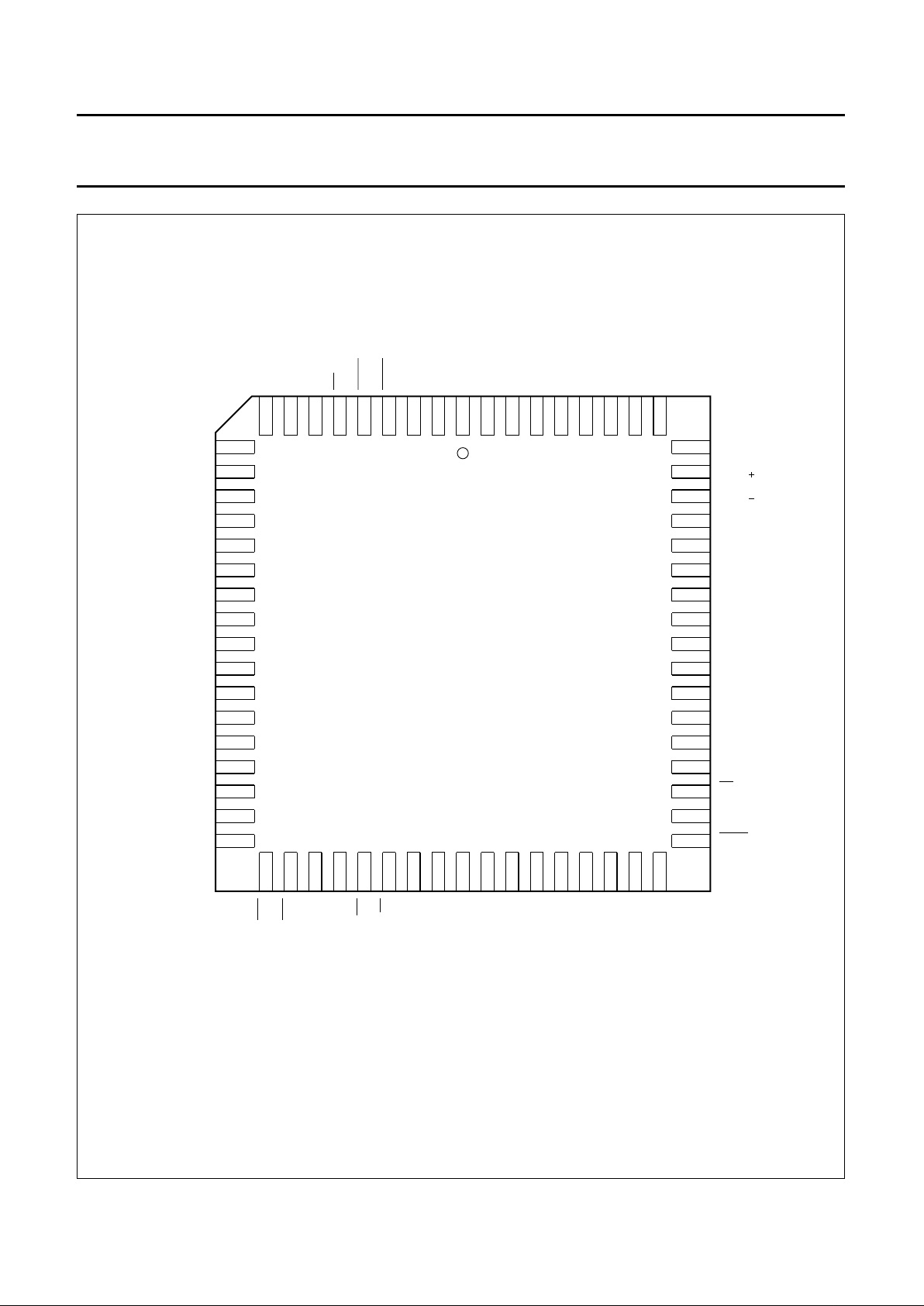
Fig.3 Pin configuration PLCC68/SOT188-2 version (P8xC592FFA; FHA;).
andbook, full pagewidth
P4.3/CMSR3
P4.4/CMSR4
P4.5/CMSR5
P4.6/CMT0
P4.7/CMT1
RST
P1.0/CT0I/INT2
P1.1/CT1I/INT3
P1.2/CT2I/INT4
P1.3/CT3I/INT5
P1.4/T2
P1.5/RT2
CV
SS
P1.6/CTX0
P1.7/CTX1
P3.0/RXD
P3.1/TXD
27
28
29
30
31
32
33
34
35
36
37
38
39
40
41
42
43
9
8
7
6
5
4
3
2
1
68
67
66
65
64
63
62
61
10
11
12
13
14
15
16
17
18
19
20
21
22
23
24
25
26
60
59
58
57
56
55
54
53
52
51
50
49
48
47
46
45
44
P4.2/CMSR2
P4.1/CMSR1
P4.0/CMSR0
EW
PWM1
PWM0
STADC
V
DD
P5.0/ADC0
P5.1/ADC1
P5.2/ADC2
P5.3/ADC3
P5.4/ADC4
P5.5/ADC5
P5.6/ADC6
P5.7/ADC7
AV
DD
P8xC592
MGA148 - 1
AV
SS
CRX0
CRX1
REF
P0.0/AD00
P0.1/AD01
P0.2/AD02
P0.3/AD03
P0.4/AD04
P0.5/AD05
P0.6/AD06
P0.7/AD07
ALE
PSEN
AV
ref
AV
ref
EA
P3.7/RD
XTAL1
P2.3/A11
P3.2/INT0
P3.3/INT1
P3.4/T0
P3.5/T1
P3.6/WR
XTAL2
P2.0/A08
P2.1/A09
P2.2/A10
P2.4/A12
P2.5/A13
P2.6/A14
P2.7/A15
V
SS
Page 7

1996 Jun 27 7
Philips Semiconductors Product specification
8-bit microcontroller with on-chip CAN P8xC592
Table 1 Pin description for single function pins (SOT188-2; see note 1)
Notes
1. To avoid a ‘latch up’ effect at power-on: VSS− 0.5 V < ‘voltage on any pin at any time’ < VDD+ 0.5 V.
2. Triggered by a rising edge. ADC operation can also be started by software.
3. RST also provides a reset pulse as output when timer T3 overflows or after a CAN wake-up from Power-down.
4. ALE is activated every six oscillator periods. During an external data memory access one ALE pulse is skipped.
5. See Section 7.1, Table 3 for EA operation. For P83Cxxx microcontrollers specified with the option ‘ROM-code
protection’, the EA pin is latched during reset and is ‘don't care’ after reset, regardless of whether the ROM-code
protection is selected or not.
SYMBOL PIN DESCRIPTION
V
DD
2 Power supply, digital part (+5 V). For normal operation and power reduced modes.
STADC 3 Start ADC operation. Input starting analog-to-digital conversion (note 2). This pin must not float.
PWM0 4 Pulse width modulation output 0.
PMW1 5 Pulse width modulation output 1.
EW 6 Enable Watchdog Timer (WDT): enable for T3 Watchdog Timer and disable Power-down mode.
This pin must not float.
RST 15 Reset: input to reset the P8xC592 (note 3).
CV
SS
22 CAN ground potential for the CAN transmitter outputs.
XTAL2 33 Crystal pin 2: output of the inverting amplifier that forms the oscillator.
When an external clock oscillator is used this pin is left open-circuit.
XTAL1 34 Crystal pin 1: input to the inverting amplifier that forms the oscillator, and input to the internal clock
generator. Receives the external clock oscillator signal, when an external oscillator is used.
V
SS
35 Ground, digital part.
PSEN 44 Program Store Enable: Read strobe to external Program Memory (active LOW).
Drive: 8 × LSTTL inputs.
ALE 45 Address Latch Enable: latches the Low-byte of the address during accesses to external memory
(note 4). Drive: 8 × LSTTL inputs; handles CMOS inputs without an external pull-up.
EA 46 External Access input. See note 5.
REF 55
1
⁄2AVDD reference voltage output respectively input (note 6).
CRX1 56 Inputs from the CAN-bus line to the differential input comparator of the on-chip CAN-controller
(note 7).
CRX0 57
AV
REF−
58 Low-end of ADC (analog-to-digital) conversion reference resistor.
AV
REF+
59 High-end of ADC (analog-to-digital) conversion reference resistor (note 8).
AV
SS
60 Ground, analog part. For ADC, CAN receiver and reference voltage.
AV
DD
61 Power supply, analog part (+5 V). For ADC, CAN receiver and reference voltage.
Page 8

1996 Jun 27 8
Philips Semiconductors Product specification
8-bit microcontroller with on-chip CAN P8xC592
6. Pin 55, REF:
a) Selection of input resp. output dependent of CAN Control Register bit 5 (CR.5; see Section 13.5.3 Table 32).
b) If the internal reference is used, then REF should be connected to AVSS via a capacitor with a value of ≥10 nF.
c) After an external reset (RST = HIGH) the internal1⁄2AVDD source is activated and, REF is a reference output.
d) If the CAN-controller is in the reset state, e.g. after an external reset, then the1⁄2AVDD source is switched off
during Power-down mode.
7. CAN-bus line:
a) CRX0 level > CRX1 level is interpreted as a logic 1 (recessive).
b) CRX0 level < CRX1 level is interpreted as a logic 0 (dominant).
8. The level of AV
REF+
must be higher than that of AV
REF−
.
Table 2 Pin description for pins with alternative functions (SOT188-2 and NO330; see note 1)
SYMBOL
PIN DESCRIPTION
DEFAULT ALTERNATIVE
Port 4
P4.0 to P4.7 7 to 14 8-bit quasi-bidirectional I/O port.
CMSR0 7 Compare and Set/Reset outputs for Timer T2.
CMSR1 8
CMSR2 9
CMSR3 10
CMSR4 11
CMSR5 12
CMT0 13 Compare and toggle outputs for Timer T2.
CMT1 14
Port 1
P1.0 to P1.7 16 to 21, 23, 24 8-bit quasi-bidirectional I/O port.
CT0I/INT2 16 Capture timer inputs for Timer T2,
or
External interrupt inputs.
CT1I/INT3 17
CT2I/INT4 18
CT3I/INT5 19
T2 20 T2 event input (rising edge triggered).
RT2 21 T2 timer reset input (rising edge triggered).
CTX0 23 CAN transmitter output 0 (note 2).
CTX1 24 CAN transmitter output 1 (note 2).
Page 9

1996 Jun 27 9
Philips Semiconductors Product specification
8-bit microcontroller with on-chip CAN P8xC592
Notes
1. To avoid a ‘latch up’ effect at power-on: VSS− 0.5 V < ‘voltage on any pin at any time’ < VDD+ 0.5 V.
2. If the CAN-controller is in the reset state (e.g. after a power-up reset; CAN Control Register bit CR.0; see
Section 13.5.3 Table 32), the CAN transmitter outputs are floating and the pins P1.6 and P1.7 can be used as
open-drain port pins. After a power-up reset the port data is HIGH, leaving the pins P1.6 and P1.7 floating.
Port 3
P3.0 to P3.7 25 to 32 8-bit quasi-bidirectional I/O port.
RXD 25 Serial Input Port.
TXD 26 Serial Output Port.
INT0 27 External interrupt inputs.
INT1 28
T0 29 Timer 0 external input.
T1 30 Timer 1 external input.
WR 31 External Data Memory Write strobe.
RD 32 External Data Memory Read strobe.
Port 2 (Sink/source: 1 × TTL = 4 × LSTTL inputs)
P2.0 to P2.7 36 to 43 8-bit quasi-bidirectional I/O port.
A08 to A15 High-order address byte for external memory.
Port 0 (Sink/source: 8 × LSTTL inputs)
P0.7 to P0.0 47 to 54 8-bit open drain bidirectional I/O port.
AD7 to AD0 Multiplexed Low-order address and
Data bus for external memory.
Port 5
P5.7 to P5.0 62 to 68, 1 8-bit input port.
ADC7 to ADC0 8 input channels to ADC.
SYMBOL
PIN DESCRIPTION
DEFAULT ALTERNATIVE
Page 10

1996 Jun 27 10
Philips Semiconductors Product specification
8-bit microcontroller with on-chip CAN P8xC592
6 FUNCTIONAL DESCRIPTION
The P8xC592 functions will be described as shown in the
following overview:
• Memory organization
• I/O Port structure
• Pulse Width Modulated outputs
• Analog-to-digital Converter
• Timers/Counters
• Serial I/O Ports
• Interrupt system
• Power reduction modes
• Oscillator circuitry
• Reset circuitry
• Instruction Set.
7 MEMORY ORGANIZATION
The Central Processing Unit (CPU) manipulates operands
in three memory spaces (see Fig.4) as follows:
• 16 kbytes internal resp. 64 kbytes external Program
Memory
• 512 bytes internal Data Memory MAIN- and AUXILIARY
RAM
• up to 64 kbytes external Data Memory
(with 256 bytes residing in the internal AUXILIARY
RAM).
handbook, full pagewidth
MGA149
INDIRECT ONLY
DIRECT AND
INDIRECT
AUXILIARY
RAM
SFRs
255
127
0
EXTERNAL
(EA = 0)
INTERNAL
(EA = 1)
MAIN RAM
INTERNAL DATA MEMORY
EXTERNAL
DATA MEMORY
PROGRAM MEMORY
EXTERNAL
64K
64K
16384
16383
0
OVERLAPPED SPACE
256
Fig.4 Memory map.
Page 11
1996 Jun 27 11
Philips Semiconductors Product specification
8-bit microcontroller with on-chip CAN P8xC592
7.1 Program Memory
The Program Memory of the P8xC592 consists of 16 kbytes ROM on-chip, externally expandible up to 64 kbytes.
Table 3 Instruction fetch controlled by
EA
Notes
1. This implementation prevents reading of the internal program code by switching from external Program Memory
during a MOVC instruction.
2. By setting a security bit the internal Program Memory content is protected, which means it cannot be read out.
If the security bit has been set to LOW there are no restrictions for the MOVC instruction.
7.2 Internal Data Memory
The internal Data Memory is physically built-up and accessible as shown in Table 4 (see Fig.5).
Table 4 Internal Data Memory size and address mode
Notes
1. MAIN RAM can be addressed directly and indirectly as in the 80C51.
2. AUXILIARY RAM (0 to 255):
a) Is indirectly addressable in the same way as the external Data Memory with MOVX instructions.
b) Access will not affect the ports P0, P2, P3.6 and P3.7 during internal program execution.
3. SFRs = Special Function Registers.
PIN EA (note 1)
INSTRUCTIONS FETCHED FROM:
ADDRESS
LOCATION
DURING RESET
LATCHED TO:
AFTER RESET
H − internal Program Memory (note 2) 0000H → 3FFFH
H − external Program Memory 4000H → FFFFH
L − 0000H → FFFFH
− ‘don’t care’ −−
INTERNAL
DATA MEMORY
SIZE LOCATION
ADDRESS MODE
POINTERS
DIRECT INDIRECT
MAIN RAM
(note 1)
256 bytes 0 to 127 X X address pointers are R0 and R1 of the
selected register bank
128 to 255 − X
AUXILIARY RAM
(note 2)
256 bytes 0 to 255 − X address pointers are R0 and R1 of the
selected register bank and the DPTR
SFRs (note 3) 128 bytes 128 to 255 X −−
Page 12
1996 Jun 27 12
Philips Semiconductors Product specification
8-bit microcontroller with on-chip CAN P8xC592
7.2.1 MAIN RAM
Four 8-bit register banks occupy the lower RAM area,
• BANK 0: location 0 to 7
• BANK 1: location 8 to 15
• BANK 2: location 16 to 23
• BANK 4: location 24 to 31.
Only one of these banks may be enabled at the same time.
The next 16 bytes, locations 32 through 45, contains
128 directly addressable bit locations.
The stack can be located anywhere in the internal MAIN
RAM address space. The stack depth is only limited by the
internal RAM space available. All registers except the
program counter and the four 8-bit register banks reside in
the SFR address space.
MGA152
7F 7E 7D 7C 7B 7A 79 78
77 76 75 74 73 72 71 70
6F 6E 6D 6C 6B 6A 69 68
67 66 65 64 63 62 61 60
5F 5E 5D 5C 5B 5A 59 58
57 56 55 54 53 52 51 50
4F 4E 4D 4C 4B 4A 49 48
47 46 45 44 43 42 41 40
3F 3E 3D 3C 3B 3A 39 38
37 36 35 34 33 32 31 30
2F 2E 2D 2C 2B 2A 29 28
27 26 25 24 23 22 21 20
1F 1E 1D 1C 1B 1A 19 18
17 16 15 14 13 12 11 10
0F 0E 0D 0C 0B 0A 09 08
07 06 05 04 03 02 01 00
18H
17H
10H
0FH
08H
07H
00H
24
23
31
16
15
8
7
0
BANK 0
BANK 1
BANK 2
BANK 3
32
33
34
35
36
37
38
39
40
41
42
43
44
45
46
47
(MSB) (LSB)
127
7FH
2FH
2EH
2DH
2CH
2BH
2AH
29H
28H
27H
26H
25H
24H
23H
22H
21H
20H
1FH
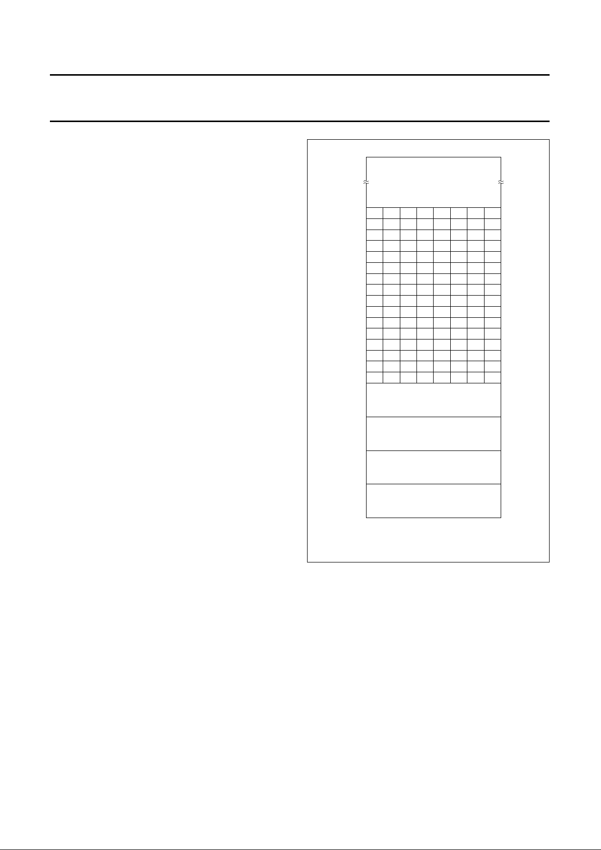
Fig.5 Internal MAIN RAM bit addresses.
7.3 External Data Memory
An access to external Data Memory locations higher than
255 will be performed with the MOVX @DPTR instructions
in the same way as in the 80C51 structure,
i.e. with P0 and P2 as data/address bus and P3.6 and P3.7
as Write and Read strobe signals.
Note that these external Data Memory locations cannot be
accessed with R0 or R1 as address pointer.
Page 13
1996 Jun 27 13
Philips Semiconductors Product specification
8-bit microcontroller with on-chip CAN P8xC592
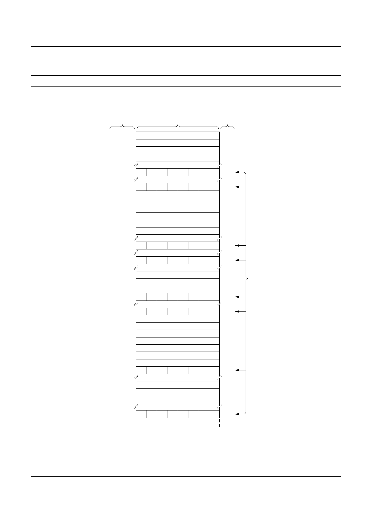
Fig.6 Special Function Register memory map (a).
handbook, full pagewidth
MGA150
FEFF FD FC FB FA F9 F8
F6F7 F5 F4 F3 F2 F1 F0
EEEF ED EC EB EA E9 E8
E6E7 E5 E4 E3 E2 E1 E0
DEDF DD DC DB DA D9 D8
D6D7 D5 D4 D3 D2 D1 D0
CECF CD CC CB CA C9 C8
C6C7 C5 C4 C3 C2 C1 C0
BIT ADDRESS
REGISTER
MNEMONIC
FFH
DIRECT
BYTE
ADDRESS (HEX)
FEH
FDH
FCH
F8H
F0H
EFH
EEH
EDH
ECH
EBH
EAH
E8H
E0H
DBH
DAH
D9H
D8H
D0H
CFH
CEH
CDH
CCH
CBH
CAH
C9H
C8H
C6H
C5H
C4H
C0H
SFRs containing
directly addressable
bits
T3
PWMP
PWM1
PWM0
IP1
B
RTE
STE
# TMH2
# TML2
CTCON
TM2CON
IEN1
ACC
CANADR
CANDAT
CANCON
CANSTA
PSW
# CTH3
# CTH2
# CTH1
# CTH0
CMH2
CMH1
CMH0
TM2IR
# ADCH
ADCON
# P5
P4
# denotes read-only registers
Page 14
1996 Jun 27 14
Philips Semiconductors Product specification
8-bit microcontroller with on-chip CAN P8xC592
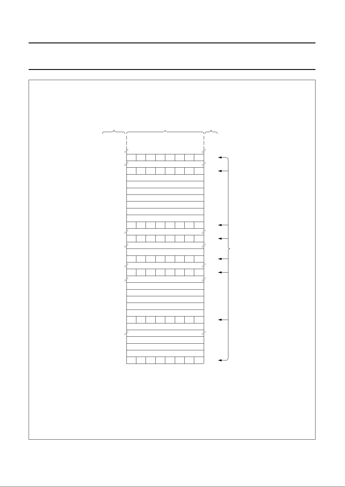
Fig.7 Special Function Register memory map (b).
handbook, full pagewidth
MGA151
BEBF BD BC BB BA B9 B8
B6B7 B5 B4 B3 B2 B1 B0
AEAF AD AC AB AA A9 A8
A6A7 A5 A4 A3 A2 A1 A0
9E9F 9D 9C 9B 9A 99 98
9697 95 94 93 92 91 90
8E8F 8D 8C 8B 8A 89 88
8687 85 84 83 82 81 80
BIT ADDRESS
REGISTER
MNEMONIC
DIRECT
BYTE
ADDRESS (HEX)
B8H
B0H
AFH
AEH
ADH
ACH
ABH
AAH
A8H
A0H
99H
98H
90H
8DH
8CH
8BH
8AH
89H
88H
87H
83H
82H
81H
80H
SFRs containing
directly addressable
bits
IP0
P3
# CTL3
P2
S0BUF
S0CON
P1
TH1
TH0
TL1
TL0
TMOD
PCON
DPH
DPL
SP
P0
# denotes read-only registers
# CTL2
# CTL1
# CTL0
CML2
CML1
CML0
IEN0
TCON
A9H
Page 15

1996 Jun 27 15
Philips Semiconductors Product specification
8-bit microcontroller with on-chip CAN P8xC592
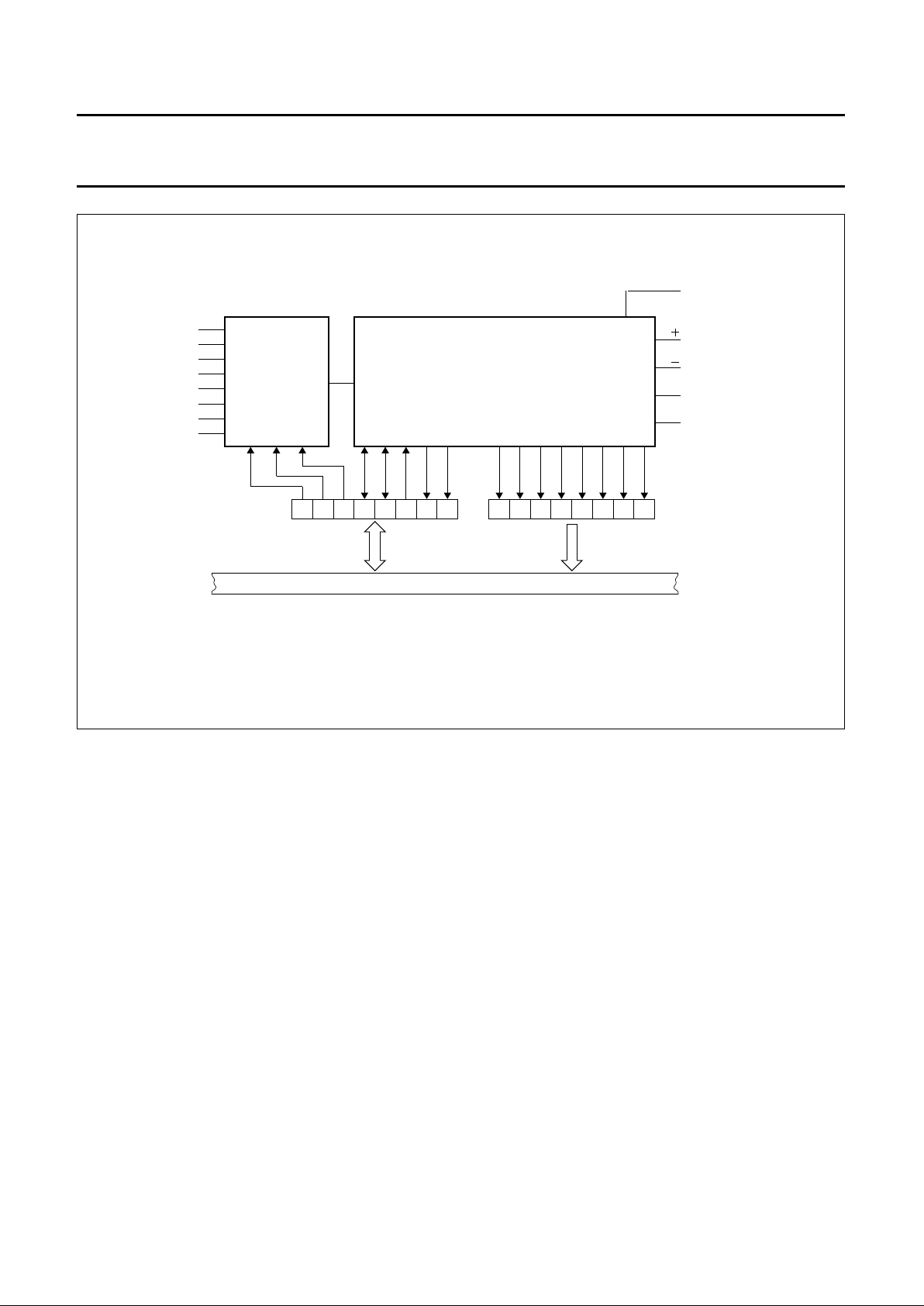
8 I/O PORT STRUCTURE
The P8xC592 has six 8-bit parallel ports: Port 0 to Port 5. In addition to the standard 8-bit parallel ports, the I/O facilities
also include a number of special I/O lines. The use of a Port 1, Port 3 or Port 4 pins as an alternative function is carried
out automatically provided the associated SFR bit is set HIGH.
Table 5 Default Port functions
Table 6 Alternative Port functions
PORT TYPE FUNCTION REMARKS
Port 0 I/O The same as in the 80C51 Except for the additional functions of P1.6 and
P1.7.
Port 1 I/O
Port 2 I/O
Port 3 I/O
Port 4 I/O Parallel l/O port Parallel I/O function is identical to Port1, 2 and 3.
Port 5 I Parallel input port with an input function only May be used as normal inputs if the ADC function
is inoperative.
PORT TYPE FUNCTION REMARKS
Port 0 I/O Multiplexed Low-order address and
Data bus for external memory (AD7 to AD0)
Provides the multiplexed Low-order address and
data bus used for expanding the P8xC592 with
standard memories and peripherals.
Port 1 I/O Capture timer inputs for Timer T2
(CT0I to CT3I), or
External interrupt request inputs
(INT2 to INT5)
External interrupt request inputs, if capture
information is not utilized.
T2 event input (T2) External counter input.
T2 timer reset input (RT2) External counter reset input.
CAN transmitter output 0 (CTX0) CTX0 and CTX1 outputs of the CAN interface
(note 1).
CAN transmitter output 1 (CTX1)
Port 2 I/O High-order address byte for external memory
(A08 to A15)
Port 2 provides the High-order address bus when
the P8xC592 is expanded with external Program
Memory and/or external Data Memory.
Port 3 I/O Serial Input Port (RXD) Receiver input of serial port SIO0 (UART).
Serial Output Port (TXD) Transmitter output of serial port SIO0 (UART).
External interrupt (
INT0) External interrupt request inputs.
External interrupt (
INT1)
Timer 0 external input (T0) Counter inputs.
Timer 1 external input (T1)
External data memory Write strobe (
WR) Control signal to write to external Data Memory.
External data memory Read strobe (
RD) Control signal to read from external Data Memory.
Port 4 I/O Compare and Set/Reset outputs
(CMSR0 to CMSR5)
Can be configured to provide signals indicating a
match between Timer counter T2 and its compare
registers.
Compare and toggle outputs (CMT0, CMT1)
Port 5 I Input channels to ADC (ADC7 to ADC0) Port 5 may be used in conjunction with the ADC
interface (note 2).
Page 16
1996 Jun 27 16
Philips Semiconductors Product specification
8-bit microcontroller with on-chip CAN P8xC592
Notes to the alternative Port functions
1. Port lines P1.6 and P1.7 may be selected as CTX0 and CTX1 outputs of the serial port SIO1 (CAN).
After reset P1.6 and P1.7 may be used as normal I/O ports, if the CAN interface is not used.
2. Unused analog inputs can be used as digital inputs. As Port 5 lines may be used as inputs to the ADC, these digital
inputs have an inherent hysteresis to prevent the input logic from drawing too much current from the power lines
when driven by analog signals.
Channel-to-channel crosstalk should be taken into consideration when both digital and analog signals are
simultaneously input to Port 5 (see Chapter 20).
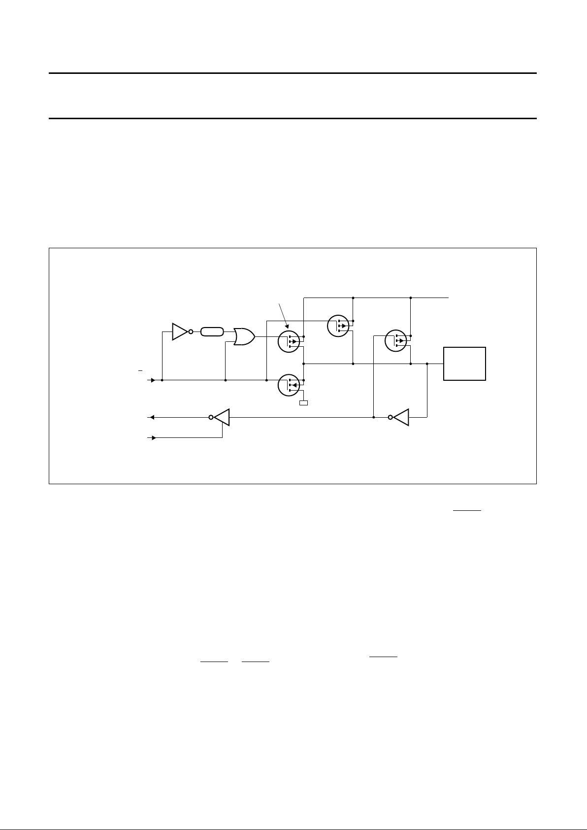
Fig.8 I/O buffers in the P8xC592 (P1.0 to P1.5, Ports 2, 3, and 4).
handbook, full pagewidth
MGA153
p1
p2
p3
input data
read port pin
2 oscillator
periods
n
strong pull-up
I/O PIN
PORT
1, 2, 3 or 4
+5 V
I1
Q
from port latch
INPUT
BUFFER
9 PULSE WIDTH MODULATED OUTPUTS (PWM)
Two Pulse Width Modulated (PWM) output channels are
available with the P8xC592. These channels provide
output pulses of programmable length and interval.
The repetition frequency is defined by an 8-bit prescaler
PWMP which generates the clock for the counter.
Both the prescaler and counter are common to both PWM
channels. The 8-bit counter counts modulo 255 i.e. from
0 to 254 inclusive. The value of the 8-bit counter is
compared to the contents of two registers:
PWM0 and PWM1.
Provided the contents of either of these registers is greater
than the counter value, the output of PWM0 or PWM1 is
set LOW. If the contents of these register are equal to, or
less than the counter value, the output will be HIGH. The
pulse-width-ratio is therefore defined by the contents of the
register PWM0 and PWM1. The pulse-width-ratio is in the
range of 0 to
255
⁄
255
and may be programmed in
increments of1⁄
255
.
The repetition frequency f
PWM
, at the PWMn outputs is
given by:
When using an oscillator frequency of 16 MHz, for
example, the above formula would give a repetition
frequency range of 123 Hz to 31.4 kHz.
By loading the PWM registers with either 00H or FFH, the
PWM outputs can be retained at a constant HIGH or LOW
level respectively. When loading FFH to the PWM
registers, the 8-bit counter will never actually reach this
(FFH) value.
Both output pins
PWMn are driven by push-pull drivers,
and are not shared with any other function.
f
PWM
f
CLK
2 PWMP 1+()× 255×
--------------------------------------------------------------
=
Page 17

1996 Jun 27 17
Philips Semiconductors Product specification
8-bit microcontroller with on-chip CAN P8xC592
9.1 Prescaler frequency control register (PWMP)
Table 7 Prescaler frequency control register (address FEH)
Table 8 Description of PWMP bits
9.2 Pulse Width Register 0 (PWM0)
Table 9 Pulse Width Register (address FCH)
Table 10 Description of PWM0 bits
9.3 Pulse Width Register 1 (PWM1)
Table 11 Pulse width register (address FDH)
Table 12 Description of PWM1 bits
76543210
PWMP.7 PWMP.6 PWMP.5 PWMP.4 PWMP.3 PWMP.2 PWMP.1 PWMP.0
BIT SYMBOL FUNCTION
7
to
0
PWMP.7
to
PWMP.0
Prescaler division factor.
The Prescaler division factor = (PWMP) + 1.
76543210
PWM0.7 PWM0.6 PWM0.5 PWM0.4 PWM0.3 PWM0.2 PWM0.1 PWM0.0
BIT SYMBOL FUNCTION
7
to
0
PWM0.7
to
PWM0.0
Pulse width ratio.
76543210
PWM1.7 PWM1.6 PWM1.5 PWM1.4 PWM1.3 PWM1.2 PWM1.1 PWM1.0
BIT SYMBOL FUNCTION
7
to
0
PWM1.7
to
PWM1.0
Pulse width ratio.
LOW/HIGH ratio of PWMn signals
PWMn()
255 PWMn()–
----------------------------------------- -
=
LOW/HIGH ratio of PWMn signals
PWMn()
255 PWMn()–
----------------------------------------- -
=
Page 18
1996 Jun 27 18
Philips Semiconductors Product specification
8-bit microcontroller with on-chip CAN P8xC592
Fig.9 Functional diagram of Pulse Width Modulated outputs.
handbook, full pagewidth
MGA154
I
N
T
E
R
N
A
L
B
U
S
f
clk
PWMP
PWM1
PRESCALER
8-BIT COUNTER1/2
PWM0
8-BIT COMPARATOR
8-BIT COMPARATOR
OUTPUT
BUFFER
PWM1
OUTPUT
BUFFER
PWM0
10 ANALOG-TO-DIGITAL CONVERTER (ADC)
The analog input circuitry consists of an 8-input analog
multiplexer and an ADC with 10-bit resolution. The analog
reference voltage and analog power supplies are
connected via separate input pins. The conversion takes
50 machine cycles i.e. 37.5 µs at 16 MHz oscillator
frequency. The input voltage swing is from 0 V to AVDD.
The ADC is controlled using the ADCON control register.
Register bits ADCON.0 to ADCON.2 select the input
channels of the analog multiplexer (see Fig.10).
The completion of the 10-bit analog-to-digital conversion is
flagged by ADCI in the ADCON register and the result is
stored in the SFR ADCH (upper 8-bits) and the 2 lower bits
(ADC.1 and ADC.0) in register ADCON.
An analog-to-digital conversion in progress is unaffected
by an external or software ADC start. The result of a
completed conversion remains unchanged provided
ADCI = HIGH. While ADCI or ADCS are HIGH, a new ADC
START will be blocked and consequently lost. An
analog-to-digital conversion already in progress is aborted
when the Idle or Power-down mode is entered.
The result of a completed conversion (ADCI = HIGH)
remains unaffected during the Idle mode.
The LOW-to-HIGH transition of STADC is recognized at
the end of a machine cycle and the conversion
commences at the beginning of the next cycle. When a
conversion is initiated by software, the conversion starts at
the beginning of the machine cycle following the
instruction that sets ADCS.
The next two machine cycles are used to initiate the
converter. At the end of this first cycle, the ADCS status
flag is set to HIGH while the conversion is in progress.
Sampling of the analog input commences at the end of the
second cycle.
During the next eight machine cycles, the voltage at the
previously selected pin of Port 5 is sampled and this input
voltage should be stable in order to obtain a useful sample.
In any case, the input voltage slew rate must be less than
10 V/ms (5 V conversion range) in order to prevent an
undefined result. The conversion takes four machine
cycles per bit.
Page 19

1996 Jun 27 19
Philips Semiconductors Product specification
8-bit microcontroller with on-chip CAN P8xC592
10.1 ADC Control register (ADCON)
Table 13 ADC Control register (address C5H)
Table 14 Description of the ADCON bits
Table 15 ADCI and ADCS operating modes
If ADCI is cleared by software while ADCS is set at the same time a new analog-to-digital conversion with the same
channel-number may be started. It is recommended to reset ADCI before ADCS is set.
Note
1. Start of a new conversion requires ADCI = 0.
76543210
ADC.1 ADC.0 ADEX ADCI ADCS AADR2 AADR1 AADR0
BIT SYMBOL FUNCTION
7 ADC.1 Bit 1 of ADC converted value.
6 ADC.0 Bit 0 of ADC converted value.
5 ADEX Enable external start of conversion by STADC. If ADEX is:
LOW, then conversion cannot be started externally by STADC (only by software by setting ADCS)
HIGH, then conversion can be started externally by a rising edge on STADC or externally.
4 ADCI ADC interrupt flag. This flag is set when an analog-to-digital conversion result is ready to be read.
If enabled, an interrupt is invoked. The flag must be cleared by software.
It cannot be set by software (see Table 15).
3 ADCS ADC start and status. Setting this bit starts an analog-to-digital conversion. It may be set by
software or by the external signal STADC. The ADC logic ensures that this signal is HIGH while the
ADC is busy. On completion of the conversion, ADCS is reset at the same time the interrupt flag
ADCI is set. ADCS can not be reset by software (see Table 15).
2 AADR2 Analog input select. This binary coded address selects one of the eight analog port pins of P5 to be
input to the converter. It can only be changed when ADCI and ADCS are both LOW. AADR2 is the
MSB. (e.g. 100B selects the analog input channel ADC4)
1 AADR1
0 AADR0
ADCI ADCS OPERATION
0 0 ADC not busy, a conversion can be started.
0 1 ADC busy, start of a new conversion is blocked.
1 X (don’t care) Conversion completed; see note 1.
Page 20
1996 Jun 27 20
Philips Semiconductors Product specification
8-bit microcontroller with on-chip CAN P8xC592
andbook, full pagewidth
MGA155
ADC0
ANALOG INPUT
MULTIPLEXER
10-BIT A/D
CONVERTER
ADCON
1234567012345670
STADC
analog reference
supply (analog part)
ground (analog part)
ADCH
INTERNAL BUS
ADC1
ADC2
ADC3
ADC4
ADC5
ADC6
ADC7
Fig.10 Functional diagram of analog input.
Page 21

1996 Jun 27 21
Philips Semiconductors Product specification
8-bit microcontroller with on-chip CAN P8xC592
11 TIMERS/COUNTERS
The P8xC592 contains:
• Three 16-bit timer/event counters:
Timer 0, Timer 1 and Timer T2
• One 8-bit timer, T3 (Watchdog WDT).
11.1 Timer 0 and Timer 1
Timer 0 and Timer 1 may be programmed to carry out the
following functions:
• Measure time intervals and pulse durations
• Count events
• Generate interrupt requests.
Timer 0 and Timer 1 can be programmed independently to
operate in 3 modes:
Mode 0 8-bit timer or 8-bit counter each with divide-by-32
prescaler.
Mode 1 16-bit timer-interval or event counter.
Mode 2 8-bit timer-interval or event counter with
automatic reload upon overflow.
Timer 0 can be programmed to operate in an additional
mode as follows:
Mode 3 one 8-bit time-interval or event counter and one
8-bit timer-interval counter.
When Timer 0 is in Mode 3, Timer 1 can be programmed
to operate in Modes 0, 1 or 2 but cannot set an interrupt
flag or generate an interrupt. However, the overflow from
Timer 1 can be used to pulse the Serial Port baud-rate
generator.
The frequency handling range of these counters with a
16 MHz crystal is as follows:
• In the timer function, the timer is incremented at a
frequency of 1.33 MHz (
1
⁄12 of the oscillator frequency)
• 0 Hz to an upper limit of 0.66 MHz (1⁄24 of the oscillator
frequency) when programmed for external inputs.
Both internal and external inputs can be gated to the
counter by a second external source for directly measuring
pulse durations. When configured as a counter, the
register is incremented on every falling edge on the
corresponding input pin, T0 or T1.
The earliest moment, when the incremented register value
can be read is during the second machine cycle following
the machine cycle within which the incrementing pulse
occurred.The counters are started and stopped under
software control. Each one sets its interrupt request flag
when it overflows from all HIGHs to all LOWs
(or automatic reload value), with the exception of Mode 3
as previously described.
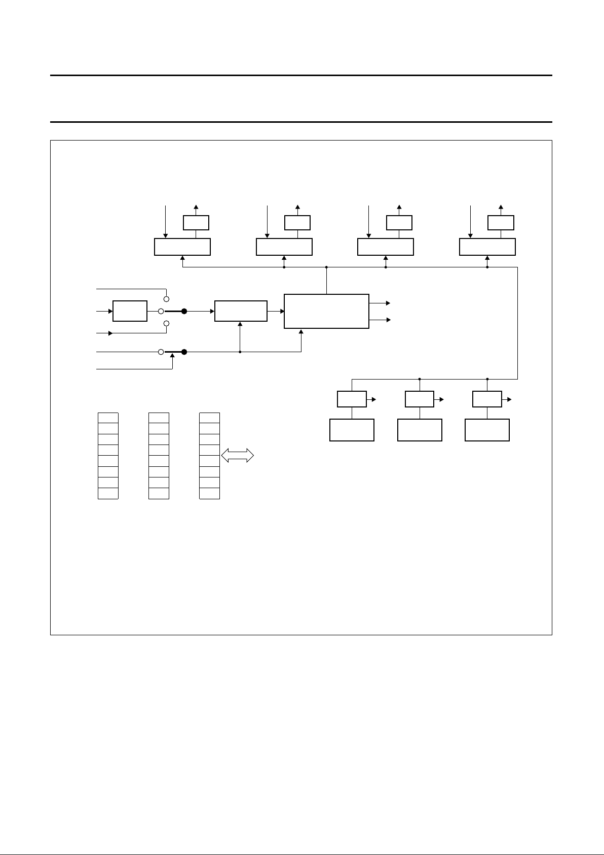
11.2 Timer T2 Capture and Compare Logic
Timer T2 is a 16-bit timer/counter which has capture and
compare facilities (see Fig.11).
The 16-bit timer/counter is clocked via a prescaler with a
programmable division factor of 1, 2, 4 or 8. The input of
the prescaler is clocked with
1
⁄12 of the oscillator
frequency, or by an external source connected to the T2
input, or it is switched off. The maximum repetition rate of
the external clock source is1⁄12f
CLK
, twice that of Timer 0
and Timer 1. The prescaler is incremented on a rising
edge. It is cleared if its division factor or its input source is
changed, or if the timer/counter is reset.
T2 is readable ‘on the fly’, without any extra read latches;
this means that software precautions have to be taken
against misinterpretation at overflow from least to most
significant byte while T2 is being read. T2 is not loadable
and is reset by the RST signal or at the positive edge of the
input signal RT2, if enabled. In the Idle mode the
timer/counter and prescaler are reset and halted.
T2 is connected to four 16-bit Capture Registers: CT0,
CT1, CT2 and CT3. A rising or falling edge on the inputs
CT0I, CT1I, CT2I or CT3I (alternative function of Port 1)
results in loading the contents of T2 into the respective
Capture Registers and an interrupt request.
Using the Capture Register CTCON, these inputs may
invoke capture and interrupt request on a positive edge, a
negative edge or on both edges. If neither a positive nor a
negative edge is selected for capture input, no capture or
interrupt request can be generated by this input.
The contents of the Compare Registers CM0, CM1 and
CM2 are continually compared with the counter value of
Timer T2. When a match occurs, an interrupt may be
invoked. A match of CM0 sets the bits 0 to 5 of Port 4, a
CM1 match resets these bits and a CM2 match toggles bits
6 and 7 of Port 4, provided these functions are enabled by
the STE/RTE registers. A match of CM0 and CM1 at the
same time results in resetting bits 0 to 5 of Port 4. CM0,
CM1 and CM2 are reset by the RST signal.
Port 4 can be read and written by software without
affecting the toggle, set and reset signals. At a byte
overflow of the least significant byte, or at a 16-bit overflow
of the timer/counter, an interrupt sharing the same
interrupt vector is requested. Either one or both of these
overflows can be programmed to request an interrupt.
All interrupt flags must be reset by software.
Page 22
1996 Jun 27 22
Philips Semiconductors Product specification
8-bit microcontroller with on-chip CAN P8xC592
handbook, full pagewidth
MGA156
STE
R
RTE
I/O port 4
= set
= reset
= toggle
= toggle status
S
R
T
TG
T2 SFR address: TML2 = lower 8 bits
TMH2 = higher 8 bits
INT
COMP
CM0 (S)
INT
COMP
CM1 (R)
INT
COMP
CM2 (T)
CT3I INT
CTI3
CT3
off
f
CLK
T2
RT2
T2ER
external reset
enable
PRESCALER
1/12
T2 COUNTER
8-bit overflow interrupt
16-bit overflow interrupt
CT2I INT
CTI2
CT2
CT1I INT
CTI1
CT1
CT0I INT
CTI0
CT0
R
R
R
R
R
T
T
P4.0
P4.1
P4.2
P4.3
P4.4
P4.5
P4.6
P4.7
S
S
S
S
S
S
TG
TG
Fig.11 Block diagram of Timer T2 configuration.
Page 23
1996 Jun 27 23
Philips Semiconductors Product specification
8-bit microcontroller with on-chip CAN P8xC592
11.2.1 COUNTER CONTROL REGISTER (TM2CON)
Table 16 Counter Control register (address EAH)
Table 17 Description of the TM2CON bits
76543210
T2IS1 T2IS0 T2ER T2B0 T2P1 T2P0 T2MS1 T2MS0
BIT SYMBOL FUNCTION
7 T2IS1 Timer 2 16-bit overflow interrupt select.
6 T2IS0 Timer 2 byte overflow interrupt select.
5 T2ER Timer 2 external reset enable.
4 T2B0 Timer 2 byte overflow interrupt flag.
3 T2P1 Timer 2 prescaler select (see Table 18).
2 T2P0
1 T2MS1 Timer 2 mode select (see Table 19).
0 T2MS0
Table 18 Timer 2 prescaler select
T2P1 T2P0 T2 CLOCK
0 0 Clock source
01
1
⁄
2
Clock source
10
1
⁄
4
Clock source
11
1
⁄
8
Clock source
Table 19 Timer 2 mode select
T2MS1 T2MS0 MODE
0 0 Timer T2 is halted
0 1 T2 clock source =
1
⁄12f
CLK
.
1 0 Test mode; do not use
1 1 T2 clock source = pin T2
11.2.2 CAPTURE CONTROL REGISTER (CTCON)
Table 20 Capture Control register (address EBH)
Table 21 Description of the CTCON bits
76543210
CTN3 CTP3 CTN2 CTP2 CTN1 CTP1 CTN0 CTP0
BIT SYMBOL
FUNCTION
CAPTURE INTERRUPT ON
7 CTN3 CT3I negative edge
6 CTP3 CT3I positive edge
5 CTN2 CT2I negative edge
4 CTP2 CT2I positive edge
3 CTN1 CT1I negative edge
2 CTP1 CT1I positive edge
1 CTN0 CT0I negative edge
0 CTP0 CT0I positive edge
Page 24
1996 Jun 27 24
Philips Semiconductors Product specification
8-bit microcontroller with on-chip CAN P8xC592
11.2.3 TIMER INTERRUPT FLAG REGISTER (TM2IR)
Table 22 Timer Interrupt Flag register (address C8H)
Table 23 Description of the TM2IR bits (see notes 1 and 2)
Notes
1. Interrupt Enable IEN1 is used to enable/disable Timer 2 interrupts (see Section 14.1.2).
2. Interrupt Priority Register IP1 is used to determine the Timer 2 interrupt priority (see Section 14.1.4).
11.2.4 S
ET ENABLE REGISTER (STE)
Table 24 Set Enable register (address EEH)
Table 25 Description of the STE bits (see notes 1 and 2)
Notes
1. If STE.n is LOW then P4.n is not affected by a match of CM0 and T2 (n = 0, 1, 2, 3, 4, 5).
2. STE.6 and STE.7 are read only.
76543210
T2OV CMI2 CMI1 CMI0 CTI3 CTI2 CTI1 CTI0
BIT SYMBOL FUNCTION
7 T2OV T2: 16-bit overflow interrupt flag
6 CMI2 CM2: interrupt flag
5 CMI1 CM1: interrupt flag
4 CMI0 CM0: interrupt flag
3 CTI3 CT3: interrupt flag
2 CTI2 CT2: interrupt flag
1 CTI1 CT1: interrupt flag
0 CTI0 CT0: interrupt flag
76543210
TG47 TG46 SP45 SP44 SP43 SP42 SP41 SP40
BIT SYMBOL FUNCTION
7 TG47 if HIGH then P4.7 is reset on the next toggle, if LOW P4.7 is set on the next toggle
6 TG46 if HIGH then P4.6 is reset on the next toggle, if LOW P4.6 is set on the next toggle
5 SP45 if HIGH then P4.5 is set on a match of CM0 and T2
4 SP44 if HIGH then P4.4 is set on a match of CM0 and T2
3 SP43 if HIGH then P4.3 is set on a match of CM0 and T2
2 SP42 if HIGH then P4.2 is set on a match of CM0 and T2
1 SP41 if HIGH then P4.1 is set on a match of CM0 and T2
0 SP40 if HIGH then P4.0 is set on a match of CM0 and T2
Page 25

1996 Jun 27 25
Philips Semiconductors Product specification
8-bit microcontroller with on-chip CAN P8xC592
11.2.5 RESET/TOGGLE ENABLE REGISTER (RTE)
Table 26 Reset/Toggle Enable register (address EFH)
Table 27 Description of the RTE bits (note 1)
Note
1. If RTE.n is LOW then P4.n is not affected by a match of CM1 and T2 or CM2 and T2.
For more information, refer to the 8051-based
“8-bit Microcontrollers Data Handbook IC20”
.
76543210
TP47 TP46 RP45 RP44 RP43 RP42 RP41 RP40
BIT SYMBOL FUNCTION
7 TP47 if HIGH then P4.7 toggles on a match of CM2 and T2
6 TP46 if HIGH then P4.6 toggles on a match of CM2 and T2
5 RP45 if HIGH then P4.5 is reset on a match of CM1 and T2
4 RP44 if HIGH then P4.4 is reset on a match of CM1 and T2
3 RP43 if HIGH then P4.3 is reset on a match of CM1 and T2
2 RP42 if HIGH then P4.2 is reset on a match of CM1 and T2
1 RP41 if HIGH then P4.1 is reset on a match of CM1 and T2
0 RP40 if HIGH then P4.0 is reset on a match of CM1 and T2
Page 26
1996 Jun 27 26
Philips Semiconductors Product specification
8-bit microcontroller with on-chip CAN P8xC592
11.3 Watchdog Timer (T3)
In addition to Timer T2 and the standard timers (Timer 0
and Timer 1), a Watchdog Timer (WDT) comprising an
11-bit prescaler and an 8-bit timer (T3) is also provided
(see Fig.12).
The timer T3 is incremented every 1.5 ms, derived from
the oscillator frequency of 16 MHz by the following
formula:
When a timer T3 overflow occurs, the microcontroller is
reset and a reset-output-pulse is generated at pin RST.
This short output pulse (3 machine cycles) may be
suppressed if the RST pin is connected to a capacitor.
To prevent a system reset (by an overflow of the WDT), the
user program has to reload T3 within periods that are
shorter than the programmed Watchdog time interval.
If the processor suffers a hardware/software malfunction,
the software will fail to reload the timer. This failure will
produce a reset upon overflow thus preventing the
processor running out of control.
f
timer
f
CLK
12 2048×
------------------------- -
=
The Watchdog Timer can only be reloaded if the condition
flag WLE = PCON.4 has been previously set by software.
At the moment the counter is loaded the condition flag is
automatically cleared.
The timer interval between the timer's reloading and the
occurrence of a reset depends on the reloaded value. For
example, this may range from 1.5 ms to 0.375 s when
using an oscillator frequency of 16 MHz.
In the Idle state the Watchdog Timer and reset circuitry
remain active.
The Watchdog Timer (WDT) is controlled by the Enable
Watchdog pin (
EW) (see Table 28).
Table 28
EW controlling WDT and Power-down mode
PIN EW WDT POWER-DOWN MODE
LOW enabled disabled
HIGH disabled enabled
Fig.12 Functional diagram of T3 Watchdog Timer.
andbook, full pagewidth
MGA157
INTERNAL BUS
1/12 f
CLK
write
T3
PRESCALER
11-BIT
TIMER T3 (8-BIT)
LOADCLEAR
overflow
internal
reset
LOADEN
EW
LOADEN
PCON.4
PCON.1
CLEAR
WLE PD
R
RST
RST
P
V
DD
INTERNAL BUS
Page 27

1996 Jun 27 27
Philips Semiconductors Product specification
8-bit microcontroller with on-chip CAN P8xC592
12 SERIAL I/O PORT: SIO0 (UART)
The Serial Port SIO0 is a full duplex (UART) serial I/O port
i.e. it can transmit and receive simultaneously. This Serial
Port is also receive-buffered. It can commence reception
of a second byte before the previously received byte has
been read from the receive register. However, if the first
byte has still not been read by the time reception of the
second byte is complete, one of these (first or second)
bytes will be lost. The SIO0 receive and transmit registers
are both accessed via the S0BUF SFR. Writing to S0BUF
loads the transmit register, and reading S0BUF accesses
to a physically separate receive register. SIO0 can operate
in 4 modes:
Mode 0 Serial data is transmitted and received through
RXD. TXD outputs the shift clock. 8 data bits are
transmitted/received (LSB first). The baud rate is
fixed at1⁄12 of the oscillator frequency.
Mode 1 10 bits are transmitted via TXD or received
through RXD: a start bit (0), 8 data bits (LSB first),
and a stop bit (1). On receive, the stop bit is put
into RB8 of the S0CON SFR. The baud rate is
variable.
Mode 2 11 bits are transmitted through TXD or received
through RXD: a start bit (0), 8 data bits (LSB first),
a programmable 9th data bit, and a stop bit (1).
On transmit, the 9th data bit (TB8 in S0CON) can
be assigned the value of 0 or 1. With nominal
software, TB8 can be the parity bit (P in PSW).
During a receive, the 9th data bit is stored in RB8
(S0CON), and the stop bit is ignored. The baud
rate is programmable to either1⁄32 or1⁄64 of the
oscillator frequency.
Mode 3 11 bits are transmitted through TXD or received
through RXD: a start bit (0), 8 data bits (LSB first),
a programmable 9th data bit, and a stop bit (1).
Mode 3 is the same as Mode 2 except for the
baud rate which is variable in Mode 3.
In all four modes, transmission is initiated by any
instruction that writes to the S0BUF SFR.
Reception is initiated in Mode 0 when RI = 0 and REN = 1.
In the other three modes, reception is initiated by the
incoming start bit provided that REN = 1.
Modes 2 and 3 are provided for multiprocessor
communications. In these modes, 9 data bits are received
with the 9th bit written to RB8 (S0CON). The 9th bit is
followed by the stop bit. The port can be programmed so
that with receiving the stop bit, the Serial Port interrupt will
be activated if, and only if RB8 = 1.
This feature is enabled by setting bit SM2 in S0CON. This
feature may be used in multiprocessor systems.
For more information about how to use the UART in
combination with the registers S0CON, PCON, IE, SBUF
and the Timer register, refer to the 8051-based
“8-bit Microcontrollers Data Handbook IC20”
.
13 SERIAL I/O PORT: SIO1 (CAN)
SIO1 (CAN) provides the CAN (Controller Area Network)
serial-bus data communication interface. SIO1 (CAN)
replaces the SIO1 (I
2
C) serial interface as provided in the
microcontroller derivative P8xC552.
13.1 On-chip CAN-controller
CAN is the definition of a high performance
communication protocol for serial data communication.
The P8xC592 on-chip CAN-controller is a full
implementation of the CAN 2.0A protocol. With the
P8xC592 powerful local networks can be built, both for
automotive and general industrial environments. This
results in a much reduced wiring harness and enhanced
diagnostic and supervisory capabilities.
13.2 CAN Features
• Multi-master architecture
• Bus access priority determined by the message
identifier
• 2032 message identifier (2
11
standard frame CAN 2.0A)
• Guaranteed latency time for high priority messages
• Powerful error handling capability
• Data length from 0 up to 8 bytes
• Multicast and broadcast message facility
• Non destructive bit-wise arbitration
• Non-return-to-zero (NRZ) coding/decoding with
bit-stuffing
• Programmable transfer rate (up to 1 Mbit/s)
• Programmable output driver configuration
• Suitable for use in a wide range of networks including
the SAE's network classes A, B and C
• DMA providing high-speed on-chip data exchange
• Bus failure management facility
•1⁄2AVDD reference voltage.
Page 28
1996 Jun 27 28
Philips Semiconductors Product specification
8-bit microcontroller with on-chip CAN P8xC592
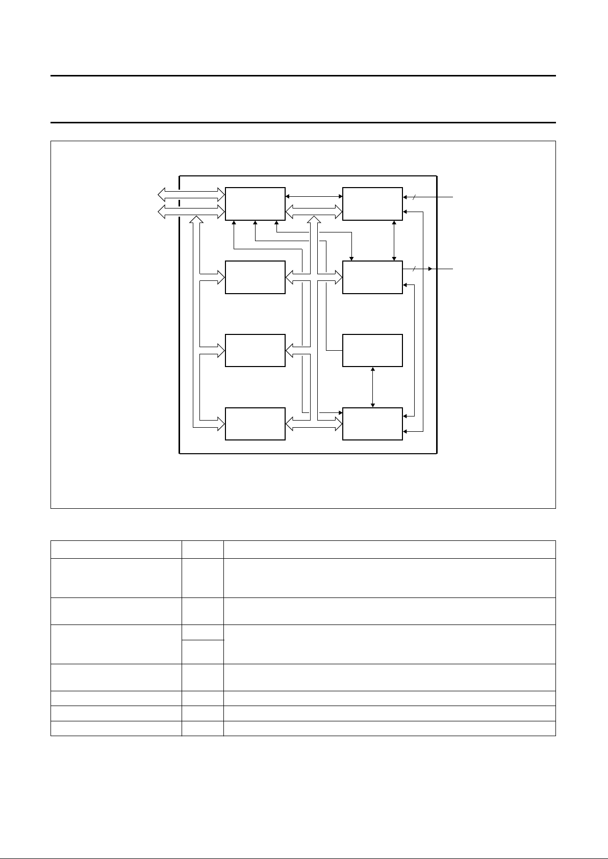
13.3 Interface between CPU and CAN
The internal interface between the P8xC592's CPU and
on-chip CAN-controller is achieved via the following four
SFRs (see Fig.13):
• CANADR, to point to a register of the CAN-controller
• CANDAT, to read or write data
• CANCON, to read interrupt flags and to write commands
• CANSTA, to read status information and to write DMA
pointer.
Additionally, the DMA-logic allows a high-speed data
exchange between the CAN-controller and the CPU's
on-chip MAIN RAM. For more information, see
Section 13.5.15 “Handling of the CPU-CAN interface”.
13.4 Hardware blocks of the CAN-controller
The P8xC592 CAN-controller contains all necessary
hardware for high performance serial network
communications (see Fig.14 and Table 29).
It controls the communication flow through the area
network using the CAN-protocol. The CAN-controller
meets the following automotive requirements:
• Short message length
• Bus access priority, determined by the message
identifier
• Powerful error handling capability
• Configuration flexibility to allow area network expansion
• Guaranteed latency time for urgent messages;
– The latency time defines the period between the
initiation (Transmission Request) and the start of the
transmission on the bus. The latency time strongly
depends on a large variety of bus-related conditions.
In the case of a message being transmitted on the
bus and one distortion, the latency time can be up to
149 bit times (worst case). For more information see
Chapter 22 “CAN application information”.
handbook, full pagewidth
CANADR
DBH
CANDAT
DAH
CANCON
D9H
CANSTA
D8H
ADDRESS
DATA
CAN
CONTROLLER
MAIN
RAM
CPU
DMA
LOGIC
internal
bus
4 special function
registers
MGA158
DMA bus
Fig.13 Interface between CPU and CAN-controller.
Page 29
1996 Jun 27 29
Philips Semiconductors Product specification
8-bit microcontroller with on-chip CAN P8xC592
Table 29 Hardware blocks of the CAN-controller (see Fig.14)
NAME BLOCK DESCRIPTION
Interface Management Logic IML Interprets commands from the CPU, allocates the message buffers
(TBF, RBF0 and RBF1) and provides interrupts and status information to the
microcontroller.
Transmit Buffer TBF 10 bytes memory into which the CPU writes messages which are to be
transmitted over the CAN network.
Receive Buffers (0 and 1) RBF0 RBF0 and RBF1 are each 10 bytes memories which are alternatively used to
store messages received from the CAN network.
The CPU can process one message while another is being received.
RBF1
Bit Stream Processor BSP Is a sequencer, controlling the data stream between the Transmit Buffer,
Receive Buffers (parallel data) and the CAN-bus (serial data).
Bit Timing Logic BTL Synchronizes the CAN-controller to the bitstream on the CAN-bus.
Transceiver Control Logic TCL Controls the output driver.
Error Management Logic EML Performs the error confinement according to the CAN-protocol.
Fig.14 Block diagram of the P8xC592 on-chip CAN-controller.
handbook, full pagewidth
MGA159
INTERFACE
MANAGEMENT
LOGIC
TRANSCEIVER
LOGIC
TRANSMIT
BUFFER
BIT TIMING
LOGIC
2
2
ON - CHIP
CAN
CONTROLLER
RECEIVE
BUFFER 0
RECEIVE
BUFFER 1
BIT STREAM
PROCESSOR
ERROR
MANAGEMENT
LOGIC
address
data
CRX0
and
CRX1
CTX0
and
CTX1
Page 30
1996 Jun 27 30
Philips Semiconductors Product specification
8-bit microcontroller with on-chip CAN P8xC592
13.5 Control Segment and Message Buffer
description
The CAN-controller appears to the CPU as a
memory-mapped peripheral, guaranteeing the
independent operation of both parts.
13.5.1 A
DDRESS ALLOCATION
The address area of the CAN-controller consists of the
Control Segment and the message buffers. The Control
Segment is programmed during an initialization down-load
in order to configure communication parameters (e.g. bit
timing). The communication over the CAN-bus is also
controlled via this segment by the CPU. A message which
is to be transmitted, must be written to the Transmit Buffer.
After a successful reception the CPU may read the
message from the Receive Buffer and then release it for
further use.
13.5.2 CONTROL SEGMENT LAYOUT
The exchange of status, control and command signals
between the CPU and the CAN-controller is performed in
the control segment. The layout of this segment is shown
in Fig.15. After an initial down-load, the contents of the
registers Acceptance Code, Acceptance Mask,
Bus Timing 0, Bus Timing 1 and Output Control should not
be changed. These registers may only be accessed when
the Reset Request bit in the Control Register is set HIGH
(see Tables 30, 31 and 32).
handbook, full pagewidth
ADDRESS
0
control segment
MGA160 - 1
CONTROL
descriptor
data field
transmit buffer
descriptor
data field
receive buffer 0 or 1
1 COMMAND
2 STATUS
3 INTERRUPT
4 ACCEPTANCE CODE
5 ACCEPTANCE MASK
6 BUS TIMING 0
7 BUS TIMING 1
8 OUTPUT CONTROL
9 TEST
10 IDENTIFIER,
11 RTR BIT, DATA LENGTH CODE
12 BYTE 1
13 BYTE 2
14 BYTE 3
15 BYTE 4
16 BYTE 5
17 BYTE 6
18 BYTE 7
19 BYTE 8
2014H
15H
16H
11H
12H
13H
17H
18H
19H
1AH
1BH
1CH
1DH
IDENTIFIER,
21 RTR BIT, DATA LENGTH CODE
22 BYTE 1
23 BYTE 2
24 BYTE 3
25 BYTE 4
26 BYTE 5
27 BYTE 6
28 BYTE 7
29 BYTE 8
IDENTIFIER,
RTR BIT, DATA LENGTH CODE
BYTE 1
BYTE 2
BYTE 3
BYTE 4
BYTE 5
BYTE 6
BYTE 7
BYTE 8
00H
01H
02H
03H
04H
05H
06H
07H
08H
09H
0AH
0CH
0DH
0EH
0FH
10H
0BH
Fig.15 CAN-controller internal address allocation.
Page 31

1996 Jun 27 31
Philips Semiconductors Product specification
8-bit microcontroller with on-chip CAN P8xC592
Table 30 CPU/CAN Register map
BIT
76543210
Control Segment
ADDRESS 0: CONTROL REGISTER
TM S RA OIE EIE TIE RIE RR
ADDRESS 1: COMMAND REGISTER
RX0A RX1A WUM SLP COS RRB AT TR
ADDRESS 2: STATUS REGISTER
BS ES TS RS TCS TBS DO RBS
ADDRESS 3: INTERRUPT REGISTER
Reserved Reserved Reserved WUI OI EI TI RI
ADDRESS 4: ACCEPTANCE CODE REGISTER
AC.7 AC.6 AC.5 AC.4 AC.3 AC.2 AC.1 AC.0
ADDRESS 5: ACCEPTANCE MASK REGISTER
AM.7 AM.6 AM.5 AM.4 AM.3 AM.2 AM.1 AM.0
ADDRESS 6: BUS TIMING REGISTER 0
SJW.1 SJW.0 BRP.5 BRP.4 BRP.3 BRP.2 BRP.1 BRP.0
ADDRESS 7: BUS TIMING REGISTER 1
SAM TSEG2.2 TSEG2.1 TESG2.0 TSEG1.3 TSEG1.2 TSEG1.1 TSEG1.0
ADDRESS 8: OUTPUT CONTROL REGISTER
OCTP1 OCTN1 OCPOL1 OCTP0 OCTN0 OCPOL0 OCMODE1 OCMODE0
ADDRESS 9: TEST REGISTER (note 1)
Reserved Reserved Map Internal
Register
Connect RX
Buffer 0
CPU
Connect TX
Buffer CPU
Access
Internal Bus
Normal
RAM
Connect
Float Output
Driver
Page 32

1996 Jun 27 32
Philips Semiconductors Product specification
8-bit microcontroller with on-chip CAN P8xC592
Note
1. The Test Register is used for production testing only.
13.5.3 C
ONTROL REGISTER (CR)
The contents of the Control Register are used to change the behaviour of the CAN-controller. Control bits may be set or
reset by the CPU which uses the Control Register as a read/write memory.
Table 31 Control Register (address 0)
Table 32 Description of the CR bits
Transmit Buffer
ADDRESS 10: IDENTIFIER
ID.10 ID.9 ID.8 ID.7 ID.6 ID.5 ID.4 ID.3
ADDRESS 11: RTR, DATA LENGTH CODE
ID.2 ID.1 ID.0 RTR DLC.3 DLC.2 DLC.1 DLC.0
ADDRESS 12 TO 19: BYTES 1 TO 8
Data Data Data Data Data Data Data Data
Receive Buffer 0 and 1
ADDRESS 20: IDENTIFIER
ID.10 ID.9 ID.8 ID.7 ID.6 ID.5 ID.4 ID.3
ADDRESS 21: RTR, DATA LENGTH CODE
ID.2 ID.1 ID.0 RTR DLC.3 DLC.2 DLC.1 DLC.0
ADDRESS 22 TO 29: BYTES 1 TO 8
Data Data Data Data Data Data Data Data
76543210
TM S RA OIE EIE TIE RIE RR
BIT SYMBOL FUNCTION
7TM Test Mode (note 1).If the value of TM is:
HIGH (enabled), then the CAN-controller enters Test Mode (normal operations
impossible).
LOW (disabled), then the CAN-controller is in normal operating mode.
6S Sync (note 2). If the value of S is:
HIGH (2 edges), then bus-line transitions from recessive-to-dominant and vice-versa
are used for resynchronization (see Sections 13.5.20 and 13.6).
LOW (1 edge), then the only transitions from recessive-to-dominant are used for
resynchronization.
BIT
76543210
Page 33

1996 Jun 27 33
Philips Semiconductors Product specification
8-bit microcontroller with on-chip CAN P8xC592
Notes to the description of the CR bits
1. The test mode is intended for factory testing and not for customer use.
2. A modification of the bits Reference Active and Sync is only possible with Reset Request = HIGH (present). It is
allowed to set these bits while Reset Request is changed from a HIGH level to a LOW level. After an external reset
(pin RST = HIGH) the Reference Active bit is set HIGH (output), the Sync bit is undefined.
3. During an external reset (RST = HIGH) or when the Bus Status bit is set HIGH (Bus-OFF), the IML forces the
Reset Request HIGH (present). After the Reset Request bit is set LOW (absent) the CAN-controller will wait for:
a) One occurrence of the Bus-Free signal (11 recessive bits, see Section 13.6.9.6), if the preceding reset (Reset
Request = HIGH) has been caused by an external reset or a CPU initiated reset.
b) 128 occurrences of Bus-Free, if the preceding reset (Reset Request = HIGH) has been caused by a
CAN-controller initiated Bus-OFF, before re-entering the Bus-On mode, see Section 13.6.9.
c) When Reset Request is set HIGH (present), for whatever reason, the Control, Command, Status and Interrupt
bits are affected, see Table 40. The registers at addresses 4 to 8 are only accessible when the Reset Request is
set HIGH (present).
5RA Reference Active (notes 2). If the value of RA is:
HIGH (output), then the pin REF is an1⁄2AVDD reference output.
LOW (input), then a reference voltage may be input.
4 OIE Overrun Interrupt Enable. If the value of OIE is:
HIGH (enabled) and the Data Overrun bit is set (see Section 13.5.5) then the CPU
receives an Overrun Interrupt signal.
LOW (disabled), then the CPU receives no Overrun Interrupt signal from the
CAN-controller.
3 EIE Error Interrupt Enable. If the value of EIE is:
HIGH (enabled) and the Error or Bus Status change (see Section 13.5.5) then the CPU
receives an Error Interrupt signal.
LOW (disabled), then the CPU receives no Error Interrupt signal.
2 TIE Transmit Interrupt Enable. If the value of TIE is:
HIGH (enabled) and when a message has been successfully transmitted or the
Transmit Buffer is accessible again, (e.g. after an Abort Transmission command), then
the CAN-controller transmits a Transmit Interrupt signal to the CPU.
LOW (disabled), then there is no transmission of the Transmit Interrupt signal by the
CAN-controller to the CPU.
1 RIE Receive Interrupt Enable. If the value of RIE is:
HIGH (enabled) and when a message has been received without errors, then the
CAN-controller transmits a Receive Interrupt signal to the CPU.
LOW (disabled), then there is no transmission of the Receive Interrupt signal by the
CAN-controller to the CPU.
0RR Reset Request (note 3). If the value of RR is:
HIGH (present), then detection of a Reset Request results in the CAN-controller
aborting the current transmission/reception of a message entering the reset state
synchronously to the system clock (t
SCL
, see Section 13.5.9).
LOW (absent), on the HIGH-to-LOW transition of the Reset Request bit, the
CAN-controller returns to its normal operating state.
BIT SYMBOL FUNCTION
Page 34

1996 Jun 27 34
Philips Semiconductors Product specification
8-bit microcontroller with on-chip CAN P8xC592
handbook, full pagewidth
MGA161
single-ended
wake-up
WAKE-UP
(bus active signal)
COMP OUT
RX0 ACTIVE
RX1 ACTIVE
1/2 AV - VOLTAGE
WAKE-UP MODE
1
0
S2
RX0
RX1
1
0
S1
0
1
S0
differential
wake-up
P8xC592
REF
CRX0
CRX1
REFERENCE ACTIVE
DD
Fig.16 Configurable CAN receiver.
Page 35

1996 Jun 27 35
Philips Semiconductors Product specification
8-bit microcontroller with on-chip CAN P8xC592
13.5.4 COMMAND REGISTER (CMR)
A command bit initiates an action within the transfer layer of the CAN-controller. The Command Register appears to the
CPU as a read/write memory, except for the bits CMR.0 (TR) to CMR.3 (COS), which return a HIGH if being read.
Table 33 Command Register (address 1)
Table 34 Description of the CMR bits
76543210
RX0A RX1A WUM SLP COS RRB AT TR
BIT SYMBOL FUNCTION
7 RX0A RX0 Active. See Table 35; note 1.
6 RX1A RX1 Active. See Table 35; note 1.
5 WUM Wake-up Mode (note 2). If the value of WUM is:
HIGH (single ended), then the difference of the RX signals to the internal reference voltage
1
⁄2AV
DD
is used for wake up.
LOW (differential), then the differential signal between RX0 and RX1 is used for wake up.
4 SLP Sleep (note 3). If the value of SLP is:
HIGH (sleep), then the CAN-controller enters sleep mode if no CAN interrupt is pending and there
is no bus activity.
LOW (wake up), then the CAN-controller functions normally.
3 COS Clear Overrun Status (note 4). If the value of COS is:
HIGH (clear), then the Data Overrun status bit is set to LOW (see Table 37).
LOW (no action), then there is no action.
2 RRB Release Receive Buffer (note 5). If the value of RRB is:
HIGH (released), then the Receive Buffer attached to the CPU is released.
LOW (no action), then there is no action.
1AT Abort Transmission (note 6). If the value of AT is:
HIGH (present) and if not already in progress, a pending Transmission Request is cancelled.
LOW (absent), then there is no action.
0TR Transmission Request (note 7). If the value of TR is:
HIGH (present), then a message shall be transmitted.
LOW (absent), then there is no action.
Page 36

1996 Jun 27 36
Philips Semiconductors Product specification
8-bit microcontroller with on-chip CAN P8xC592
Notes to the description of the CMR bits
1. The RX0/RX1 Active bits, if being read, reflect the status of the respective switches (see Fig.16). It is recommended
to change the switches only during the reset state (Reset Request = HIGH).
2. The Wake-Up Mode bit should be set at the same time as the Sleep bit. The differential wake up mode is useful if
both bus wires are fully functioning; it minimizes the amount of wake ups due to noise. The single ended wake up
mode is recommended if a wake up must be possible even if one bus wire is already or may become disturbed
(see Fig.16).
3. The CAN-controller will enter sleep mode, if the Sleep bit is set HIGH (sleep) there is no bus activity and no interrupt
is pending. The CAN-controller will wake up after the Sleep bit is set LOW (wake up) or when there is bus activity.
On wake up, a Wake-Up Interrupt (see Section 13.5.6) is generated (see also Chapter 15). A CAN-controller which
is sleeping and then awaken by bus activity will not be able to receive this message until it detects a Bus-Free signal
(see Section 13.6.9.6). The Sleep bit, if read, reflects the status of the CAN-controller.
4. This command bit is used to acknowledge the Data Overrun condition signalled by the Data Overrun status bit.
Command is given only after releasing both receive buffers. The stored messages have to be rejected. The
command bit is set simultaneously with setting of the Release Receive Buffer command bit the second time.
5. After reading the contents of the Receive Buffer (RBF0 or RBF1) the CPU must release this buffer by setting Release
Receive Buffer bit HIGH (released). This may result in another message becoming immediately available.
To prevent the RRB command being executed only once, the minimum wait time between two successive RRB
commands is 3 system clock cycles (t
SCL
, see Section 13.5.9).
6. The Abort Transmission bit is used when the CPU requires the suspension of the previously requested transmission,
e.g. to transmit an urgent message. A transmission already in progress is not stopped. In order to see if the original
message had been either transmitted successfully or aborted, the Transmission Complete Status bit should be
checked. This should be done after the Transmit Buffer Access bit has been set HIGH (released) or a Transmit
Interrupt has been generated (see Section 13.5.6).
7. If the Transmission Request bit was set HIGH in a previous command, it cannot be cancelled by setting the
Transmission Request bit LOW (absent). Cancellation of the requested transmission may be performed by setting
the Abort Transmission bit HIGH (present).
Table 35 Combination of bits RX0A and RX1A (see Fig.16)
CONTROL
RX0 RX1
RX0A RX1A
1 1 CRX0 CRX1
1 0 CRX0
1
⁄2AV
DD
01
1
⁄
2
AV
DD
CRX1
0 0 No action
Page 37

1996 Jun 27 37
Philips Semiconductors Product specification
8-bit microcontroller with on-chip CAN P8xC592
13.5.5 STATUS REGISTER (SR)
The contents of the Status Register reflects the status of the CAN-controller. The Status Register appears to the CPU
as a read only memory.
Table 36 Status Register (address 2)
Table 37 Description of the SR bits
76543210
BS ES TS RS TCS TBS DO RBS
BIT SYMBOL FUNCTION
7BS Bus Status (note 1). If the value of BS is:
HIGH (Bus-OFF), then the CAN-controller is not involved in bus activities.
LOW (Bus-ON), then the CAN-controller is involved in bus activities.
6ES Error Status. If the value of ES is:
HIGH (error), then at least one of the Error Counters (see Section 13.6.10) has reached the
CPU Warning limit.
LOW (ok), then both Error Counters have not reached the warning limit.
5TS Transmit Status (note 2). If the value of TS is:
HIGH (transmit), then the CAN-controller is transmitting a message.
LOW (idle), then no message is transmitted.
4RS Receive Status (note 2). If the value of RS is:
HIGH (receive), then the CAN-controller is receiving a message.
LOW (idle), then no message is received.
3 TCS Transmission Complete Status (note 3). If the value of TCS is:
HIGH (complete), then last requested transmission has been successfully completed.
LOW (incomplete), then previously requested transmission is not yet completed.
2 TBS Transmit Buffer Access (note 3). If the value of TBS is:
HIGH (released), then the CPU may write a message into the TBF.
LOW (locked), then the CPU cannot access the Transmit Buffer. A message is either waiting for
transmission or is in the process of being transmitted.
1DO Data Overrun (note 4). If the value of DO is:
HIGH (overrun), then both Receive Buffers are full and the first byte of another message should be
stored.
LOW (absent), then no data overrun has occurred since the Clear Overrun command was given.
0 RBS Receive Buffer Status (note 5). If the value of RBS is
HIGH (full), then this bit is set when a new message is available.
LOW (empty), then no message has become available since the last Release Receive Buffer
command bit was set.
Page 38

1996 Jun 27 38
Philips Semiconductors Product specification
8-bit microcontroller with on-chip CAN P8xC592
Notes to the description of the SR bits
1. When the Bus Status bit is set HIGH (Bus-OFF), the CAN-controller will set the Reset Request bit HIGH (present).
It will stay in this state until the CPU sets the Reset Request bit LOW (absent). Once this is completed the
CAN-controller will wait the minimum protocol-defined time (128 occurrences of the Bus-Free signal) before setting
the Bus Status bit LOW (Bus-ON), the Error Status bit LOW (ok) and resetting the Error Counters. During Bus-OFF
the output drivers are switched off (floating); external transceiver circuits should output a recessive level in this case.
2. If both the Receive Status and Transmit Status bits are LOW (idle) the CAN-bus is idle.
3. If the CPU tries to write to the Transmit Buffer when the Transmit Buffer Access bit is LOW (locked), the written bytes
will not be accepted and will be lost without this being signalled. The Transmission Complete Status bit is set LOW
(incomplete) whenever the Transmission Request bit is set HIGH (present). If an Abort Transmission command is
issued, the Transmit Buffer will be released. If the message, which was requested and then aborted, was not
transmitted, the Transmission Complete Status bit will remain LOW.
4. If Data Overrun = HIGH (overrun) is detected, the currently received message is dropped. A transmitted message,
granted acceptance, is also stored in a Receive Buffer. This occurs because it is not known if the CAN-controller will
lose arbitration and so become a receiver of the message. If no Receive Buffer is available, Data Overrun is
signalled. However, this transmitted and accepted message does neither cause a Receive Interrupt nor set the
Receive Buffer Status bit to HIGH (full). Also, a Data Overrun does not cause the transmission of an Overload Frame
(see Sections 13.6.1 and 13.6.5).
5. If the command bit Release Receive Buffer is set HIGH (released) by the CPU, the Receive Buffer Status bit is set
LOW (empty) by IML. When a new message is stored in any of the receive buffers, the Receive Buffer Status bit is
set HIGH (full) again.
Page 39

1996 Jun 27 39
Philips Semiconductors Product specification
8-bit microcontroller with on-chip CAN P8xC592
13.5.6 INTERRUPT REGISTER (IR)
The Interrupt Register allows the identification of an interrupt source. When one or more bits of this register are set, a
CAN interrupt (SI01) will be indicated to the CPU. All bits are reset by the CAN-controller after this register is read by the
CPU. This register appears to the CPU as a read only memory.
Table 38 Interrupt Register (address 3)
Table 39 Description of the IR bits
Notes
1. Overrun Interrupt bit (if enabled) and Data Overrun bit (see Section 13.5.5) are set at the same time.
2. Receive Interrupt bit (if enabled) and Receive Buffer Status bit (see Section 13.5.5) are set at the same time.
76543210
−−−WUI OI EI TI RI
BIT SYMBOL FUNCTION
7 − Reserved.
6 − Reserved.
5 − Reserved.
4 WUI Wake-Up Interrupt. The value of WUI is set to:
HIGH (set), when the sleep mode is left. See Section 13.5.4.
LOW (reset), by a read access of the Interrupt Register by the CPU.
3OI Overrun Interrupt (note 1). The value of OI is set to:
HIGH (set), if both Receive Buffers contain a message and the first byte of another message should
be stored (passed acceptance), and the Overrun Interrupt Enable is HIGH (enabled).
LOW (reset), by a read access of the Interrupt Register by the CPU.
2EI Error Interrupt. The value of EI is set to:
HIGH (set), on a change of either the Error Status or Bus Status bits, if the Error Interrupt Enable is
HIGH (enabled). See Section 13.5.5.
LOW (reset), by a read access of the Interrupt Register by the CPU.
1TI Transmit Interrupt. The value of TI is set to:
HIGH (set), on a change of the Transmit Buffer Access from LOW to HIGH (released) and
Transmit Interrupt Enable is HIGH (enabled).
LOW (reset), after a read access of the Interrupt Register by the CPU.
0RI Receive Interrupt (note 2). The value of RBS is set to:
HIGH (set), when a new message is available in the Receive Buffer and the Receive Interrupt
Enable bit is HIGH (enabled).
LOW (reset) automatically by a read access of Interrupt Register by the CPU.
Page 40

1996 Jun 27 40
Philips Semiconductors Product specification
8-bit microcontroller with on-chip CAN P8xC592
Table 40 Effects of setting the Reset Request bit HIGH (present)
Note
1. Only after an external reset; see note 5 to Table 37 “Description of the SR bits”.
TYPE BIT SYMBOL FUNCTION EFFECT
Control CR.7 TM Test Mode LOW (disabled)
CR.5 RA Reference Active HIGH (output); note 1
Command CMR.7 RX0A RX0 Active HIGH (RX0 = CRX0); note 1
CMR.6 RX1A RX1 Active HIGH (RX1 = CRX1); note 1
CMR.4 SLP Sleep LOW (wake-up)
CMR.3 COS Clear Overrun Status HIGH (clear)
CMR.2 RRB Release Receive Buffer HIGH (released)
CMR.1 AT Abort Transmission LOW (absent)
CMR.0 TR Transmission Request LOW (absent)
Status SR.7 BS Bus Status LOW (Bus-On); note 1
SR.6 ES Error Status LOW (no error); note 1
SR.5 TS Transmit Status LOW (idle)
SR.4 RS Receive Status LOW (idle)
SR.3 TCS Transmission Complete Status HIGH (complete)
SR.2 TBS Transmit Buffer Access HIGH (released)
SR.1 DO Data Overrun LOW (absent)
SR.0 RBS Receive Buffer Status LOW (empty)
Interrupt IR.3 OI Overrun Interrupt LOW (reset)
IR.1 TI Transmit Interrupt LOW (reset)
IR.0 RI Receive Interrupt LOW (reset)
Page 41

1996 Jun 27 41
Philips Semiconductors Product specification
8-bit microcontroller with on-chip CAN P8xC592
13.5.7 ACCEPTANCE CODE REGISTER (ACR)
The Acceptance Code Register is part of the acceptance
filter of the CAN-controller. This register can be accessed
(read/write), if the Reset Request bit is set HIGH (present).
When a message is received which passes the
acceptance test and if there is an empty Receive Buffer,
then the respective Descriptor and Data Field
(see Fig.15) are sequentially stored in this empty buffer.
In the event that there is no empty Receive Buffer, the
Data Overrun bit is set HIGH (overrun); see
Sections 13.5.5 and 13.5.6.
When the complete message has been correctly received
the following occurs:
• The Receive Buffer Status bit is set HIGH (full)
• If the Receive Interrupt Enable bit is set HIGH (enabled),
the Receive Interrupt is set HIGH (set).
During transmission of a message which passes the
acceptance test, the message is also written to its own
Receive Buffer. If no Receiver Buffer is available, Data
Overrun is signalled because it is not known at the start of
a message whether the CAN-controller will lose arbitration
and so become a receiver of the message.
Table 41 Acceptance Code Register (address 4)
Table 42 Description of the ACR bits
76543210
AC.7 AC.6 AC.5 AC.4 AC.3 AC.2 AC.1 AC.0
BIT SYMBOL FUNCTION
7
to
0
AC.7
to
AC.0
Acceptance Code. The Acceptance Code bits (AC.7 to AC.0) and the eight most significant
bits of the message's Identifier (ID.10 to ID.3) must be equal to those bit positions which are
marked relevant by the Acceptance Mask bits (AM.7 to AM.0).
The acceptance is given, if the following equation is satisfied:
(ID10 ... ID.3) = [(AC.7 ... AC.0) or (AM.7 ... AM.0)] = 1111 1111 B.
13.5.8 ACCEPTANCE MASK REGISTER (AMR)
The Acceptance Mask Register is part of the acceptance
filter of the CAN-controller.
This register can be accessed (read/write) if the Reset
Request bit is set HIGH (present).
The Acceptance Mask Register qualifies which of the
corresponding bits of the acceptance code are ‘relevant’ or
‘don't care’ for acceptance filtering.
Table 43 Acceptance Mask Register (address 5)
Table 44 Description of the AMR bits
76543210
AM.7 AM.6 AM.5 AM.4 AM.3 AM.2 AM.1 AM.0
BIT SYMBOL FUNCTION
7
to
0
AM.7
to
AM.0
Acceptance Mask. If the Acceptance Mask bit is:
HIGH (don’t care), then this bit position is ‘don’t care’ for the acceptance of a message.
LOW (relevant), then this bit position is ‘relevant’ for acceptance filtering.
Page 42

1996 Jun 27 42
Philips Semiconductors Product specification
8-bit microcontroller with on-chip CAN P8xC592
13.5.9 BUS TIMING REGISTER 0 (BTR0)
The contents of Bus Timing Register 0 defines the values
of the Baud Rate Prescaler (BRP) and the Synchronization
Jump Width (SJW).
This register can be accessed (read/write) if the Reset
Request bit is set HIGH (present).
For further information on bus timing, see
Sections 13.5.10 and 13.5.18.
Table 45 Bus Timing Register 0 (address 6)
Table 46 Description of the BTR0 bits
76543210
SJW.1 SJW.0 BRP.5 BRP.4 BRP.3 BRP.2 BRP.1 BRP.0
BIT SYMBOL FUNCTION
7 SJW.1
Synchronization Jump Width. To compensate for phase shifts between clock oscillators of different
bus controllers, any bus controller must resynchronize on any relevant signal edge of the current
transmission. The synchronization jump width defines the maximum number of clock cycles a bit
period may be shortened or lengthened by one resynchronization:
6 SJW.0
5 BRP.5
Baud Rate Prescaler. The period of the system clock t
SCL
is programmable and determines the
individual bit timing.The system clock is calculated using the following equation:
.
Where t
CLK
= time period of the P8xC592 oscillator.
4 BRP.4
3 BRP.3
2 BRP.2
1 BRP.1
0 BRP.0
t
SJWtSCL
2SJW.1 SJW.0 1++().
˙˙
=
t
SCL
2t
CLK
32BRP.5 16BRP.4 8BRP.3 4BRP.2 2BRP.1 BRP.0 1+ +++++()=
Page 43

1996 Jun 27 43
Philips Semiconductors Product specification
8-bit microcontroller with on-chip CAN P8xC592
13.5.10 BUS TIMING REGISTER 1(BTR1)
The contents of Bus Timing Register 1 defines the length
of the bit period, the location of the sample point and the
number of samples to be taken at each sample point.
This register can be accessed (read/write) if the Reset
Request bit is set HIGH (present).For further information
on bus timing, see Sections 13.5.9 and 13.5.18.
Table 47 Bus Timing Register 1 (address 7)
Table 48 Description of the BTR1 bits
76543210
SAM TSEG2.2 TSEG2.1 TSEG2.0 TSEG1.3 TSEG1.2 TSEG1.1 TSEG1.0
BIT SYMBOL FUNCTION
7 SAM Sampling. If the bit SAM is:
HIGH (3 samples), then three samples are taken. This is recommended for slow/medium speed
buses (SAE class A and B) where filtering of spikes on the bus-line is beneficial
(see Section 13.5.19.6)
LOW (1 sample), the bus is sampled once.
This is recommended for high speed buses (SAE class C).
6 TSEG2.2
Time Segment 1 (TSEG1) and Time Segment 2 (TSEG2).
TSEG1 determines the number of clock cycles per bit period and the location of the sample point
.
TSEG2 determines the number of clock cycles per bit period and the location of the sample point:
.
5 TSEG2.1
4 TSEG2.0
3 TSEG1.3
2 TSEG1.2
1 TSEG1.1
0 TSEG1.0
t
TSEG1tSCL
8TSEG1.3 4TSEG1.2 2TSEG1.1 TSEG1.0 1++++()=
t
TSEG2tSCL
4TSEG2.2 2TSEG2.1 TSEG2.0 1+++()=
Page 44

1996 Jun 27 44
Philips Semiconductors Product specification
8-bit microcontroller with on-chip CAN P8xC592
13.5.11 OUTPUT CONTROL REGISTER (OCR)
The Output Control Register allows, under software
control, the set-up of different output driver configurations.
This register can be accessed (read/write) if the Reset
Request bit is set HIGH (present). If the CAN-controller is
in the sleep mode (Sleep = HIGH) a recessive level is
output on the CTX0 and CTX1 pins. If the CAN-controller
is in the reset state (Reset Request = HIGH) the output
drivers are floating.
Tables 50 and 51, show the relationship between the bits
of the Output Control Register and the two serial output
pins CTX0 and CTX1 of the P8xC592 CAN-controller,
connected to the serial bus (see Fig.14).
Table 49 Output Control Register (address 8)
Table 50 Description of the OCR bits
Table 51 Description of the Output Mode bits
76543210
OCTP1 OCTN1 OCPOL1 OCTP0 OCTN0 OCPOL0 OCMODE1 OCMODE0
BIT SYMBOL FUNCTION
7 OCTP1 See Tables 51 and 52.
6 OCTN1
5 OCPOL1
4 OCTP0
3 OCTN0
2 OCPOL0
1 OCMODE1 Output Mode.
These bits select the output mode; see Table 51.
0 OCMODE0
OCMODE1 OCMODE0 DESCRIPTION
10Normal Output Mode. The bit sequence (TXD) is sent via CTX0, CTX1. TXD is the data
bit to be transmitted. The voltage levels on the output driver pins CTX0 and CTX1 depend
on both the driver characteristic programmed by OCTPx, OCTNx (float, pull-up, pull-down,
push-pull) and the output polarity programmed by OCPOLx (see Fig.17).
11Clock Output Mode. For the CTX0 pin this is the same as in Normal Output Mode
(CTX0: bit sequence). However, the data stream to CTX1 is replaced by the transmit clock
(TXCLK). The rising edge of the transmit clock (non-inverted) marks the beginning of a bit
period. The clock pulse width is t
SCL
.
00Bi-phase Output Mode. In contrast to Normal Output Mode the bit representation is time
variant and toggled. If the bus controllers are galvanically decoupled from the bus-line by a
transformer, the bit stream is not allowed to contain a DC component. This is achieved by
the following scheme. During recessive bits all outputs are deactivated (floating). Dominant
bits are sent alternately on CTX0 and CTX1, i.e. the first dominant bit is sent on CTX0, the
second is sent on CTX1, and the third one is sent on CTX0 again, etc.
01Test Output Mode. For the CTX0 pin this is the same as in Normal Output Mode
(CTX0: bit sequence). To measure the delay time of the transmitter and receiver this mode
connects the output of the input comparator (COMP OUT) with the input of the output driver
CTX1. This mode is used for production testing only.
Page 45

1996 Jun 27 45
Philips Semiconductors Product specification
8-bit microcontroller with on-chip CAN P8xC592
Table 52 Output pin set-up
Notes
1. TPx is the on-chip output transistor x, connected to VDD; x=0or1.
2. TNx is the on-chip output transistor x, connected to CVSS; x = 0 or 1.
3. CTXx is the serial output level on CTX0 or CTX1. It is required that the output level on the CAN-bus is dominant with
TXD = 0 and recessive with TXD = 1, see Section 13.6.1.1 “Bit representation”.
DRIVE OCTPx OCTNx OCPOLx TXD TPx
(1)
TNx
(2)
CTXx
(3)
Float 0 0 0 0 OFF OFF float
0 0 0 1 OFF OFF float
0 0 1 0 OFF OFF float
0 0 1 1 OFF OFF float
Pull-down 0 1 0 0 OFF ON LOW
0 1 0 1 OFF OFF float
0 1 1 0 OFF OFF float
0 1 1 1 OFF ON LOW
Pull-up 1 0 0 0 OFF OFF float
1 0 0 1 ON OFF HIGH
1 0 1 0 ON OFF HIGH
1 0 1 1 OFF OFF float
Push/Pull 1 1 0 0 OFF ON LOW
1 1 0 1 ON OFF HIGH
1 1 1 0 ON OFF HIGH
1 1 1 1 OFF ON LOW
handbook, full pagewidth
MGA162
TP0
TN0
V
DD
TP1
TN1
V
DD
CV
SS
OUTPUT
CONTROL
LOGIC
OCTN1 OCTN0
OCTP1 OCTP0
OCPOL0
OCPOL1
OCMODE0
OCMODE1
TXD
TXCLK
CTX0
CTX1
CV
SS
Fig.17 Configurable CAN Transmitter.
Page 46

1996 Jun 27 46
Philips Semiconductors Product specification
8-bit microcontroller with on-chip CAN P8xC592
13.5.12 TEST REGISTER (TR)
The Test Register is used for production testing only.
Table 53 Test Register (address 9)
13.5.13 T
RANSMIT BUFFER LAYOUT
The global layout of the Transmit Buffer is shown in Fig.15. This buffer serves to store a message from the CPU to be
transmitted by the CAN-controller. It is subdivided into Descriptor and Data Field. The Transmit Buffer can be written to
and read from by the CPU.
13.5.13.1 Descriptor
Table 54 Descriptor Byte 1 Register (DSCR1, address 10)
Table 55 Descriptor Byte 2 Register (DSCR2, address 11)
Table 56 Description of the ID.n bits in DSCR1 and DSCR2
76543210
Reserved Reserved Map Internal
Register
Connect RX
Buffer 0
CPU
Connect TX
Buffer CPU
Access
Internal Bus
Normal
RAM
Connect
Float Output
Driver
76543210
ID.10 ID.9 ID.8 ID.7 ID.6 ID.5 ID.4 ID.3
76543210
ID.2 ID.1 ID.0 RTR DLC.3 DLC.2 DLC.1 DLC.0
BIT SYMBOL FUNCTION
DSCR1
7 ID.10 Identifier. The Identifier consists of 11 bits (ID.10 to ID.0). ID.10 is the most significant
bit, which is transmitted first on the bus during the arbitration process. The Identifier acts
as the messages' name, used in a receiver for acceptance filtering, and also determines
the bus access priority during the arbitration process. The lower the binary value of the
Identifier the higher the priority . This is due to the larger number of leading dominant bits
during arbitration (see Section 13.6.7).
6 ID.9
5 ID.8
4 ID.7
3 ID.6
2 ID.5
1 ID.4
0 ID.3
DSCR2
7 ID.2 Identifier. See DSCR1.
6 ID.1
5 ID.0
Page 47

1996 Jun 27 47
Philips Semiconductors Product specification
8-bit microcontroller with on-chip CAN P8xC592
Table 57 Description of the other DSCR2 bits
BIT SYMBOL FUNCTION
4RTR Remote Transmission Request. If the RTR bit is:
HIGH (remote), then the Remote Frame will be transmitted by the CAN-controller.
LOW (data), then the Data Frame will be transmitted by the CAN-controller.
3 DLC.3
Data Length Code (DLC). The number of bytes (Data Byte Count) in the Data Field of a message is
coded by the Data Length Code. At the start of a Remote Frame transmission the Data Length Code
is not considered due to the RTR bit being HIGH (remote). This forces the number of
transmitted/received data bytes to be a logic 0. Nevertheless, the Data Length Code must be
specified correctly to avoid bus errors, if two CAN-controllers start a Remote Frame transmission
simultaneously. The range of the Data Byte Count is 0 to 8 bytes and coded as follows:
.
For reasons of compatibility no Data Byte Counts other than 0,1,2,....8 should be used.
2 DLC.2
1 DLC.1
0 DLC.0
Data Byte Count 8DLC.3 4DLC.2 2DLC.1 DLC.0+++=
13.5.13.2 Data Field
The number of transferred data bytes is determined by the
Data Length Code. The first bit transmitted is the most
significant bit of data byte 1 at address 12.
13.5.14 R
ECEIVE BUFFER LAYOUT
The layout of the Receive Buffer and the individual bytes
correspond to the definitions given for the Transmit Buffer
layout, except that the addresses start at 20 instead of 10
(see Fig.15).
13.5.15 H
ANDLING OF THE CPU-CAN INTERFACE
Via the four special registers CANADR, CANDAT,
CANCON and CANSTA the CPU has access to the
CAN-controller and also to the DMA-logic. Note that
CANCON and CANSTA have different meanings for a
Read and Write access.
Table 58 The SFRs between CPU and CAN
Reserved bits are read as HIGH. R = Read; W = Write; R/W = Read/Write.
ADDRESS ACCESS
BIT
76543210
CANADR
DBH R/W DMA Reserved AutoInc CANA4 CANA3 CANA2 CANA1 CANA0
CANDAT
DAH R/W CAND7 CAND6 CAND5 CAND4 CAND3 CAND2 CAND1 CAND0
CANCON; Do not use a RMW instruction
D9H R Reserved Reserved Reserved WUI OI EI TI RI
W RX0A RX1A WUM SLP COS RRB AT TR
CANSTA; The bit addresses of CANSTA (7 to 0) are DFH to D8H; do not use a RMW instruction
DFH to D8H R BS ES TS RS TCS TBS DO RBS
W RAMA7 RAMA6 RAMA5 RAMA4 RAMA3 RAMA2 RAMA1 RAMA0
Page 48

1996 Jun 27 48
Philips Semiconductors Product specification
8-bit microcontroller with on-chip CAN P8xC592
13.5.15.1 Special Function Register CANADR
CANADR is implemented as a read/write register.
Table 59 SFR CANADR (address DBH)
Table 60 Description of the CANADR bits
13.5.15.2 Special Function Register CANDAT
CANDAT is implemented as a read/write register.
Table 61 SFR CANDAT (addressDAH)
Table 62 Description of the CANADR bits
76543210
DMA − AutoInc CANA4 CANA3 CANA2 CANA1 CANA0
BIT SYMBOL FUNCTION
7 DMA DMA-logic controlled via bit CANADR.7 (see Section 13.5.17).
6 − Reserved.
5 AutoInc Auto Address Increment mode controlled via bit CANADR.5 (see Section 13.5.16).
4 CANA4 The five least significant bits CANADR.4 to CANADR.0 define the address of one of the
CAN-controller internal registers to be accessed via CANDAT. For instance, after an external
hardware (e.g. power-on) reset CANADR contains the value 64H, and hence the CPU accesses
(read/write) the Acceptance Code register of the CAN-controller, via the SFR CANDAT.
3 CANA3
2 CANA2
1 CANA1
0 CANA0
76543210
CAND7 CAND6 CAND5 CAND4 CAND3 CAND2 CAND1 CAND0
BIT SYMBOL FUNCTION
7
to
0
CAND7
to
CAND0
The SFR CANDA T appears as a port to the CAN-controller internal register (memory location) being
selected by CANADR. Reading or writing CANDAT is effectively an access to that CAN-controller
internal register, which is selected by CANADR.
Page 49

1996 Jun 27 49
Philips Semiconductors Product specification
8-bit microcontroller with on-chip CAN P8xC592
13.5.15.3 Special Function Register CANCON
Table 63 SFR CANCON in Read access (address D9H)
Table 64 Description of the CANCON bits in Read access
When reading CANCON the Interrupt Register of the CAN-controller is accessed.
Table 65 SFR CANCON in Write access (address D9H)
Table 66 Description of the CANCON bits in Write access
When writing to CANCON then the Command Register of the CAN-controller is accessed.
76543210
−−−WUI OI EI TI RI
BIT SYMBOL FUNCTION
7 − Reserved; bits are read as HIGH.
6 −
5 −
4 WUI Wake-Up Interrupt (see Table 39).
3 OI Overrun Interrupt (see Table 39).
2 EI Error Interrupt (see Table 39).
1 TI Transmit Interrupt (see Table 39).
0 RI Receive Interrupt (see Table 39).
76543210
RX0A RX1A WUM SLP COS RRB AT TR
BIT SYMBOL FUNCTION
7 RX0A RX0 Active (see Table 34).
6 RX1A RX1 Active (see Table 34).
5 WUM Wake-Up Mode (see Table 34).
4 SLP Sleep (see Table 34).
3 COS Clear Overrun Status (see Table 34).
2 RRB Release Receive Buffer (see Table 34).
1 AT Abort Transmission (see Table 34).
0 TR Transmission Request (see Table 34).
Page 50

1996 Jun 27 50
Philips Semiconductors Product specification
8-bit microcontroller with on-chip CAN P8xC592
13.5.15.4 Special Function Register CANSTA
CANSTA is implemented as a bit-addressable read/write register.
The bit addresses of CANSTA (7 to 0) are DFH to D8H.
Table 67 SFR CANCON in Read access (address DFH to D8H)
Table 68 Description of the CANCON bits in Read access
When reading CANSTA the Status Register of the CAN-controller is accessed.
Table 69 SFR CANCON in Write access (address DFH to D8H)
Table 70 Description of the CANSTA bits inWrite access
Writing to CANSTA sets the address of the on-chip MAIN RAM (internal Data Memory) for a subsequent DMA transfer.
76543210
BS ES TS RS TCS TBS DO RBS
BIT SYMBOL FUNCTION
7 BS Bus Status (see Table 37).
6 ES Error Status (see Table 37).
5 TS Transmit Status (see Table 37).
4 RS Receive Status (see Table 37).
3 TCS Transmission Complete Status (see Table 37).
2 TBS Transmit Buffer Access (see Table 37).
1 DO Data Overrun (see Table 37).
0 RBS Receive Buffer Status (see Table 37).
76543210
RAMA7 RAMA6 RAMA5 RAMA4 RAMA3 RAMA2 RAMA1 RAMA0
BIT SYMBOL FUNCTION
7
to
0
RAMA7
to
RAMA0
−
Page 51

1996 Jun 27 51
Philips Semiconductors Product specification
8-bit microcontroller with on-chip CAN P8xC592
13.5.16 AUTO ADDRESS INCREMENT
With the Auto Address Increment mode a fast stack-like
reading and writing of CAN-controller internal registers is
provided. If the bit CANADR.5 (AutoInc) is HIGH, the
content of CANADR is incremented automatically after any
read or write access to CANDAT. For instance, loading a
message into the Transmit Buffer can be done by writing
2AH into CANADR and then moving byte by byte of the
message to CANDAT. Incrementing CANADR beyond
XX111111B resets the bit CANADR.5 (AutoInc)
automatically (CANADR = XX000000B).
13.5.17 H
IGH SPEED DMA
The DMA-logic allows you to transfer a complete message
(up to 10 bytes) between CAN-controller and MAIN RAM
in 2 instruction cycles at maximum; up to 4 bytes are
transferred in 1 instruction cycle. The performance of the
CPU is strongly enhanced because this very fast transfer
is carried out in the background.
A DMA transfer is achieved by first writing the RAM
address (00H to FFH) into CANSTA and then setting the
TX- or RX-Buffer address in CANDR and the bit
CANADR.7 (DMA) simultaneously; the RAM address
points to the location of the first byte to be transferred.
Setting the DMA bit causes an automatic evaluation of the
Data Length Code and then the transfer; for a TX-DMA
transfer the Data Length Code is expected at the location
‘RAM address +1’.
In order to program a TX-DMA transfer the value 8AH
(address 10) has to be written into CANADR. Then a
complete message, consisting of the 2-byte Descriptor
and the Data Field (0 to 8 bytes), starting at location
‘RAM address’ is transferred to the TX-Buffer.
The RX-DMA transfer is very versatile. By writing a value
in the range of 94H (address 20) up to 9DH (address 29)
into CANADR the whole or a part of the received message,
starting at the specified address, is transferred to the
internal Data Memory. This allows e.g. to transfer the bytes
of the Data Field only.
After a successful DMA transfer the DMA-bit is reset.
During a DMA transfer the CPU can process the next
instruction. However, an access to the Data Memory,
CANADR, CANDAT, CANCON or CANSTA is not allowed.
After having set the DMA-bit, every interrupt is disabled
until the end of the transfer. Note, that disadvantageous
programming may lead to an interrupt response time of at
most 10 instruction cycles. The shortest interrupt response
time is achieved by using 2 consecutive 1-cycle
instructions directly after setting the DMA-bit.
During the reset state (bit Reset Request is HIGH) a DMA
transfer is not possible.
13.5.18 B
US TIMING/SYNCHRONIZATION
The Bus Timing Logic (BTL) monitors the serial bus-line
via the on-chip input comparator and performs the
following functions (see Section 13.4):
• Monitors the serial bus-line level
• Adjusts the sample point, within a bit period
(programmable)
• Samples the bus-line level using majority logic
(programmable, 1 or 3 samples)
• Synchronization to the bit stream:
– hard synchronization at the start of a message
– resynchronization during transfer of a message.
The configuration of the BTL is performed during the
initialization of the CAN-controller. The BTL uses the
following three registers:
• Control Register (Sync)
• Bus Timing Register 0
• Bus Timing Register 1.
13.5.19 B
IT TIMING
A bit period is built up from a number of system clock
cycles (t
SCL
), see Section 13.5.9.
One bit period is the result of the addition of the
programmable segments TSEG1 and TSEG2 and the
general segment SYNCSEG.
13.5.19.1 Synchronization Segment (SYNCSEG)
The incoming edge of a bit is expected during this state;
this state corresponds to one system clock cycle (1 × t
SCL
).
Page 52

1996 Jun 27 52
Philips Semiconductors Product specification
8-bit microcontroller with on-chip CAN P8xC592
handbook, full pagewidth
MGA163
t
SYNCSEG
sample point
(b)
1 clock cycle (t )
SCL
t
TSEG1
t
TSEG2
t
(one bit period)
SYNC.SEG
sample point
(a)
nominal bit time
PROP.SEG PHASE SEG1 PHASE SEG2
transmit point
Fig.18 Bit period.
(a) As defined by the CAN-protocol.
(b) As implemented in the P8xC592's on-chip CAN-controller.
13.5.19.2 Time Segment 1 (TSEG1)
This segment determines the location of the sampling
point within a bit period, which is at the end of TSEG1.
TSEG1 is programmable from 1 to 16 system clock cycles
(see Section 13.5.10).
The correct location of the sample point is essential for the
correct functioning of a transmission. The following points
must be taken into consideration:
• A Start-Of-Frame (see Section 13.6.2) causes all
CAN-controllers to perform a ‘hard synchronization’
(see Section 13.5.20) on the first recessive-to-dominant
edge.
During arbitration, however, several CAN-controllers
may simultaneously transmit. Therefore it may require
twice the sum of bus-line, input comparator and the
output driver delay times until the bus is stable.
This is the propagation delay time.
• To avoid sampling at an incorrect position, it is
necessary to include an additional synchronization
buffer on both sides of the sample point.
The main reasons for incorrect sampling are:
– Incorrect synchronization due to spikes on the
bus-line
– Slight variations in the oscillator frequency of each
CAN-controller in the network, which results in a
phase error.
• Time Segment 1 consists of the segment for
compensation of propagation delays and the
synchronization buffer segment directly before the
sample point (see Fig.18).
Page 53

1996 Jun 27 53
Philips Semiconductors Product specification
8-bit microcontroller with on-chip CAN P8xC592
13.5.19.3 Time Segment 2 (TSEG2)
This time segment provides:
• Additional time at the sample point for calculation of the
subsequent bit levels (e.g. arbitration)
• Synchronization buffer segment directly after the
sample point.
TSEG2 is programmable from 1 to 8 system clock cycles
(see Section 13.5.10).
13.5.19.4 Synchronisation Jump Width (SJW)
SJW defines the maximum number of clock cycles (t
SCL
) a
period may be reduced or increased by one
resynchronization. SJW is programmable from 1 to 4
system clock cycles, see Section 13.5.2.
13.5.19.5 Propagation Delay Time (t
prop
)
The Propagation Delay Time is:
t
prop
is rounded up to the nearest multiple of t
SCL
.
13.5.19.6 Bit Timing Restrictions
Restrictions on the configuration of the bit timing are based
on internal processing. The restrictions are:
• t
TSEG2
≥ 2t
SCL
• t
TSEG2
≥ t
SJW
• t
TSEG1
≥ t
SEG2
• t
TSEG1
≥ t
SJW
+ t
prop
.
The three sample mode (SAM = HIGH) has the effect of
introducing a delay of one system clock cycle on the
bus-line. This must be taken into account for the correct
calculation of TSEG1 and TSEG2:
• t
TSEG1
≥ t
SJW
+ t
prop
+ 2t
SCL
• t
TSEG2
≥ 3t
SCL
.
13.5.20 S
YNCHRONIZATION
Synchronization is performed by a state machine which
compares the incoming edge with its actual bit timing and
adapts the bit timing by hard synchronization or
resynchronization.
t
prop
2 physical bus delay
input comparator delay
output driver delay
+
+
()×
.
=
This type of synchronization occurs only at the beginning
of a message.
The CAN-controller synchronizes on the first incoming
recessive-to-dominant edge of a message (being the
leading edge of a message's Start-Of-Frame bit;
see Section 13.6.2.
Resynchronization occurs during the transmission of a
message's bit stream to compensate for:
• Variations in individual CAN-controller oscillator
frequencies
• Changes introduced by switching from one transmitter
to another (e.g. during arbitration).
As a result of resynchronization either t
TSEG1
may be
increased by up to a maximum of t
SJW
or t
TSEG2
may be
decreased by up to a maximum of t
SJW
:
• t
TSEG1
≤ t
SCL
[(TSEG1 + 1) + (SJW + 1)]
• t
TSEG2
≥ t
SCL
[(TSEG2 + 1) − (SJW + 1)].
TSEG1, TSEG2 and SJW are the programmed numerical
values.
The phase error (e) of an edge is given by the position of
the edge relative to SYNCSEG, measured in system clock
cycles (t
SCL
).
The value of the phase error is defined as:
• e = 0, if the edge occurs within SYNCSEG
• e > 0, if the edge occurs within TSEG1
• e < 0, if the edge occurs within TSEG2.
The effect of resynchronization is:
• The same as that of a hard synchronization, if the
magnitude of the phase error (e) is less or equal to the
programmed value of t
SJW
• To increase a bit period by the amount of t
SJW
, if the
phase error is positive and the magnitude of the phase
error is larger than t
SJW
• To decrease a bit period by the amount of t
SJW
, if the
phase error is negative and the magnitude of the phase
error is larger than t
SJW
.
Page 54

1996 Jun 27 54
Philips Semiconductors Product specification
8-bit microcontroller with on-chip CAN P8xC592
13.5.20.1 Synchronization Rules
The synchronization rules are as follows:
• Only one synchronization within one bit time is used.
• An edge is used for synchronization only if the value
detected at the previous sample point differs from the
bus value immediately after the edge.
• Hard synchronization is performed whenever there is a
recessive-to-dominant edge during Bus-Idle
(see Section 13.6.6).
• All other edges (recessive-to-dominant and optionally
dominant-to recessive edges if the Sync bit is set HIGH
(see Section 13.5.3) which are candidates for
resynchronization will be used with the following
exception:
– A transmitting CAN-controller will not perform a
resynchronization as a result of a
recessive-to-dominant edge with positive phase
error, if only these edges are used for
resynchronization. This ensures that the delay times
of the output driver and input comparator do not
cause a permanent increase in the bit time.
13.6 CAN 2.0A Protocol description
13.6.1 F
RAME TYPES
The P8xC592's CAN-controller supports the four different
CAN-protocol frame types for communication:
• Data Frame, to transfer data
• Remote Frame, request for data
• Error Frame, globally signal a (locally) detected error
condition
• Overload Frame, to extend delay time of subsequent
frames (an Overload Frame is not initiated by the
P8xC592 CAN-controller).
13.6.1.1 Bit representation
There are two logical bit representations used in the
CAN-protocol:
• A recessive bit on the bus-line appears only if all
connected CAN-controllers send a recessive bit at that
moment.
• Dominant bits always overwrite recessive bits i.e. the
resulting bit level on the bus-line is dominant.
13.6.2 D
ATA FRAME
A Data Frame carries data from a transmitting
CAN-controller to one or more receiving ones.
A Data Frame is composed of seven different bit-fields:
• Start-Of-Frame
• Arbitration Field
• Control Field
• Data Field (may have a length of zero)
• CRC Field (CRC = Cyclic Redundancy Code)
• Acknowledge Field
• End-Of-Frame.
13.6.2.1 Start-Of-Frame bit
Signals the start of a Data Frame or Remote Frame.
It consists of a single dominant bit use for hard
synchronization of a CAN-controller in receive mode.
13.6.2.2 Arbitration Field
Consists of the message Identifier and the RTR bit. In the
case of simultaneous message transmissions by two or
more CAN-controllers the bus access conflict is solved by
bit-wise arbitration, which is active during the transmission
of the Arbitration Field.
13.6.2.3 Identifier
This 11-bit field is used to provide information about the
message, as well as the bus access priority. It is
transmitted in the order ID.10 to ID.0 (LSB). The situation
that the seven most significant bits (ID.10 to ID.4) are all
recessive must not occur.
An Identifier does not define which particular
CAN-controller will receive the frame because a CAN
based communication network does not differentiate
between a point-to-point, multicast or broadcast
communication.
Page 55

1996 Jun 27 55
Philips Semiconductors Product specification
8-bit microcontroller with on-chip CAN P8xC592
13.6.2.4 RTR bit
A CAN-controller, acting as a receiver for certain
information may initiate the transmission of the respective
data by transmitting a Remote Frame to the network,
addressing the data source via the Identifier and setting
the RTR bit HIGH (remote; recessive bus level). If the data
source simultaneously transmits a Data Frame containing
the requested data, it uses the same Identifier. No bus
access conflict occurs due to the RTR bit being set LOW
(data; dominant bus level) in the Data Frame.
13.6.2.5 Control Field
This field consists of six bits. It includes two reserved bits
(for future expansions of the CAN-protocol), transmitted
with a dominant bus level, and is followed by the Data
Length Code (4 bits).
The number of bytes (destuffed; number of data bytes to
be transmitted/received) in the Data Field is indicated by
the Data Length Code. Admissible values of the Data
Length Code, and hence the number of bytes in the
(destuffed) Data Field, are {0, 1, ...., 8}. A logic 0 (logic 1)
in the Data Length Code is transmitted as dominant
(recessive) bus level, respectively.
13.6.2.6 Data Field
The data, stored within the Data Field of the Transmit
Buffer, are transmitted according to the Data Length Code.
Conversely, data of a received Data Frame will be stored
in the Data Field of a Receive Buffer. The Data Field can
contain from 0 up to 8 bytes. The most significant bit of the
first data byte (lowest address) is transmitted/received
first.
13.6.2.7 Cyclic Redundancy Code Field (CRC)
The CRC Field consists of the CRC Sequence (15 bits)
and the CRC Delimiter (1 recessive bit). The Cyclic
Redundancy Code (CRC) encloses the destuffed bit
stream of the Start-Of-Frame, Arbitration Field, Data Field
and CRC Sequence. The most significant bit of the CRC
Sequence is transmitted/received first. This frame check
sequence, implemented in the CAN-controller is derived
from a cyclic redundancy code best suited for frames with
a total bit count of less than 127 bits, see Section 13.6.8.3.
With Start-Of-Frame (dominant bit) included in the code
word, any rotation of the code word can be detected by the
absence of the CRC Delimiter (recessive bit).
13.6.2.8 Acknowledge Field (ACK)
The Acknowledge Field consists of two bits, the
Acknowledge Slot and the Acknowledge Delimiter, which
are transmitted with a recessive level by the transmitter of
the Data Frame. All CAN-controllers having received the
matching CRC Sequence, report this by overwriting the
transmitter's recessive bit in the Acknowledge Slot with a
dominant bit. Thereby a transmitter, still monitoring the bus
level recognizes that at least one receiver within the
network has received a complete and correct message
(i.e. no error was found). The Acknowledge Delimiter
(recessive bit) is the second bit of the Acknowledge Field.
As a result, the Acknowledge Slot is surrounded by two
recessive bits: the CRC Delimiter and the Acknowledge
Delimiter.
All nodes within a CAN network may use all the information
coming to the network by all CAN-controllers (shared
memory concept). Therefore, acknowledgement and error
handling are defined to provide all information in a
consistent way throughout this shared memory. Hence,
there is no reason to discriminate different receivers of a
message in the acknowledge field. If a node is
disconnected from the network due to bus failure, this
particular node is no longer part of the shared memory. To
identify a ‘lost node’ additional and application specific
precautions are required.
13.6.2.9 End-Of-Frame
Each Data Frame or Remote Frame is delimited by the
End-Of-Frame bit sequence which consists of seven
recessive bits (exceeds the bit stuff width by two bits).
Using this method a receiver detects the end of a frame
independent of a previous transmission error because the
receiver expects all bits up to the end of the CRC
Sequence to be coded by the method of bit-stuffing, see
Section 13.6.7.3. The bit-stuffing logic is deactivated
during the End-Of-Frame sequence.
Page 56

1996 Jun 27 56
Philips Semiconductors Product specification
8-bit microcontroller with on-chip CAN P8xC592
handbook, full pagewidth
MGA164
INTER-FRAME
SPACE
START - OF-
FRAME
ARBITRATION
FIELD:
Identifier
RTR bit
CONTROL FIELD:
Reserved bits
Data Length Code
DATA FIELD:
0 to 8 bytes
ACKNOWLEDGE
FIELD:
ACK Slot
ACK Delimiter
CRC FIELD:
CRC Sequence
CRC Delimiter
DATA FRAME
END - OF -
FRAME
INTER-FRAME SPACE
or OVERLOAD FRAME
recessive level
dominant level
Fig.19 Data Frame.
Page 57

1996 Jun 27 57
Philips Semiconductors Product specification
8-bit microcontroller with on-chip CAN P8xC592
13.6.3 REMOTE FRAME
A CAN-controller acting as a receiver for certain
information may initiate the transmission of the respective
data by transmitting a Remote Frame to the network,
addressing the data source via the Identifier and setting
the RTR bit HIGH (remote; recessive bus level). The
Remote Frame is similar to the Data Frame with the
following exceptions:
• RTR bit is set HIGH
• Data Length Code is ignored
• No Data Field contained.
Note that the value of the Data Length Code should be the
one of the corresponding Data Frame, although it is
ignored for a Remote Frame.
A Remote Frame is composed of six different bit fields:
• Start-of-Frame
• Arbitration Field
• Control Field
• CRC Field
• Acknowledge Field
• End-Of-Frame.
See Section 13.6.2 for more detailed explanation of the
Remote Frame bit fields.
13.6.4 E
RROR FRAME
The Error Frame consists of two different fields:
• The first field, accomplished by the superimposing of
Error Flags contributed from different CAN-controllers
• The second field is the Error Delimiter.
13.6.4.1 Error Flag
There are two forms of an Error Flag:
• Active Error Flag, consists of six consecutive
dominant bits.
• Passive Error Flag, consists of six consecutive
recessive bits unless it is overwritten by dominant bits
from other CAN-controllers.
An error-active CAN-controller (see Section 13.6.9)
detecting an error condition signals this by transmission of
an Active Error Flag. This Error Flag's form violates the
bit-stuffing rule (see Section 13.6.7) applied to all fields,
from Start-Of-Frame to CRC Delimiter, or destroys the
fixed form of the fields Acknowledge Field or
End-Of-Frame (see Fig.20).
Consequently, all other CAN-controllers detect an error
condition and start transmission of an Error Flag.
Therefore the sequence of dominant bits, which can be
monitored on the bus, results from a superposition of
different Error Flags transmitted by individual
CAN-controllers. The total length of this sequence varies
between six (minimum) and twelve (maximum) bits.
An error-passive CAN-controller (see Section 13.6.9)
detecting an error condition tries to signal this by
transmission of a Passive Error Flag. The error-passive
CAN-controller waits for six consecutive bits with identical
polarity, beginning at the start of the Passive Error Flag.
The Passive Error Flag is complete when these six
identical bits have been detected.
13.6.4.2 Error Delimiter
The Error Delimiter consists of eight recessive bits and has
the same format as the Overload Delimiter. After
transmission of an Error Flag, each CAN-controller
monitors the bus-line until it detects a transition from a
dominant-to-recessive bit level. At this point in time, every
CAN-controller has finished sending its Error Flag and has
additionally sent the first out of the 8 recessive bits of the
Error Delimiter. Afterwards all CAN-controllers transmit the
remaining recessive bits. After this event and an
Intermission Field all error-active CAN-controllers within
the network can start a transmission simultaneously.
If a detected error is signalled during transmission of a
Data Frame or Remote Frame, the current message is
spoiled and a retransmission of the message is initiated.
If a CAN-controller monitors any deviation of the Error
Frame, a new Error Frame will be transmitted. Several
consecutive Error Frames may result in the CAN-controller
becoming error-passive and leaving the network
unblocked.
In order to terminate an Error Flag correctly, an
error-passive CAN-controller requires the bus to be
Bus-Idle (see Section 13.6.6) for at least three bit periods
(if there is a local error at an error-passive-receiver).
Therefore a CAN-bus should not be 100% permanently
loaded.
Page 58

1996 Jun 27 58
Philips Semiconductors Product specification
8-bit microcontroller with on-chip CAN P8xC592
Fig.20 Error Frame.
handbook, full pagewidth
MGA165
DATA FRAME ERROR FRAME
INTER-FRAME SPACE
or OVERLOAD FRAME
ERROR DELIMITER
superimposing of
ERROR FLAGs
1 ERROR
FLAG
13.6.5 OVERLOAD FRAME
The Overload Frame consists of two fields:
• The Overload Flag
• The Overload Delimiter.
The transmission of an Overload Frame may only start:
• Condition 1; during the first bit period of an expected
Intermission Field.
• Condition 2; one bit period after detecting the dominant
bit during Intermission Field.
The P8xC592's on-chip CAN-controller will never initiate
transmission of a condition 1 Overload Frame and will only
react on a transmitted condition 2 Overload Frame,
according to the CAN-protocol. No more than two
Overload Frames are generated to delay a Data Frame or
a Remote Frame. Although the overall form of the
Overload Frame corresponds to that of the Error Frame,
an Overload Frame does not initiate or require the
retransmission of the preceding frame.
13.6.5.1 Overload Flag
The Overload Flag consists of six dominant bits and has a
similar format to the Error Flag.
There are two conditions in the CAN-protocol which lead
to the transmission of an Overload Flag:
• Condition 1; receiver circuitry requires more time to
process the current data before receiving the next frame
(receiver not ready).
• Condition 2; detection of a dominant bit during
Intermission Field (see Section 13.6.6).
The Overload Flag's form corrupts the fixed form of the
Intermission Field. All other CAN-controllers detecting the
overload condition also transmit an Overload Flag
(condition 2).
Page 59

1996 Jun 27 59
Philips Semiconductors Product specification
8-bit microcontroller with on-chip CAN P8xC592
13.6.5.2 Overload Delimiter
The Overload Delimiter consists of eight recessive bits and
takes the same form as the Error Delimiter. After
transmission of an Overload Flag, each CAN-controller
monitors the bus-line until it detects a transition from a
dominant-to-recessive bit level. At this point in time, every
CAN-controller has finished sending its Overload Flag and
all CAN-controllers start simultaneously transmitting seven
more recessive bits.
13.6.6 I
NTER-FRAME SPACE
Data Frames and Remote Frames are separated from
preceding frames (all types) by an Inter-Frame Space,
consisting of an Intermission Field and a Bus-Idle.
Error-passive CAN-controllers also send a Suspend
Transmission (see Section 13.6.9) after transmission of a
message. Overload Frames and Error Frames are not
preceded by an Inter-Frame Space.
13.6.6.1 Intermission Field
The Intermission Field consists of three recessive bits.
During an Intermission period, no frame transmissions will
be started by the P8xC592's on-chip CAN-controller. An
Intermission is required to have a fixed time period to allow
a CAN-controller to execute internal processes prior to the
next receive or transmit task.
13.6.6.2 Bus-Idle
The Bus-Idle time may be of arbitrary length (min. 0 bit).
The bus is recognized to be free and a CAN-controller
having information to transmit may access the bus. The
detection of a dominant bit level during Bus-Idle on the bus
is interpreted as the Start-Of-Frame.
13.6.7 B
US ORGANIZATION
Bus organization is based on five basic rules described in
the following subsections.
13.6.7.1 Bus Access
CAN-controllers only start transmission during the
Bus-Idle state. All CAN-controllers synchronize on the
leading edge of the Start-Of-Frame
(hard synchronization).
13.6.7.2 Bus Arbitration
If two or more CAN-controllers simultaneously start
transmitting, the bus access conflict is solved by a bit-wise
arbitration process during transmission of the Arbitration
Field.
During arbitration every transmitting CAN-controller
compares its transmitted bit level with the monitored bus
level. Any CAN-controller which transmits a recessive bit
and monitors a dominant bus level immediately becomes
the receiver of the higher-priority message on the bus
without corrupting any information on the bus. Each
message contains an unique Identifier and a RTR bit
describing the type of data within the message. The
Identifier together with the RTR bit implicitly define the
message's bus access priority. During arbitration the most
significant bit of the Identifier is transmitted first and the
RTR bit last. The message with the lowest binary value of
the Identifier and RTR bit has the highest priority. A Data
Frame has higher priority than a Remote Frame due to its
RTR bit having a dominant level.
For every Data Frame there is an unique transmitter. For
reasons of compatibility with other CAN-bus controllers,
use of the Identifier bit pattern ID = 1111111XXXXB
(X being bits of arbitrary level) is forbidden.
The number of available different Identifiers:
13.6.7.3 Coding/Decoding
The following bit fields are coded using the bit-stuffing
technique:
• Start-Of-Frame
• Arbitration Field
• Control Field
• Data Field
• CRC Sequence.
When a transmitting CAN-controller detects five
consecutive bits of identical polarity to be transmitted, a
complementary (stuff) bit is inserted into the transmitted
bit-stream.
When a receiving CAN-controller has monitored five
consecutive bits with identical polarity in the received bit
streams of the above described bit fields, it automatically
deletes the next received (stuff) bit. The level of the
deleted stuff bit has to be the complement of the previous
bits; otherwise a Stuff Error will be detected and signalled
(see Section 13.6.8).
The remaining bit fields or frames are of fixed form and are
not coded or decoded by the method of bit-stuffing.
The bit-stream in a message is coded according to the
Non-Return-to-Zero (NRZ) method, i.e. during a bit period,
the bit level is held constant, either recessive or dominant.
2
1124
–()2032.=
Page 60

1996 Jun 27 60
Philips Semiconductors Product specification
8-bit microcontroller with on-chip CAN P8xC592
13.6.7.4 Error Signalling
A CAN-controller which detects an error condition,
transmits an Error Flag. Whenever a Bit Error, Stuff Error,
Form Error or an Acknowledgement Error is detected,
transmission of an Error Flag is started at the next bit.
Whenever a CRC Error is detected, transmission of an
Error Flag starts at the bit following the Acknowledge
Delimiter, unless an Error Flag for another error condition
has already started. An Error Flag violates the bit-stuffing
law or corrupts the fixed form bit fields. A violation of the
bit-stuffing law affects any CAN-controller which detects
the error condition. These devices will also transmit an
Error Flag.
An error-passive CAN-controller (see Section 13.6.9)
which detects an error condition, transmits a Passive Error
Flag. A Passive Error Flag is not able to interrupt a current
message at different CAN-controllers but this type of Error
Flag may be ignored (overwritten) by other
CAN-controllers. After having detected an error condition,
an error-passive CAN-controller will wait for six
consecutive bits with identical polarity and when
monitoring them, interpret them as an Error Flag.
After transmission of an Error Flag, each CAN-controller
monitors the bus-line until it detects a transition from a
dominant-to-recessive bit level. At this point in time, every
CAN-controller has finished transmitting its Error Flag and
all CAN-controllers start transmitting seven additional
recessive bits (Error Delimiter, see Section 13.6.4).
The message format of a Data Frame or Remote Frame is
defined in such a way that all detectable errors can be
signalled within the message transmission time and
therefore it is very simple for the CAN-controllers to
associate an Error Frame to the corresponding message
and to initiate retransmission of the corrupted message. If
a CAN-controller monitors any deviation of the fixed form
of an Error Frame, it transmits a new Error Frame.
13.6.7.5 Overload Signalling
Some CAN-controllers (but not the one on-chip of the
P8xC592) require to delay the transmission of the next
Data Frame or Remote Frame by transmitting one or more
Overload Frames. The transmission of an Overload Frame
must start during the first bit of an expected Intermission
Field. Transmission of Overload Frames which are
reactions on a dominant bit during an expected
Intermission Field, start one bit after this event.
Though the format of Overload Frame and Error Frame are
identical, they are treated differently. Transmission of an
Overload Frame during Intermission Field does not initiate
the retransmission of any previous Data Frame or Remote
Frame. If a CAN-controller which transmitted an Overload
Frame monitors any deviation of its fixed form, it transmits
an Error Frame.
13.6.8 E
RROR DETECTION
The processes described in Sections 13.6.8.1 to 13.6.10.3
are implemented in the P8xC592's on-chip CAN-controller
for error detection.
13.6.8.1 Bit Error
A transmitting CAN-controller monitors the bus on a
bit-by-bit basis. If the bit level monitored is different from
the transmitted one, a Bit Error is signalled.
The exceptions being:
• During the Arbitration Field, a recessive bit can be
overwritten by a dominant bit. In this case, the
CAN-controller interprets this as a loss of arbitration.
• During the Acknowledge Slot, only the receiving
CAN-controllers are able to recognize a Bit Error.
13.6.8.2 Stuff Error
The following bit fields are coded using the bit-stuffing
technique:
• Start-Of-Frame
• Arbitration Field
• Control Field
• Data Field
• CRC Sequence.
There are two possible ways of generating a Stuff Error:
• A disturbance generates more than the allowed five
consecutive bits with identical polarity. These errors are
detected by all CAN-controllers.
• A disturbance falsifies one or more of the five bits
preceding the stuff bit. This error situation is not
recognized as a Stuff Error by the receivers. Therefore,
other error detection processes may detect this error
condition such as:
– CRC check, format violation at the receiving
CAN-controllers, or
– Bit Error detection by the transmitting CAN-controller.
Page 61

1996 Jun 27 61
Philips Semiconductors Product specification
8-bit microcontroller with on-chip CAN P8xC592
13.6.8.3 CRC Error
To ensure the validity of a transmitted message all
receivers perform a CRC check. Therefore, in addition to
the (destuffed) information digits (Start-Of-Frame up to
Data Field), every message includes some control digits
(CRC Sequence; generated by the transmitting
CAN-controller of the respective message) used for error
detection.
The code used by all CAN-controllers is a (shortened)
BCH code, extended by a parity check and has the
following attributes:
• 127 bits as maximum length of the code.
• 112 bits as maximum number of information digits
(max. 83 bits are used by the CAN-controller).
• Length of the CRC Sequence amounts to 15 bits.
• Hamming distance d = 6.
As a result, ‘(d−1)’ random errors are detectable (some
exceptions exist).
The CRC Sequence is determined (calculated) by the
following procedure:
1. The destuffed bit stream consisting of Start-Of-Frame
up to the Data Field (if present) is interpreted as
polynomial with coefficients 0 or 1.
2. This polynomial is divided (modulo-2) by the following
generator polynomial, which includes a parity check:
(x + 1) = 1100010110011001 B.
3. The remainder of this polynomial division is the
CRC Sequence.
Burst errors are detected up to a length of 15
[degree of f(x)]. Multiple errors (number of disturbed bits at
least d = 6) are not detected with a residual error
probability of by CRC check only.
13.6.8.4 Form Error
Form Errors result from violations of the fixed form of the
following bit fields:
• CRC Delimiter
• Acknowledge Delimiter
• End-Of-Frame
• Error Delimiter
• Overload Delimiter.
During the transmission of these bit fields an error
condition is recognized if a dominant bit level instead of a
recessive one is detected.
fx() x
14x9x8x6x5x4x2
x1++++++++()=
2
15–
310
5–
×()
13.6.8.5 Acknowledgement Error
This is detected by a transmitter whenever it does not
monitor a dominant bit during the Acknowledge Slot.
13.6.8.6 Error detection by an Error Flag from
another CAN-controller
The detection of an error is signalled by transmitting an
Error Flag. An Active Error Flag causes a Stuff Error, a Bit
Error or a Form Error at all other CAN-controllers.
13.6.8.7 Error Detection Capabilities
Errors which occur at all CAN-controllers (global errors)
are 100% detected. For local errors, i.e. for errors
occurring at some CAN-controllers only, the shortened
BCH code, extended by a parity check, has the following
error detection capabilities:
• Up to five single Bit Errors are 100% detected, even if
they are distributed randomly within the code.
• All single Bit Errors are detected if their total number
(within the code) is odd.
• The residual error probability of the CRC check amounts
to (3 × 10⁻⁵). As an error may be detected not only by
CRC check but also by other detection processes
described above the residual error probability is several
magnitudes less than (3 × 10⁻⁵).
13.6.9 E
RROR CONFINEMENT DEFINITIONS
13.6.9.1 Bus-OFF
A CAN-controller which has too many unsuccessful
transmissions, relative to the number of successful
transmissions, will enter the Bus-OFF state. It remains in
this state, neither receiving nor transmitting messages
until the Reset Request bit is set LOW (absent) and both
Error Counters set to 0 (see Section 13.6.10).
13.6.9.2 Acknowledge
A CAN-controller which has received a valid message
correctly, indicates this to the transmitter by transmitting a
dominant bit level on the bus during the Acknowledge Slot,
independent of accepting or rejecting the message.
13.6.9.3 Error-Active
An error-active CAN-controller in its normal operating state
is able to receive and to transmit normally and also to
transmit an Active Error Flag (see Section 13.6.10).
Page 62

1996 Jun 27 62
Philips Semiconductors Product specification
8-bit microcontroller with on-chip CAN P8xC592
13.6.9.4 Error-Passive
An error-passive CAN-controller may transmit or receive
messages normally. In the case of a detected error
condition it transmits a Passive Error Flag instead of an
Active Error Flag. Hence the influence on bus activities by
an error-active CAN-controller (e.g. due to a malfunction)
is reduced.
13.6.9.5 Suspend Transmission
After an error-passive CAN-controller has transmitted a
message, it sends eight recessive bits after the
Intermission Field and then checks for Bus-Idle. If during
Suspend Transmission another CAN-controller starts
transmitting a message the suspended CAN-controller will
become the receiver of this message; otherwise being in
Bus-Idle it may start to transmit a further message.
13.6.9.6 Start-Up
A CAN-controller which either was switched off or in the
Bus-OFF state, must run a Start-Up routine in order to:
• Synchronize with other available CAN-controllers before
starting to transmit. Synchronization is achieved, when
11 recessive bits, equivalent to Acknowledge Delimiter,
End-Of-Frame and Intermission Field, have been
detected (Bus-Free).
• Wait for other CAN-controllers without passing into the
Bus-OFF state (due to a missing acknowledge), if there
is no other CAN-controller currently available.
13.6.10 A
IMS OF ERROR CONFINEMENT
13.6.10.1 Distinction of short and long disturbances
The CPU must be informed when there are long
disturbances and when bus activities have returned to
normal operation. During long disturbances, a
CAN-controller enters the Bus-OFF state and the CPU
may use default values.
Minor disturbances of bus activities will not effect a
CAN-controller. In particular, a CAN-controller does not
enter the Bus-OFF state or inform the CPU of a short bus
disturbance.
13.6.10.2 Detection and localization of hardware
disturbances and defects
The rules for error confinement are defined by the
CAN-protocol specification (and implemented in the
P8xC592's on-chip CAN-controller), in such a way that the
CAN-controller, being nearest to the error-locus, reacts
with a high probability the quickest (i.e. becomes
error-passive or Bus-OFF). Hence errors can be localized
and their influence on normal bus activities is minimized.
13.6.10.3 Error Confinement
All CAN-controllers contain a Transmit Error Counter and
a Receive Error Counter, which registers errors during the
transmission and the reception of messages, respectively.
If a message is transmitted or received correctly, the count
is decreased. In the event of an error, the count is
increased. The Error Counters have an non-proportional
method of counting: an error causes a larger counter
increase than a correctly transmitted/received message
causes the count to decrease. Over a period of time this
may result in an increase in error counts, even if there are
fewer corrupted messages than uncorrupted ones. The
level of the Error Counters reflect the relative frequency of
disturbances. The ratio of increase/decrease depends on
the acceptable ratio of invalid/valid messages on the bus
and is hardware implemented to eight.
If one of the Error Counters exceeds the Warning Limit of
96 error points, indicating a significant accumulation of
error conditions, this is signalled by the CAN-controller
(Error Status, Error Interrupt).
A CAN-controller operates in the error-active mode until it
exceeds 127 error points on one of its Error Counters. At
this value it will enter the error-passive state. A transmit
error which exceeds 255 error points results in the
CAN-controller entering the Bus-OFF state.
Page 63

1996 Jun 27 63
Philips Semiconductors Product specification
8-bit microcontroller with on-chip CAN P8xC592
14 INTERRUPT SYSTEM
External events and the real-time-driven on-chip
peripherals require service by the CPU asynchronous to
the execution of any particular section of code. To tie the
asynchronous activities of these functions to normal
program execution a multiple-source, two-priority-level,
nested interrupt system is provided. Interrupt response
latency is from 2.25 µsto7.5µs when using a 16 MHz
crystal. The latency time strongly depends on the
sequence of instructions executed directly after an
interrupt request. During a CAN-DMA transfer the interrupt
system is disabled (see Section 13.5.17). The P8xC592
acknowledges interrupt requests from fifteen sources as
follows:
• INT0 and INT1: externally via pins 27 and 28
respectively
• Timer 0 and Timer 1: from the two internal counters
– If the capture function remains unused and the
Capture Register contents are ‘don't care’ then the
corresponding input pins ‘CTnI’, with ‘n = 0 ... 3’, may
be used as positive and/or negative edge triggered
external interrupts INT2 to INT5. But note that they
can not terminate the Idle mode because the Timer 2
is switched off then
• Timer T2, 8 separate interrupts:
– 4 capture interrupts
– 3 compare interrupts
– an overflow interrupt
• ADC end-of-conversion interrupt
• CAN-controller interrupt
• UART serial I/O port interrupt.
Each interrupt vectors to a separate location in Program
Memory for its service program. Each source can be
individually enabled or disabled by a corresponding bit in
the IEN0 or IEN1 register, moreover each interrupt may be
programmed to a HIGH or LOW priority level using a
corresponding bit in the IP0 or IP1 register. Also all
enabled sources can be globally disabled or enabled. Both
external interrupts can be programmed to be
level-activated or transition-activated, and an active LOW
level allows ‘wire-ORing’ of several interrupt sources to the
input pin.
Page 64
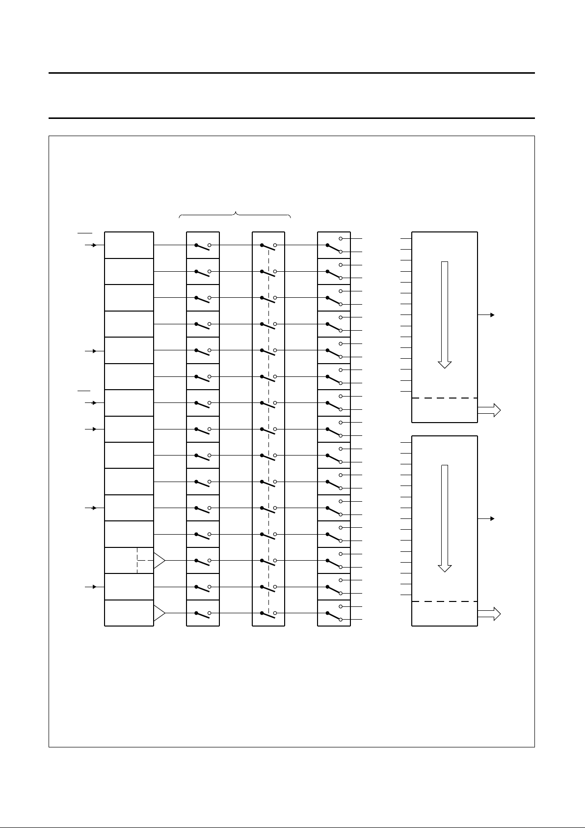
1996 Jun 27 64
Philips Semiconductors Product specification
8-bit microcontroller with on-chip CAN P8xC592
Fig.21 Interrupt system.
handbook, full pagewidth
interrupt
sources
source enable global enable
interrupt enable registers
a1
a2
b1
b2
c1
c2
d1
d2
e1
e2
f1
f2
g1
g2
h1
h2
i1
i2
j1
j2
k1
k2
l1
l2
m1
m2
n1
n2
o1
o2
interrupt priority
registers
a1
SOURCE
IDENTIFICATION
vector
b1
c1
d1
e1
f1
g1
h1
i1
j1
k1
l1
m1
n1
o1
high
priority
interrupt
request
MGA166
a2
SOURCE
IDENTIFICATION
vector
b2
c2
d2
e2
f2
g2
h2
i2
j2
k2
l2
m2
n2
o2
low
priority
interrupt
request
polling hardware
CT3I
CT2I
CT1I
CT0I
INT0
INT1
EXTERNAL
INTERRUPT
REQUEST 0
CAN
SERIAL
PORT 1
ADC
TIMER 0
OVERFLOW
TIMER 2
CAPTURE 0
TIMER 2
COMPARE 0
EXTERNAL
INTERRUPT
REQUEST 1
TIMER 2
CAPTURE 1
TIMER 2
COMPARE 1
TIMER 1
OVERFLOW
TIMER 2
CAPTURE 2
TIMER 2
COMPARE 2
UART
SERIAL
PORT 0
TIMER 2
CAPTURE 3
TIMER T2
OVERFLOW
T
R
Page 65

1996 Jun 27 65
Philips Semiconductors Product specification
8-bit microcontroller with on-chip CAN P8xC592
14.1 Interrupt Enable and Priority Registers
14.1.1 I
NTERRUPT ENABLE REGISTER 0 (IEN0)
Table 71 Interrupt Enable register 0 (address A8H)
Table 72 Description of the IEN0 bits
14.1.2 I
NTERRUPT ENABLE REGISTER 1 (IEN1)
Table 73 Interrupt Enable register 0 (address E8H)
Table 74 Description of the IEN1 bits
Logic 0 = interrupt disabled; Logic 1 = interrupt enabled.
76543210
EA EAD ES1 ES0 ET1 EX1 ET0 EX0
BIT SYMBOL FUNCTION
7EA General enable/disable control. If bit EA is:
LOW, then no interrupt is enabled.
HIGH, then any individually enabled interrupt will be accepted.
6 EAD Enable ADC interrupt.
5 ES1 Enable SIO1 (CAN) interrupt.
4 ES0 Enable SIO0 (UART) interrupt.
3 ET1 Enable Timer 1 interrupt.
2 EX1 Enable External 1 interrupt.
1 ET0 Enable Timer 0 interrupt.
0 EX0 Enable External 0 interrupt.
76543210
ET2 ECM2 ECM1 ECM0 ECT3 ECT2 ECT1 ECT0
BIT SYMBOL FUNCTION
7 ET2 Enable T2 overflow interrupt(s).
6 ECM2 Enable T2 comparator 2 interrupt.
5 ECM1 Enable T2 comparator 1 interrupt.
4 ECM0 Enable T2 comparator 0 interrupt.
3 ECT3 Enable T2 capture register 3 interrupt.
2 ECT1 Enable T2 capture register 2 interrupt.
1 ECT1 Enable T2 capture register 1 interrupt.
0 ECT0 Enable T2 capture register 0 interrupt.
Page 66

1996 Jun 27 66
Philips Semiconductors Product specification
8-bit microcontroller with on-chip CAN P8xC592
14.1.3 INTERRUPT PRIORITY REGISTER 0 (IP0)
Table 75 Interrupt Priority register 0 (address B8H)
Table 76 Description of the IP0 bits
14.1.4 I
NTERRUPT PRIORITY REGISTER 1 (IP1)
Table 77 Interrupt Priority register 1 (address F8H)
Table 78 Description of the IP1 bits
Logic 0 = low priority; Logic 1 = high priority.
76543210
−PAD PS1 PS0 PT1 PX1 PT0 PX0
BIT SYMBOL FUNCTION
7 − Not used.
6 PAD ADC interrupt priority level.
5 PS1 SIO1 (CAN) interrupt priority level.
4 PS0 SIO0 (UART) interrupt priority level.
3 PT1 Timer 1 interrupt priority level.
2 PX1 External interrupt 1 priority level.
1 PT0 Timer 0 interrupt priority level.
0 PX0 External interrupt 0 priority level.
76543210
PT2 PCM2 PCM1 PCM0 PCT3 PCT2 PCT1 PCT0
BIT SYMBOL FUNCTION
7 PT2 T2 overflow interrupt(s) priority level.
6 PCM2 T2 comparator 2 priority interrupt level.
5 PCM1 T2 comparator 1 priority interrupt level.
4 PCM0 T2 comparator 0 priority interrupt level.
3 PCT3 T2 capture register 3 priority interrupt level.
2 PCT2 T2 capture register 2 priority interrupt level.
1 PCT1 T2 capture register 1 priority interrupt level.
0 PCT0 T2 capture register 0 priority interrupt level.
Page 67

1996 Jun 27 67
Philips Semiconductors Product specification
8-bit microcontroller with on-chip CAN P8xC592
14.2 Interrupt Vectors
The vector indicates the Program Memory location where
the appropriate interrupt service routine starts
(see Table 79).
Table 79 Interrupt vectors
SOURCE BIT VECTOR
External 0 X0 0003H
Timer 0 overflow T0 000BH
External 1 X1 0013H
Timer 1 overflow T1 001BH
Serial I/O 0 (UART) S0 0023H
Serial I/O 1 (CAN) S1 002BH
T2 capture 0 CT0 0033H
T2 capture 1 CT1 003BH
T2 capture 2 CT2 0043H
T2 capture 3 CT3 004BH
ADC completion ADC 0053H
T2 compare 0 CM0 005BH
T2 compare 1 CM1 0063H
T2 compare 2 CM2 006BH
T2 overflow T2 0073H
14.3 Interrupt Priority
Each interrupt source can be either high priority or low
priority. If both priorities are requested simultaneously, the
processor will branch to the high priority vector. If there are
simultaneous requests from sources of the same priority,
then interrupts will be serviced in the following order:
X0, S1, ADC, T0, CT0, CM0, X1, CT1, CM1, T1, CT2,
CM2, S0, CT3, T2.
A low priority interrupt routine can only be interrupted by a
high priority interrupt. A high priority interrupt routine can
not be interrupted.
15 POWER REDUCTION MODES
The P8xC592 has three software-selectable modes to
reduce power consumption. These are:
• Sleep mode, affecting the CAN-controller only
• Idle mode, affecting the
– CPU (halted)
– Timer 2 (stopped and reset)
– PWM0, PWM1 (reset, output = HIGH)
– ADC (aborted if in progress)
• Power-down mode, affecting the whole P8xC592
device.
handbook, full pagewidth
MGA167
OSCILLATOR
CLOCK
GENERATOR
interrupts
serial ports
timer blocks
CPU
T2
PWM
ADC
IDL
PD
XTAL1XTAL2
CAN
sleep
Fig.22 Internal Sleep, Idle and Power-down clock configuration.
Page 68

1996 Jun 27 68
Philips Semiconductors Product specification
8-bit microcontroller with on-chip CAN P8xC592
15.1 Power Control Register (PCON)
Table 80 Power Control Register (address 87H)
Table 81 Description of the PCON bits
Note
1. If PD and IDL are set to HIGH at the same time, PD takes precedence. The reset value of PCON is 0XX00000B.
76543210
SMOD −−WLE GF1 GF0 PD IDL
BIT SYMBOL FUNCTION
7 SMOD Double baud rate bit. When set to logic 1 the baud rate is doubled when the serial port
SIO0 is being used in Modes 1, 2 and 3.
6 − Reserved.
5 −
4 WLE Watchdog Load Enable. This flag must be set by software prior to loading T3
(Watchdog timer). It is cleared when T3 is loaded.
3 GF1 General purpose flag bits.
2 GF0
1PD Power-down bit. Setting this bit activates Power-down mode (note 1). It can only be set
if input
EW is HIGH.
0 IDL Idle mode bit. Setting this bit activates the Idle mode (note 1).
15.2 CAN Sleep Mode
In order to reduce power consumption of the P8xC592 the
CAN-controller may be switched off (disconnecting the
internal clock) by setting the CAN Command Register bit 4
(Sleep) HIGH. The CAN-controller leaves this Sleep mode
by detecting either activity on the CAN-bus (dominant
bit-level on CRX0/CRX1; see Chapter 5, Table 1) or by
setting the Sleep bit to LOW. As the CPU can not only write
to the Sleep bit, but can also read it, the CAN-controller
status can be determined directly.
15.3 Idle Mode
The instruction that sets bit PCON.0 to HIGH is the last
one executed in the normal operating mode before Idle
mode is activated.
Once in the Idle mode, the CPU status is preserved in its
entirety: the Stack Pointer, Program Counter, Program
Status Word, Accumulator, RAM and all other registers
maintain their data during Idle mode. The status of the
external pins during Idle mode is shown in see Table 82.
There are three ways to terminate the Idle mode:
• Activation of any enabled interrupt will cause PCON.0 to
be cleared by hardware, provided that the interrupt
source is active during Idle mode. After the interrupt is
serviced, the program continues with the instruction
immediately after the one, at which the interrupt request
was detected.
• The flag bits GF0 and GF1 may be used to determine
whether the interrupt was received during normal
execution or during the Idle mode. For example, the
instruction that writes to PCON.0 can also set or clear
one or both flag bits. When Idle mode is terminated by
an interrupt, the service routine can examine the status
of the flag bits.
• Another way of terminating the Idle mode is an external
hardware reset. Since the oscillator is still running, the
reset signal is required to be active only for two machine
cycles (24 oscillator periods) to complete the reset
operation.
• The third way is the internally generated watchdog reset
after an overflow of Timer 3.
Page 69

1996 Jun 27 69
Philips Semiconductors Product specification
8-bit microcontroller with on-chip CAN P8xC592
15.4 Power-down Mode
The instruction that sets bit PCON.1 to HIGH, is the last
one executed before entering the Power-down mode. In
Power-down mode the oscillator of the P8xC592 is
stopped. If the CAN-controller is in use, it is recommended
to set it into Sleep mode before entering Power-down
mode. However, setting PCON.1 to HIGH also sets the
Sleep bit (CAN-controller Command Register bit 4) to
HIGH.
The P8xC592 leaves Power-down mode either by a
hardware reset or by a CAN Wake-Up interrupt
(due to activity on the CAN-bus),
if the SIO1 (CAN) interrupt source is enabled
(contents of register IEN0 = 1X1XXXXXB).
A hardware reset affects the whole P8xC592, but leaves
the contents of the on-chip RAM unchanged
(CAN-controller-and CPU's SFRs are reset, see
Section 13.5.2, Chapter 17 and Table 40). A CAN
Wake-Up interrupt during Power-down mode causes a
reset output pulse with a width of 6144 machine cycles
(4.6 ms with f
CLK
= 16 MHz). All hardware except that for
the CAN-controller of the P8xC592 is reset (i.e. the
contents of all CAN-controller registers are preserved).
A capacitance connected to the RST pin can be used to
lengthen the internally generated reset pulse. If the pulse
exceeds 8192 machine cycles, the CAN-controller part is
reset too.
Table 82 Status of external pins during Idle and Power-down modes
Note
1. If the port pins P1.6 and P1.7 are used as the CAN transmitter outputs (CTX0 and CTX1), then during Sleep and
Power-down mode these pins output a ‘recessive’ level (see Sections 13.5.2 and 13.5.11).
MODE PROGRAM ALE
PSEN PORT0 PORT1
(1)
PORT2 PORT3 PORT4
PWM0/
PWM1
Idle internal 1 1 port data port data port data port data port data 1
external 1 1 floating port data address port data port data 1
Power-down internal 0 0 port data port data port data port data port data 1
external 0 0 floating port data port data port data port data 1
Page 70
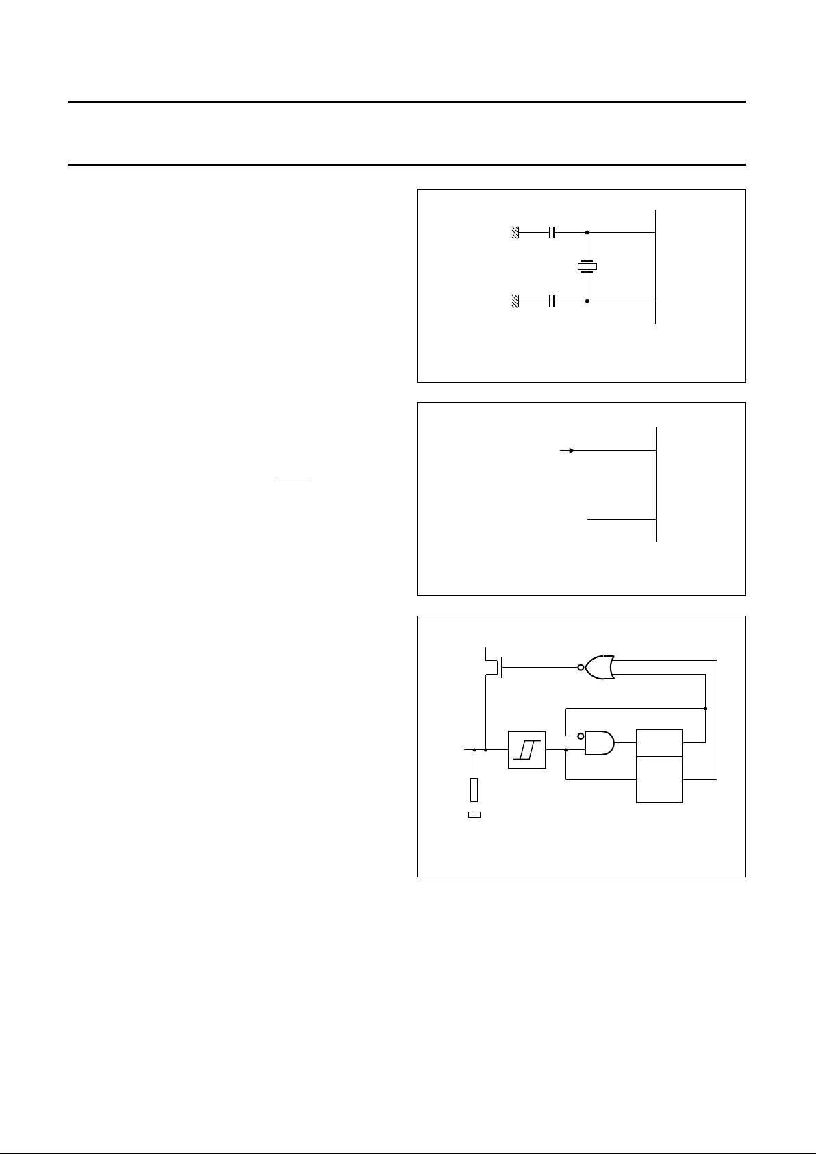
1996 Jun 27 70
Philips Semiconductors Product specification
8-bit microcontroller with on-chip CAN P8xC592
16 OSCILLATOR CIRCUITRY
The oscillator circuitry of the P8xC592 is a single-stage
inverting amplifier in a Pierce oscillator configuration. The
circuitry between XTAL1 and XTAL2 is basically an
inverter biased to the transfer point. Either a crystal or
ceramic resonator can be used as the feedback element to
complete the oscillator circuitry. Both are operated in
parallel resonance. XTAL1 (pin 34) is the high gain
amplifier input, and XTAL2 (pin 33) is the output
(see Fig.23). If XTAL1 is driven from an external source,
XTAL2 must be left open (see Fig.24).
Fig.23 P8xC592 oscillator circuit.
handbook, halfpage
C1
XTAL1
XTAL2
20 pF
C2
MLA888
20 pF
34
33
Fig.24 Driving P8xC592 from an external source.
handbook, halfpage
XTAL1
XTAL2
MLA889
external clock
(not TTL compatible)
not connected
34
33
17 RESET CIRCUITRY
The reset pin RST is connected to a Schmitt trigger for
noise rejection (see Fig.25). A reset is accomplished by
holding the RST pin HIGH for at least two machine cycles
(24 oscillator periods). The CPU responds by executing an
internal reset. During reset ALE and PSEN output a HIGH
level. In order to perform a correct reset, this level must not
be affected by external elements.
Also with the P8xC592, the RST line can be pulled HIGH
internally by a pull-up transistor activated by the Watchdog
timer T3. The length of the output pulse from T3 is
3 machine cycles. A pulse of such short duration is
necessary in order to recover from a processor or system
fault as fast as possible.
During Power-down a reset could be generated internally
via the CAN Wake-Up interrupt. Then the RST pin is pulled
HIGH for 6144 machine cycles. In this case the
CAN-controller is not reset.
If the Watchdog timer or the CAN Wake-Up interrupt is
used to reset external devices, the usual capacitor
arrangement for Power-on-reset (see Fig.26) should not
be used.
However, the internal reset is forced, independent of the
external level on the RST pin.
The MAIN RAM and AUXILIARY RAM are not affected.
When VDD is turned on, the RAM content is indeterminate.
A reset leaves the internal registers as shown in Table 83.
handbook, halfpage
MGA170 - 1
overflow timer T3
V
DD
RST
on-chip
RST
R
wake-up reset
CAN
CPU
Fig.25 On-chip reset configuration.
Page 71

1996 Jun 27 71
Philips Semiconductors Product specification
8-bit microcontroller with on-chip CAN P8xC592
Table 83 Internal registers' contents after a reset
X = undefined state.
REGISTER 7 6 5 4 3 2 1 0
CPU part
ACC 00000000
ADC0 X X 0 0 0 0 0 0
ADCH X X X X X X X X
B 00000000
CML0 to CML2 0 0 0 0 0 0 0 0
CMH0 to CMH2 0 0 0 0 0 0 0 0
CTCON 0 0 0 0 0 0 0 0
CTL0 to CTL3 X X X X X X X X
CTH0 to CTH3 X X X X X X X X
DPL 00000000
DPH 00000000
IEN0 0 0 0 0 0 0 0 0
IEN1 0 0 0 0 0 0 0 0
IP0 X0000000
IP1 00000000
PCH 00000000
PCL 00000000
PCON 0 X X 0 0 0 0 0
PSW 00000000
PWM0 0 0 0 0 0 0 0 0
PCWM1 0 0 0 0 0 0 0 0
PCWMP 0 0 0 0 0 0 0 0
P0toP4 11111111
P5 XXXXXXXX
RTE 00000000
S0BUF X X X X X X X X
S0CON 0 0 0 0 0 0 0 0
CANSTA 0 0 0 0 1 1 0 0
CANCON X X X 0 0 0 0 0
CANDAT X X X X X X X X
CANADR 0 X 1 0 0 1 0 0
SP 00000111
STE 11000000
TCON 0 0 0 0 0 0 0 0
TH0, TH1 0 0 0 0 0 0 0 0
TMH2 0 0 0 0 0 0 0 0
TL0, TL1 0 0 0 0 0 0 0 0
TML2 0 0 0 0 0 0 0 0
TMOD 0 0 0 0 0 0 0 0
TM2CON 0 0 0 0 0 0 0 0
TM2IR 0 0 0 0 0 0 0 0
T3 00000000
CAN part
CR 0X1XXXX1
CMR 11X0XXXX
SR 00001100
IR XXX00000
ACR XXXXXXXX
AMR XXXXXXXX
BTR0 X X X X X X X X
BTR1 X X X X X X X X
OCR XXXXXXXX
TR XXXXXXXX
TXB 10 to 19 X X X X X X X X
RXB 20 to 29 X X X X X X X X
REGISTER 7 6 5 4 3 2 1 0
Page 72

1996 Jun 27 72
Philips Semiconductors Product specification
8-bit microcontroller with on-chip CAN P8xC592
17.1 Power-on Reset
If the RST pin is connected to VDD via a 2.2 µF capacitor,
as shown in Fig.26, an automatic reset can be obtained by
switching on VDD (provided its rise time is <10 ms). The
decrease of the RST pin voltage depends on the capacitor
and the internal resistor R
RST
. That voltage must remain
above the lower threshold for at minimum the oscillator
start-up time plus 2 machine cycles.
18 INSTRUCTION SET
The P8xC592 uses the powerful instruction set of the
P80C51. It consists of 49 single-byte, 45 two-byte and
17 three-byte instructions. Using a 16 MHz quartz, 64 of
the instructions are executed in 0.75 µs, 45 in 1.5 µs and
the multiply, divide instructions in 3 µs. A summary of the
instruction set is given in Tables 84, 85, 86, 87 and 88.
Fig.26 Power-on-reset.
dbook, halfpage
V
DD
V
DD
RST
2.2 µF
R
RST
MGA171
P8xC592
18.1 Addressing Modes
Most instructions have a ‘destination/source’ field that
specifies the data type, addressing modes and operands
involved. For all these instructions, except from MOVs, the
destination operand is also a source operand
(e.g. ADD A, R7).
Five types of addressing modes are used:
• Register Addressing,
– R0 to R7 (4 banks)
– A,B,C (bit), AB (2 bytes), DPTR (double byte).
• Direct Addressing,
– lower 128 bytes of internal MAIN RAM
(including the 4 R0 to R7 register banks)
– Special Function Registers (SFRs)
– 128 bits in a subset of the internal MAIN RAM
(see Fig.5)
– 128 bits in a subset of the Special Function Registers
(see Figs 6 and 7).
• Register-Indirect Addressing,
– internal RAM (@R0, @R1, @SP [PUSH/POP])
– internal AUXILIARY RAM (@R0, @R1, @DPTR)
– external Data Memory (@DPTR).
• Immediate Addressing,
– Program Memory (in-code 8 bit or 16 bit constant).
• Base-Register-plus Index-Register-Indirect Addressing,
– Program Memory look-up table
(@DPTR+A, @PC+A).
The first three addressing modes are usable for
destination operands.
Page 73

1996 Jun 27 73
Philips Semiconductors Product specification
8-bit microcontroller with on-chip CAN P8xC592
18.2 Instruction Set
For the description of the Data Addressing Modes and Hexadecimal opcode cross-reference see Table 88.
Table 84 Instruction set description: Arithmetic operations
MNEMONIC DESCRIPTION BYTES CYCLES
OPCODE
(HEX)
Arithmetic operations
ADD A,Rr Add register to A 1 1 2*
ADD A,direct Add direct byte to A 2 1 25
ADD A,@Ri Add indirect RAM to A 1 1 26, 27
ADD A,#data Add immediate data to A 2 1 24
ADDC A,Rr Add register to A with carry flag 1 1 3*
ADDC A,direct Add direct byte to A with carry flag 2 1 35
ADDC A,@Ri Add indirect RAM to A with carry flag 1 1 36, 37
ADDC A,#data Add immediate data to A with carry flag 2 1 34
SUBB A,Rr Subtract register from A with borrow 1 1 9*
SUBB A,direct Subtract direct byte from A with borrow 2 1 95
SUBB A,@Ri Subtract indirect RAM from A with borrow 1 1 96, 97
SUBB A,#data Subtract immediate data from A with borrow 2 1 94
INC A Increment A 1 1 04
INC Rr Increment register 1 1 0*
INC direct Increment direct byte 2 1 05
INC @Ri Increment indirect RAM 1 1 06, 07
DEC A Decrement A 1 1 14
DEC Rr Decrement register 1 1 1*
DEC direct Decrement direct byte 2 1 15
DEC @Ri Decrement indirect RAM 1 1 16, 17
INC DPTR Increment data pointer 1 2 A3
MUL AB Multiply A and B 1 4 A4
DIV AB Divide A by B 1 4 84
DA A Decimal adjust A 1 1 D4
Page 74

1996 Jun 27 74
Philips Semiconductors Product specification
8-bit microcontroller with on-chip CAN P8xC592
Table 85 Instruction set description: Logic operations
MNEMONIC DESCRIPTION BYTES CYCLES
OPCODE
(HEX)
Logic operations
ANL A,Rr AND register to A 1 1 5*
ANL A,direct AND direct byte to A 2 1 55
ANL A,@Ri AND indirect RAM to A 1 1 56, 57
ANL A,#data AND immediate data to A 2 1 54
ANL direct,A AND A to direct byte 2 1 52
ANL direct,#data AND immediate data to direct byte 3 2 53
ORL A,Rr OR register to A 1 1 4*
ORL A,direct OR direct byte to A 2 1 45
ORL A,@Ri OR indirect RAM to A 1 1 46, 47
ORL A,#data OR immediate data to A 2 1 44
ORL direct,A OR A to direct byte 2 1 42
ORL direct,#data OR immediate data to direct byte 3 2 43
XRL A,Rr Exclusive-OR register to A 1 1 6*
XRL A,direct Exclusive-OR direct byte to A 2 1 65
XRL A,@Ri Exclusive-OR indirect RAM to A 1 1 66, 67
XRL A,#data Exclusive-OR immediate data to A 2 1 64
XRL direct,A Exclusive-OR A to direct byte 2 1 62
XRL direct,#data Exclusive-OR immediate data to direct byte 3 2 63
CLR A Clear A 1 1 E4
CPL A Complement A 1 1 F4
RL A Rotate A left 1 1 23
RLC A Rotate A left through the carry flag 1 1 33
RR A Rotate A right 1 1 03
RRC A Rotate A right through the carry flag 1 1 13
SWAP A Swap nibbles within A 1 1 C4
Page 75

1996 Jun 27 75
Philips Semiconductors Product specification
8-bit microcontroller with on-chip CAN P8xC592
Table 86 Instruction set description: Data transfer
Note
1. MOV A,ACC is not permitted.
MNEMONIC DESCRIPTION BYTES CYCLES
OPCODE
(HEX)
Data transfer
MOV A,Rr Move register to A 1 1 E*
MOV A,direct (note 1) Move direct byte to A 2 1 E5
MOV A,@Ri Move indirect RAM to A 1 1 E6, E7
MOV A,#data Move immediate data to A 2 1 74
MOV Rr,A Move A to register 1 1 F*
MOV Rr,direct Move direct byte to register 2 2 A*
MOV Rr,#data Move immediate data to register 2 1 7*
MOV direct,A Move A to direct byte 2 1 F5
MOV direct,Rr Move register to direct byte 2 2 8*
MOV direct,direct Move direct byte to direct 3 2 85
MOV direct,@Ri Move indirect RAM to direct byte 2 2 86, 87
MOV direct,#data Move immediate data to direct byte 3 2 75
MOV @Ri,A Move A to indirect RAM 1 1 F6, F7
MOV @Ri,direct Move direct byte to indirect RAM 2 2 A6, A7
MOV @Ri,#data Move immediate data to indirect RAM 2 1 76, 77
MOV DPTR,#data16 Load data pointer with a 16-bit constant 3 2 90
MOVC A,@A+DPTR Move code byte relative to DPTR to A 1 2 93
MOVC A,@A+PC Move code byte relative to PC to A 1 2 83
MOVX A,@Ri Move external RAM (8-bit address) to A 1 2 E2, E3
MOVX A,@DPTR Move external RAM (16-bit address) to A 1 2 E0
MOVX @Ri,A Move A to external RAM (8-bit address) 1 2 F2, F3
MOVX @DPTR,A Move A to external RAM (16-bit address) 1 2 F0
PUSH direct Push direct byte onto stack 2 2 C0
POP direct Pop direct byte from stack 2 2 D0
XCH A,Rr Exchange register with A 1 1 C*
XCH A,direct Exchange direct byte with A 2 1 C5
XCH A,@Ri Exchange indirect RAM with A 1 1 C6, C7
XCHD A,@Ri Exchange LOW-order digit indirect RAM with A 1 1 D6, D7
Page 76

1996 Jun 27 76
Philips Semiconductors Product specification
8-bit microcontroller with on-chip CAN P8xC592
Table 87 Instruction set description: Boolean variable manipulation, Program and machine control
MNEMONIC DESCRIPTION BYTES CYCLES
OPCODE
(HEX)
Boolean variable manipulation
CLR C Clear carry flag 1 1 C3
CLR bit Clear direct bit 2 1 C2
SETB C Set carry flag 1 1 D3
SETB bit Set direct bit 2 1 D2
CPL C Complement carry flag 1 1 B3
CPL bit Complement direct bit 2 1 B2
ANL C,bit AND direct bit to carry flag 2 2 82
ANL C,/bit AND complement of direct bit to carry flag 2 2 B0
ORL C,bit OR direct bit to carry flag 2 2 72
ORL C,/bit OR complement of direct bit to carry flag 2 2 A0
MOV C,bit Move direct bit to carry flag 2 1 A2
MOV bit,C Move carry flag to direct bit 2 2 92
Program and machine control
ACALL addr11 Absolute subroutine call 2 2 •1
LCALL addr16 Long subroutine call 3 2 12
RET Return from subroutine 1 2 22
RETI Return from interrupt 1 2 32
AJMP addr11 Absolute jump 2 2 ♦1
LJMP addr16 Long jump 3 2 02
SJMP rel Short jump (relative address) 2 2 80
JMP @A+DPTR Jump indirect relative to the DPTR 1 2 73
JZ rel Jump if A is zero 2 2 60
JNZ rel Jump if A is not zero 2 2 70
JC rel Jump if carry flag is set 2 2 40
JNC rel Jump if carry flag is not set 2 2 50
JB bit,rel Jump if direct bit is set 3 2 20
JNB bit,rel Jump if direct bit is not set 3 2 30
JBC bit,rel Jump if direct bit is set and clear bit 3 2 10
CJNE A,direct,rel Compare direct to A and jump if not equal 3 2 B5
CJNE A,#data,rel Compare immediate to A and jump if not equal 3 2 B4
CJNE Rr,#data,rel Compare immediate to register and jump if not equal 3 2 B*
CJNE @Ri,#data,rel Compare immediate to indirect and jump if not equal 3 2 B6, B7
DJNZ Rr,rel Decrement register and jump if not zero 2 2 D*
DJNZ direct,rel Decrement direct and jump if not zero 3 2 D5
NOP No operation 1 1 00
Page 77

1996 Jun 27 77
Philips Semiconductors Product specification
8-bit microcontroller with on-chip CAN P8xC592
Table 88 Description of the mnemonics in the Instruction set
MNEMONIC DESCRIPTION
Data addressing modes
Rr Working register R0-R7.
direct 128 internal RAM locations and any special function register (SFR).
@Ri Indirect internal RAM location addressed by register R0 or R1 of the actual register bank.
#data 8-bit constant included in instruction.
#data 16 16-bit constant included as bytes 2 and 3 of instruction.
bit Direct addressed bit in internal RAM or SFR.
addr16 16-bit destination address. Used by LCALL and LJMP.
The branch will be anywhere within the 64 kbytes Program Memory address space.
addr11 11-bit destination address. Used by ACALL and AJMP. The branch will be within the same 2 kbytes
page of Program Memory as the first byte of the following instruction.
rel Signed (two's complement) 8-bit offset byte. Used by SJMP and all conditional jumps.
Range is −128 to +127 bytes relative to first byte of the following instruction.
Hexadecimal opcode cross-reference
* 8, 9, A, B, C, D, E, F.
• 1, 3, 5, 7, 9, B, D, F.
♦ 0, 2, 4, 6, 8, A, C, E.
Page 78

1996 Jun 27 78
Philips Semiconductors Product specification
8-bit microcontroller with on-chip CAN P8xC592
Table 89 Instruction map
Note
1. MOV A, ACC is not a valid instruction.
First hexadecimal character of opcode ← Second hexadecimal character of opcode →
↓ 0123 456789ABCDEF
0 NOP
AJMP
addr11
LJMP
addr16
RR
A
INC
A
INC
direct
INC @Ri INC Rr
0 1 01234567
1
JBC
bit,rel
ACALL
addr11
LCALL
addr16
RRC
A
DEC
A
DEC
direct
DEC @Ri DEC Rr
0 1 01234567
2
JB
bit,rel
AJMP
addr11
RET
RL
A
ADD
A,#data
ADD
A,direct
ADD A,@Ri ADD A,Rr
0 1 01234567
3
JNB
bit,rel
ACALL
addr11
RETI
RLC
A
ADDC
A,#data
ADDC
A,direct
ADDC A,@Ri ADDC A,Rr
0 1 01234567
4
JC
rel
AJMP
addr11
ORL
direct,A
ORL
direct,#data
ORL
A,#data
ORL
A,direct
ORL A,@Ri ORL A,Rr
0 1 01234567
5
JNC
rel
ACALL
addr11
ANL
direct,A
ANL
direct,#data
ANL
A,#data
ANL
A,direct
ANL A,@Ri ANL A,Rr
0 1 01234567
6
JZ
rel
AJMP
addr11
XRL
direct,A
XRL
direct,#data
XRL
A,#data
XRL
A,direct
XRL A,@Ri XRL A,Rr
0 1 01234567
7
JNZ
rel
ACALL
addr11
ORL
C,bit
JMP
@A+DPTR
MOV
A,#data
MOV
direct,#data
MOV @Ri,#data MOV Rr,#data
0 1 01234567
8
SJMP
rel
AJMP
addr11
ANL
C,bit
MOVC
A,@A+PC
DIV
AB
MOV
direct,direct
MOV direct,@Ri MOV direct,Rr
0 1 01234567
9
MOV
DTPR,#data16
ACALL
addr11
MOV
bit,C
MOVC
A,@A+DPTR
SUBB
A,#data
SUBB
A,direct
SUBB A,@Ri SUB A,Rr
0 1 01234567
A
ORL
C,/bit
AJMP
addr11
MOV
bit,C
INC
DPTR
MUL
AB
MOV @Ri,direct MOV Rr,direct
0 1 01234567
B
ANL
C,/bit
ACALL
addr11
CPL
bit
CPL
C
CJNE
A,#data,rel
CJNE
A,direct,rel
CJNE @Ri,#data,rel CJNE Rr,#data,rel
0 1 01234567
C
PUSH
direct
AJMP
addr11
CLR
bit
CLR
C
SWAP
A
XCH
A,direct
XCH A,@Ri XCH A,Rr
0 1 01234567
D
POP
direct
ACALL
addr11
SETB
bit
SETB
C
DA
A
DJNZ
direct,rel
XCHD A,@Ri DJNZ Rr,rel
0 1 01234567
E
MOVX
A,@DTPR
AJMP
addr11
MOVX A,@Ri
CLR
A
MOV
A,direct
(1)
MOV A,@Ri MOV A,Rr
0 1 0 1 01234567
F
MOVX
@DTPR,A
ACALL
addr11
MOVX @Ri,A
CPL
A
MOV
direct,A
MOV @Ri,A MOV Rr,A
0 1 0 1 01234567
Page 79

1996 Jun 27 79
Philips Semiconductors Product specification
8-bit microcontroller with on-chip CAN P8xC592
19 ABSOLUTE MAXIMUM RATINGS (note 1)
In accordance with the Absolute Maximum Rating System (IEC 134).
Notes
1. The following applies to the Absolute Maximum Ratings:
a) Stresses above those listed under Absolute Maximum Ratings may cause permanent damage to the device.
This is a stress rating only and functional operation of the device at these or any conditions other than those
described in the Chapters 20 “DC characteristics” and 21 “AC characteristics” of this specification is not implied.
b) This product includes circuitry specifically designed for the protection of its internal devices from the damaging
effect of excessive static charge. However, it is suggested that conventional precautions be taken to avoid
applying greater than the rated maxima.
c) Parameters are valid over operating temperature range unless otherwise specified.
All voltages are with respect to V
SS
unless otherwise noted.
2. This value is based on the maximum allowable die temperature and the thermal resistance of the package, not on
device power consumption.
SYMBOL PARAMETER MIN. MAX. UNIT
V
DD
voltage on VDD pin −0.5 +6.5 V
V
I1
input voltage on any pin
(except CTX0, CTX1, CRX0, CRX1 and EA/VPP)
−0.5 VDD+ 0.5 V
V
I2
input voltage on EA/VPP to V
SS
−0.5 +13 V
I
I
, I
O
input/output current on any single I/O pin
(except from CTX0 and CTX1)
−±10 mA
I
OT
sink current of CTX0, CTX1 together − 30 mA
source current of CTX0, CTX1 together −−20 mA
P
tot
total power dissipation (note 2) − 1.0 W
T
stg
storage temperature range −65 +150 °C
T
amb
operating ambient temperature range:
P8xC592 FFA −40 +85 °C
P8xC592 FHA −40 +125 °C
Page 80

1996 Jun 27 80
Philips Semiconductors Product specification
8-bit microcontroller with on-chip CAN P8xC592
20 DC CHARACTERISTICS
VDD=5V±10%; VSS= 0 V; all voltages with respect to VSS unless otherwise specified.
T
amb
= −40 to +125 °C for the P8xC592FHA; T
amb
= −40 to +85 °C for the P8xC592FFA.
SYMBOL PARAMETER CONDITIONS MIN. MAX. UNIT
Supply (digital part)
V
DD
supply voltage 4.5 5.5 V
I
DD
operating supply current f
CLK
= 16 MHz; note 1 − 50 mA
I
DD(ID)
supply current Idle mode f
CLK
= 16 MHz; note 2 − 15 mA
I
DD(IS)
supply current Idle & Sleep mode f
CLK
= 16 MHz; note 3 − 10 mA
I
DD(PD)
supply current Power-down mode: note 4
P8xC592 FHA − 150 µA
P8xC592 xFx − 50 µA
Inputs
V
IL
LOW level input voltage
(except EA, CRX0 and CRX1)
−0.5 0.2VDD− 0.1 V
V
IL1
LOW level input voltage EA −0.5 0.2VDD− 0.3 V
V
IH
HIGH level input voltage
(except RST, XTAL1, CRX0,CRX1)
0.2VDD+ 0.9 VDD+ 0.5 V
V
IH1
HIGH level input voltage
(RST and XTAL1)
0.7V
DD
VDD+ 0.5 V
I
IL
LOW level input current
Ports 1, 2, 3 and 4
VI= 0.45 V −−50 µA
I
TL
input current HIGH-to-LOW
transition
Ports 1, 2, 3 and 4
(except P1.6 and P1.7)
VI= 2.0 to 0.45 V −−650 µA
I
LI1
input leakage current
Port 0, EA, STADC, EW, P1.6, P1.7
0.45 V < VI< V
DD
−±10 µA
I
LI2
input leakage current Port 5 0.45 V < VI< V
DD
−±1µA
Outputs
V
OL
LOW level output voltage
Ports 1, 2, 3 and 4
(except P1.6 and P1.7)
IOL= 1.6 mA; note 5 − 0.45 V
V
OL1
LOW level output voltage
Port 0, ALE, PSEN, PWM0, PWM1,
P1.6, P1.7
IOL= 3.2 mA; note 5 − 0.45 V
V
OH
HIGH level output voltage
Ports 1, 2, 3 and 4
(except P1.6 and P1.7)
IOH= −60 µA 2.4 − V
I
OH
= −25 µA 0.75V
DD
− V
I
OH
= −10 µA 0.9V
DD
− V
V
OH1
HIGH level output voltage
Port 0 in external bus mode,
ALE, PSEN, PWM0, PWM1
IOH= −400 µA 2.4 − V
I
OH
= −150 µA 0.75V
DD
− V
I
OH
= −40 µA; note 6 0.9V
DD
− V
Page 81

1996 Jun 27 81
Philips Semiconductors Product specification
8-bit microcontroller with on-chip CAN P8xC592
V
OH2
HIGH level output voltage RST IOH= −400 µA 2.4 − V
I
OH
= −120 µA 0.8V
DD
− V
R
RST
RST pull-down resistor 50 150 kΩ
C
I/O
I/O pin capacitance test frequency = 1 MHz;
T
amb
=25°C
− 10 pF
Supply (analog part)
AV
DD
supply voltage AVDD=VDD± 0.2 V 4.5 5.5 V
AI
DD
operating supply current Port 5 = AVDD; note 1 − 2.5 mA
AI
DD(ID)
supply current Idle mode note 2 − 2.5 mA
AI
DD(IS)
supply current Idle and Sleep mode: note 3
P83C592 FHA − 400 µA
P8xC592 xFx − 350 µA
AI
DD(PD)
supply current Power-down mode: note 4
P83C592 FHA − 400 µA
P8xC592 xFx − 350 µA
Analog inputs
AV
IN
analog input voltage AVSS− 0.2 AVDD+ 0.2 V
AV
REF−
reference voltage AVSS− 0.2 − V
AV
REF+
− AVDD+ 0.2 V
R
REF
resistance between
AV
REF+
and AV
REF−
10 50 kΩ
C
IA
analog input capacitance − 15 pF
t
ADS
sampling time note 7 − 8t
CY
µs
t
ADC
conversion time
(including sample time)
note 7 − 50t
CY
µs
DL
e
differential non-linearity notes 8, 9 and 10 −±1 LSB
IL
e
integral non-linearity notes 8 and 11 −±2 LSB
OS
e
offset error notes 8 and 12 −±2 LSB
G
e
gain error notes 8 and 13 −±0.4 %
A
e
absolute voltage error notes 8 and 14 −±3 LSB
M
ctc
channel to channel matching −±1 LSB
C
t
crosstalk between P5 inputs 0 to 100 kHz −−60 dB
CAN input comparator (CRX0, CRX1)
V
DIF
differential input voltage (note 15) AVDD=5V±5%;
1.4 V < VI< AVDD−1.4 V
±32 − mV
V
HYST
hysteresis voltage (note 15) 8 30 mV
I
I
input current −±400 nA
SYMBOL PARAMETER CONDITIONS MIN. MAX. UNIT
Page 82

1996 Jun 27 82
Philips Semiconductors Product specification
8-bit microcontroller with on-chip CAN P8xC592
Notes to the DC characteristics
1. Conditions for:
a) The digital operating current measurement: all output pins disconnected; XTAL1 is driven with tr=tf= 10 ns;
VIL=VSS+ 0.5 V; VIH=VDD− 0.5 V; EA = RST = Port 0 = P1.6 = P1.7 = EW = VDD;
STADC = VSS; CRX0 = 2.7 V; CRX1 = 2.3 V.
b) The analog operating current measurement: Port 5 = AVDD; CAN: register 6: = 00H;
load current reference voltage source 100 µA.
2. Conditions for:
a) The digital Idle mode supply current measurement: all output pins disconnected;
XTAL1 is driven with tr=tf= 10 ns; VIL=VSS+ 0.5 V; VIH=VDD− 0.5 V; Port 0 = P1.6 = P1.7 = EW=VDD;
EA = RST = STADC = VSS; CRX0 = 2.7 V; CRX1 = 2.3 V.
b) The analog Idle mode current measurement: Port 5 = AVDD; CAN: register 6: = 00H;
load current reference voltage source 100 µA.
3. Conditions for:
a) The digital Idle and Sleep mode supply current measurement: all output pins disconnected;
XTAL1 is driven with tr=tf= 10 ns; VIL=VSS+ 0.5 V; VIH=VDD− 0.5 V;
Port 0 = P1.6 = P1.7 = EW = CRX0 = VDD; EA = RST = STADC = CRX1 = VSS;
CAN: register 6: = 00H, register 7: = 12H, register 8: = 02H, register 0: = 20H, wait 15tCY,
register 1: = 10H, wait for bit Sleep = 1.
b) The analog Idle and Sleep mode current measurement: Port5=AVDD;
load current reference voltage source 100 µA.
4. Window devices have to be covered. Conditions for:
a) The digital Power-down mode supply current measurement: all output pins and Port 5 disconnected;
Port 0 = P1.6 = P1.7 =
EW = CRX0 = VDD;
EA = RST = STADC = CRX1 = XTAL1 = AV
REF+
= AV
REF−
= CVSS=VSS;
AVDD=VDD, but current into AVDD pin is not comprised in digital Power-down current.
b) The analog Power-down mode supply current measurement: Port 5 = AVDD.
5. Capacitive loads on Port 0 and Port 2 may degrade the LOW level output voltage of ALE, Port 1 and Port 3.
During a HIGH-to-LOW transition on the Port 0 and Port 2 pins and a capacitive load >100 pF, the ALE LOW level
may exceed 0.8 V. In the case that it is necessary to connect ALE to a Schmitt trigger input respectively use an
address latch with a Schmitt trigger STROBE input.
CAN output driver (V
DD
=5V± 5%)
V
OLT
LOW level output voltage
(CTX0 and CTX1)
Io= 1.2 mA; note 15 − 0.1 V
I
o
=10mA − 0.6 V
V
OHT
High level output voltage
(CTX0 and CTX1)
Io= −1.2 mA; note 15 VDD− 0.1 − V
I
o
= −10 mA; note 16 VDD− 0.6 − V
Reference (AV
DD
=5V± 5%)
V
REFOUT
REF output voltage −0.1 mA < IL< 0.1 mA;
CL= 10 nF; note 15;
bit Reference Active = HIGH
1
⁄2AVDD−0.11⁄2AVDD+0.1 V
I
REFIN
REF input current 1.5 V < V
REFIN
< AVDD−1.5 V;
bit Reference Active = LOW
−±10 µA
SYMBOL PARAMETER CONDITIONS MIN. MAX. UNIT
Page 83

1996 Jun 27 83
Philips Semiconductors Product specification
8-bit microcontroller with on-chip CAN P8xC592
6. Capacitive loads on Port 0 and Port 2 may cause a HIGH level voltage degradation of ALE and PSEN below 0.9V
DD
during the address bits are stabilizing.
7. tCY=12t
CLK
is the machine cycle time.
8. AV
REF+
= 5.12 V; AV
REF−
= 0 V; AVDD= 5.0 V.
9. The differential non-linearity (DLe) is the difference between the actual step width and the ideal step width.
10. The ADC is monotonic, there are no missing codes.
11. The integral non-linearity (ILe) is the peak difference between the centre of the steps of the actual and the ideal
transfer curve after appropriate adjustment of gain and offset error.
12. The offset error (OSe) is the absolute difference between the straight line which fits the actual transfer curve after
removing gain error, and a straight line which fits the ideal transfer curve. The offset error is constant at every point
of the actual transfer curve.
13. The gain error (Ge) is relative difference in percent between the straight line fitting the actual transfer curve after
removing offset error and the straight line which fits the ideal transfer curve. The gain error is constant at every point
on the transfer curve.
14. The absolute voltage error (Ae) is the maximum difference between the centre of the steps of the actual transfer curve
of the not calibrated ADC and the ideal transfer curve.
15. Not tested during production.
16. Source current for the CTX0, CTX1 outputs together.
Fig.27 Supply current (IDD) as a function of frequency at XTAL1 (f
CLK
).
(1) Maximum Operating mode (IDD); VDD= 5.5V
(2) Maximum Operating mode (IDD); VDD= 4.5V
(3) Maximum Idle and Sleep mode (I
DD(IS)
); VDD= 5.5V
(4) Maximum Idle and Sleep mode (I
DD(IS)
); VDD= 4.5V
handbook, halfpage
048 16
50
0
40
MGA172
12
30
20
10
f
CLK
(MHz)
I
DD
(mA)
(1)
(2)
(3)
(4)
Page 84

1996 Jun 27 84
Philips Semiconductors Product specification
8-bit microcontroller with on-chip CAN P8xC592
Fig.28 ADC conversion characteristic.
(1) Example of an actual transfer curve.
(2) The ideal transfer curve.
(3) Differential non-linearity (DLe).
(4) Integral non-linearity (ILe).
(5) Centre of a step of the actual transfer curve.
handbook, full pagewidth
MGA173
1 2 3 4 5 6 7 1018 1019 1020 1021 1022
1024
1 LSB
ideal
=
1023 1024
0
1
2
3
4
5
6
7
1018
1019
1020
1021
1022
1023
AVIN (LSB
ideal
)
AV
REF+
−AV
REF−
code
out
offset error
OS
e
offset error OS
e
gain error G
e
(2)
(3)
(4)
(5)
(1)
1 LSB (ideal)
Page 85

1996 Jun 27 85
Philips Semiconductors Product specification
8-bit microcontroller with on-chip CAN P8xC592
21 AC CHARACTERISTICS
See notes 1 and 2; C
L
= 100 pF for Port 0, ALE and PSEN; CL= 80 pF for all other outputs unless otherwise specified.
Notes
1. For the AC Characteristics the following conditions are valid: P8xC592 FFA (FHA): V
DD
=5V±10%;
T
amb
= −40 to +85 °C (125 °C); f
CLK
= 1.2 to 16 MHz.
2. ; t
CLK
= 62.5 ns at f
CLK
= 16 MHz.
SYMBOL PARAMETER
f
CLK
= 16 MHz f
CLK
= 12 MHz
VARIABLE CLOCK
1.2 to 16 MHz
UNIT
MIN. MAX. MIN. MAX. MIN. MAX.
External Program Memory
t
LHLL
ALE pulse width 85 − 127 − 2t
CLK
− 40 − ns
t
AVLL
address valid to ALE LOW 23 − 43 − t
CLK
− 40 − ns
t
LLAX
address hold after ALE LOW 33 − 53 − t
CLK
− 30 − ns
t
LLIV
ALE LOW to valid instruction in − 150 − 233 − 4t
CLK
− 100 ns
t
LLPL
ALE LOW to PSEN LOW 33 − 53 − t
CLK
− 30 − ns
t
PLPH
PSEN pulse width 143 − 205 − 3t
CLK
− 45 − ns
t
PLIV
PSEN LOW to valid instruction in − 83 − 145 − 3t
CLK
− 105 ns
t
PXIX
input instruction hold after PSEN 0 − 0 − 0 − ns
t
PXIZ
input instruction float after PSEN − 38 − 59 − t
CLK
− 25 ns
t
AVIV
address to valid instruction in − 208 − 312 − 5t
CLK
− 105 ns
t
PLAZ
PSEN LOW to address float − 10 − 10 − 10 ns
External data memory
t
RLRH
RD pulse width 275 − 400 − 6t
CLK
− 100 − ns
t
WLWH
WR pulse width 275 − 400 − 6t
CLK
− 100 − ns
t
AVLL
address valid to ALE LOW 8 − 28 − t
CLK
− 55 − ns
t
LLAX
address hold after ALE LOW 33 − 53 − t
CLK
− 30 − ns
t
RLDV
RD LOW to valid data in − 148 − 252 − 5t
CLK
−165 ns
t
RHDX
data hold after RD 0 − 0 − 0 − ns
t
RHDZ
data float after RD − 55 − 97 − 2t
CLK
− 70 ns
t
LLDV
ALE LOW to valid data in − 350 − 517 − 8t
CLK
− 150 ns
t
AVDV
address to valid data in − 398 − 585 − 9t
CLK
− 165 ns
t
LLWL
ALE LOW to RD or WR LOW 138 238 200 300 3t
CLK
− 50 3t
CLK
+50 ns
t
AVWL
address valid to RD or WR LOW 120 − 203 − 4t
CLK
− 130 − ns
t
WHLH
RD or WR HIGH to ALE HIGH 23 103 43 123 t
CLK
− 40 t
CLK
+40 ns
t
QVWX
data valid to WR transition 13 − 33 − t
CLK
− 50 − ns
t
QVWH
data valid time WR HIGH 288 − 433 − 7t
CLK
− 150 − ns
t
WHQX
data hold after WR 13 − 33 − t
CLK
− 50 − ns
t
RLAZ
RD LOW to address float − 0 − 0 − 0ns
t
CLK
1
f
CLK
---------- -
one oscillator clock period==
Page 86

1996 Jun 27 86
Philips Semiconductors Product specification
8-bit microcontroller with on-chip CAN P8xC592
Table 90 CAN characteristics
SYMBOL PARAMETER CONDITIONS MIN. MAX. UNIT
CAN input comparator/output driver
t
sd
sum of input and output delay AVDD=5V±5%; V
DIF
= ± 32 mV;
1.4 V < VI< AVDD− 1.4 V
− 60 ns
Fig.29 AC testing input, output waveform (a) and float waveform (b).
AC testing inputs are driven at 2.4 V for a HIGH and 0.45 V for a LOW.
Timing measurements are taken at 2.0 V for a HIGH and 0.8 V for a LOW, see Fig.29 (a).
The float state is defined as the point at which a Port 0 pin sinks 3.2 mA or sources 400 µA at the voltage test levels, see Fig.29 (b).
handbook, full pagewidth
MGA174
2.0 V
0.8 V
2.4 V
0.45 V
2.0 V
0.8 V
2.4 V
0.45 V
float
(b)
(a)
2.4 V
0.45 V
2.0 V
0.8 V
test points
Page 87

1996 Jun 27 87
Philips Semiconductors Product specification
8-bit microcontroller with on-chip CAN P8xC592
handbook, full pagewidth
MGA180
P1 P2S1P1 P2S2P1 P2S3P1 P2S4P1 P2S5P1 P2S6P1 P2S1P1 P2S2P1 P2S3P1 P2S4P1 P2S5P1 P2
S6
one machine cycle one machine cycle
XTAL1
INPUT
address
A0 - A7
inst.
in
address
A0 - A7
inst.
in
address
A0 - A7
inst.
in
address
A0 - A7
inst.
in
address A8 - A15address A8 - A15address A8 - A15address A8 - A15
address
A0 - A7
inst.
in
address
A0 - A7
inst.
in
address
A0 - A7
data output or data input
address A8 - A15address A8 - A15 or Port 2 outaddress A8 - A15
old data new data
sampling time of I/O port pins during input (including INT0 and INT1)
SERIAL
PORT
CLOCK
PORT
INPUT
PORT
OUTPUT
PORT 2
BUS
(PORT 0)
read or
write of
external data
memory
PORT 2
BUS
(PORT 0)
external
program
memory
fetch
WR
RD
only active
during a write
to external
data memory
only active
during a read
from external
data memory
PSEN
ALE
dotted lines
are valid when
RD or WR are
active
Fig.30 Instruction cycle timing.
The Port 5 input buffers have a maximum propagation delay of 300 ns.
As a result Port 5 sample time begins 300 ns before state S5 and ends
when S5 has finished.
Page 88

1996 Jun 27 88
Philips Semiconductors Product specification
8-bit microcontroller with on-chip CAN P8xC592
ndbook, full pagewidth
MGA176
t
LHLL
ALE
PORT 0
PORT 2
t
CY
LLIV
t
t
LLPL
t
PLPH
t
LLAX
t
AVLL
AVIV
t
PLAZ
t
PLIV
t
t
PXIX
t
PXIZ
address A8 to A15 address A8 to A15
inst. inputinst. input A0 to A7A0 to A7
PSEN
Fig.31 Read from external Program Memory.
handbook, full pagewidth
MGA177
t
LHLL
ALE
PORT 0
PORT 2
t
CY
t
LLDV
t
LLAX
t
AVLL
AVDV
t
RLAZ
t
address A8 to A15 (DPH) or Port 2
data inputA0 to A7
PSEN
t
WHLH
AVWL
t
t
LLWL
t
RLRH
t
RHDX
t
RHDZ
t
RLDV
RD
Fig.32 Read from external Data Memory.
Page 89

1996 Jun 27 89
Philips Semiconductors Product specification
8-bit microcontroller with on-chip CAN P8xC592
handbook, full pagewidth
MGA178
t
LHLL
ALE
PORT 0
PORT 2
t
CY
t
LLAX
t
AVLL
address A8 to A15 (DPH) or Port 2
data outputA0 to A7
PSEN
t
WHLH
AVWL
t
t
LLWL
t
WLWH
t
WHQX
t
QVWH
t
QVWX
WR
Fig.33 Write to external Data Memory.
Fig.34 External clock drive XTAL1(see Table 91).
handbook, full pagewidth
MGA175
t
HIGH
t
LOW
t
CLK
t
f
V
IH1
V
IH1
0.8 V 0.8 V
V
IH1VIH1
0.8 V 0.8 V
t
r
Page 90
1996 Jun 27 90
Philips Semiconductors Product specification
8-bit microcontroller with on-chip CAN P8xC592
Table 91 External clock drive XTAL1
Table 92 UART Timing in Shift Register Mode
SYMBOL PARAMETER
VARIABLE CLOCK
(f
CLK
= 1.2 to 16 MHz)
UNIT
MIN. MAX.
t
CLK
oscillator clock period (P83C592) 62.5 833.3 ns
t
HIGH
HIGH time 20 t
CLK
− t
LOW
ns
t
LOW
LOW time 20 t
CLK
− t
HIGH
ns
t
r
rise time − 20 ns
t
f
fall time − 20 ns
t
CY
cycle time (12 × t
CLK
) 0.75 10 µs
SYMBOL PARAMETER
f
CLK
UNIT16 MHz 12 MHz VARIABLE CLOCK
MIN. MAX. MIN. MAX. MIN. MAX.
t
XLXL
Serial Port clock cycle timing 0.75 − 1.0 − 12t
CLK
− ms
t
QVXH
output data setup to clock rising edge 492 − 700 − 10t
CLK
− 133 − ns
t
XHQX
output data hold after clock rising edge 8.0 − 50 − 2t
CLK
− 117 − ns
t
XHDX
input data hold after clock rising edge 0 − 0 − 0 − ns
t
XHDV
clock rising edge to input data valid − 492 − 700 − 10t
CLK
− 133 ns
Fig.35 UART waveforms in Shift Register Mode.
ndbook, full pagewidth
VALID VALID VALID VALID VALID VALID VALID VALID
INSTRUCTION
ALE
876543210
CLOCK
WRITE TO SBUF
OUTPUT DATA
CLEAR RI
INPUT DATA
t
XLXL
t
XHQX
t
QVXH
t
XHDV
t
XHDX
SET RI
SET TI
MGA179
Page 91

1996 Jun 27 91
Philips Semiconductors Product specification
8-bit microcontroller with on-chip CAN P8xC592
22 CAN APPLICATION INFORMATION
22.1 Latency time requirements
Real-time applications require the ability to process and
transfer information in a limited and predetermined period
of time. If knowing this total time and the time required to
process the information, the (maximum allowed) transfer
delay time is given.
It is measured from the initiation of the transfer up to the
signalling of reception.
For instance, this is the period of time between
programming the CAN Command Register bit 0
(Transmission Request) to HIGH and the time getting an
interrupt at a receiving CAN-device (due to the reception
of the respective message).
22.1.1 M
AXIMUM ALLOWED BIT-TIME CALCULATION
The maximum allowed bit-time (t
BIT
) due to latency time requirements can be calculated as:
(1)
Where:
• t
MAX TRANSFER TIME
:
the maximum allowed transfer delay time (application-specific).
• n
BIT, MAX LATENCY
:
the maximum latency time (in terms of number of bits), which depends on the
actual state of the CAN network (e.g. another message already on the network);
• n
BIT, MESSAGE
:
the number of bits of a message; it varies with the number of transferred data bytes
n
DATA BYTES
(0..8) and Stuffbits like:
(2)
Example:
For the calculation of n
BIT, MAX LATENCY
the following is assumed (the term ‘our message’ refers to that one the latency
time is calculated for):
• since at maximum one-bit-time ago another CAN-controller is transmitting.
• a single error occurs during the transmission of that message preceding ours, leading to the additional transfer of one
Error Frame
• ‘our message’ has the highest priority,
giving:
(3)
(4)
Where:
• The additional 18 bits are due to the Error Frame and the Intermission Field preceding ‘our message’.
• n
DATA BYTES, WORST CASE
denotes the number of data bytes contained by the longest message being used in a given
CAN network.
t
BIT
t
MAX TRANSFER TIME
n
BIT, MAX LATENCYnBIT, MESSAGE
+()
-------------------------------------------------------------------------------------------- -
≤
44 8.n
DATA BYTES
+ n
BIT, MESSAGE
52 10.n
DATABYTES
+≤≤
n
BIT, MAX LATENCY
44 8.n
DATA BYTES, WORST CASE
18++≥
n
BIT, MAX LATENCY
52 10.n
DATA BYTES, WORST CASE
18++≤
Page 92

1996 Jun 27 92
Philips Semiconductors Product specification
8-bit microcontroller with on-chip CAN P8xC592
22.1.2 CALCULATING THE MAXIMUM BIT-TIME
Table 93 Example for calculating the maximum bit-time
STATEMENT COMMENTS
t
MAX TRANSFER TIME
= 10 ms assumption
n
DATA BYTES, WORST CASE
= 6 longest message in that network; assumption
n
DATA BYTES
= 4 ‘our message’; assumption
n
BIT MAX LATENCY
≤ 130 using Equation (3) and (4)
n
MESSAGE
≤ 92 using Equation (2)
using Equation (1)
t
BIT
10 ms
130 92+()
-----------------------------
0.045 ms 45 µs==≤
22.2 Connecting a P8xC592 to a bus line
(physical layer)
22.2.1 O
N-CHIP TRANSCEIVER
The P8xC592 features an on-chip differential transceiver
including output driver and input comparator both being
configurable (see Fig.36). Therefore it supports many
types of common transmission media such as:
• Single-wire bus line
• Two-wire bus line (differential)
• Optical cable bus line.
The P8xC592 can directly drive a differential bus line.
An example is given in Fig.37 for a bus line having a
characteristic impedance of 120 Ω. Direct interfacing to
the bus line is well suited for applications with limited
requirements concerning electromagnetic susceptibility,
wiring failure tolerance and protection against transients.
22.2.2 T
RANSCEIVER FOR IN-VEHICLE COMMUNICATION
Fig.38 shows a versatile transceiver implementation
designed for automotive applications. It features a bit rate
of up to 1 Mbit/s and dissipates low power during standby
(1.4 mA). Thus it is suitable also for applications requiring
a Sleep mode function with system activation via the bus
line. The transceiver provides and extended common
mode range for high electromagnetic susceptibility
performance.
Two external driver transistors amplify the output current
to 35 mA typically and provide protection against
overvoltage conditions on the bus line (e.g. due to an
accidental short-circuit between a bus wire and battery
voltage). The serial diodes prevent in combination with the
transistors the bus from being blocked in case of a bus not
powered. More than 32 nodes may be connected to the
bus line.
22.2.3 D
ETECTION AND HANDLING OF BUS WIRING
FAILURES
Using the P8xC592 a superior wiring failure tolerance and
detection performance can be achieved. This requires
both bus lines to be mutually decoupled as shown in
Fig.39. Each bus wire is based separately to a reference
voltage of1⁄2AVDD.
The diodes suppress reverse current in case of a
termination circuit being not properly powered or a bus line
being short i.e. to a voltage higher than 5 V. Applying this
bus termination circuit the following wiring failures on the
bus are detectable and can be handled:
• Interruption of one bus wire at any location.
• Short-circuit of one bus wire to ground or battery
voltage.
• Short-circuit between the bus wires.
A bus failure can be detected e.g. by a drop out of a status
message, regularly being transmitted on the bus. If a bus
wire is corrupted the following actions have to be taken:
• Switch the corresponding comparator input over to a
reference voltage of1⁄2AVDD.
• Disable the corresponding output driver stage.
As a consequence communication will continue on that
bus wire not being corrupted. The required reference
voltage and the switches for the comparator inputs are
provided on-chip. An output driver stage can be disabled
by reconfiguration of the on-chip output driver
(reprogramming of the Output Control Register of the
P8xC592; see Section 13.5.11, Table 51). To find out
which of the bus wires is corrupted a heuristic method is
applied.
Page 93

1996 Jun 27 93
Philips Semiconductors Product specification
8-bit microcontroller with on-chip CAN P8xC592
Fig.36 Structure of on-chip CAN-Transceiver.
handbook, full pagewidth
P8xC592
5 V
MGA185
5 V
OUTPUT CONTROL REGISTER COMMAND REGISTER CONTROL REGISTER
CV
SS
AV
DD
V
DD
COMP OUT
TXD
1/2 AV
DD
OUTPUT CONTROL LOGIC
REFCTX0 CTX1 CRX0 CRX1
AV
SS
to the CAN bus line
Page 94

1996 Jun 27 94
Philips Semiconductors Product specification
8-bit microcontroller with on-chip CAN P8xC592
Fig.37 Direct interface to a two-wire differential bus.
handbook, full pagewidth
P8xC592
CRX0 CRX1
OUTPUT CONTROL REGISTER
R2
240 Ω
R1
240 Ω
CTX0 CTX1
5 V
120 Ω
MGA186
120 Ω
750 Ω
750 Ω
5 V
10101010B (AAH)
R4
0 to 1.5 kΩ
R3
0 to 1.5 kΩ
CAN BUS LINE
(1)
(1) Characteristic line impedance 120 Ω
Page 95

1996 Jun 27 95
Philips Semiconductors Product specification
8-bit microcontroller with on-chip CAN P8xC592
Fig.38 In-vehicle Transceiver.
handbook, full pagewidth
D2
1N4150
R2
10 Ω
P8xC592
R6
4.53 kΩ
R5
4.53 kΩ
D1
1N4150
R1
10 Ω
5 V
R4
3.48 kΩ
R10
3.9 kΩ
3.9 kΩ
R8
R9
R7
R3
3.9 kΩ
3.9 kΩ
3.48 kΩ
CTX0 CTX1
CRX0 CRX1
5 V
T1
BST100
T2
BST72A
120
Ω
MGA187
120
Ω
CAN BUS LINE
(1)
(1) Characteristic line impedance 120 Ω
OUTPUT CONTROL REGISTER
11111010B (FAH)
or 10101010B (AAH)
BUS NODE
Page 96

1996 Jun 27 96
Philips Semiconductors Product specification
8-bit microcontroller with on-chip CAN P8xC592
Fig.39 Bus termination with decoupled wires.
handbook, full pagewidth
MGA188
BUS NODE
C1
100 nF
D1
1N4150
R1
120 Ω
R2
120 Ω
C2
100 nF
1N4150
D2
C3
100 nF
D3
1N4150
R3
120 Ω
R4
120 Ω
C4
100 nF
1N4150
D4
5 V
C5
100 nF
D5
1N4150
R5
120 Ω
R6
120 Ω
C6
100 nF
1N4150
D6
C7
100 nF
D7
1N4150
R7
120 Ω
R8
120 Ω
C8
100 nF
1N4150
D8
5 V
CAN BUS LINE
(1)
(1) Characteristic line impedance 120 Ω
Page 97

1996 Jun 27 97
Philips Semiconductors Product specification
8-bit microcontroller with on-chip CAN P8xC592
22.2.4 CONNECTION TO AN OPTICAL BUS LINE
Using an optical medium provides the following
advantages:
• Bus nodes are galvanically decoupled.
• Optical cable features very high noise immunity.
• No noise emission by the bus cable.
An example for an interface to an optical connector is
given in Fig.40. In most cases a transistor is required to
amplify the TX-output current.
Thus more optical power is provided to compensate for
losses in the optical connectors and the optical star. The
P8xC592 features an on-chip
1
⁄2AVDD reference voltage
output so only a capacitor is required for the receiver part.
Two optical fibres are used to connect the bus nodes. The
TX-fibre transfers the output signal of the CAN-controller
to the optical star. The optical star transfers the TX-fibre
input signal over to all the RX-fibres. The RX-fibres
transfer the resulting optical signal over to the receivers of
all the bus nodes.
handbook, full pagewidth
MGA189
R1
56 Ω
R2
3.9 kΩ
T1
BS170
C2
100 nF
OPTICAL
CONNECTOR
HBFR - 0501
SERIES
5 V
5 V
optical
cable
PASSIVE OPTICAL STAR
P8xC592
CTX0 CTX1 CRX0 CRX1
OUTPUT CONTROL REGISTER
00011110B (1EH)
or 00010110B (16H)
REFOUT
C1
10 nF
Fig.40 Optical Transceiver.
Page 98

1996 Jun 27 98
Philips Semiconductors Product specification
8-bit microcontroller with on-chip CAN P8xC592
22.2.5 P8xC592 CAN INTERRUPT HANDLER SOFTWARE EXAMPLE (INCLUDING FAST DMA TRANSFER).
MCS-51 MACRO ASSEMBLER P8xC592 CAN interrupt-handler
LOC OBJ LINE SOURCE
1 $TITLE (8xC592 CAN interrupt-handler)
00A0 2 $NOSYMBOLS NOPAGING
00A1 3
4 ;********************************************************************************************************
5;
6 ;Very fast receive-routine for the 8xC592. It:
7 • is embedded in the interrupt-handler for the CAN-controller,
8 • uses the DMA-logic and
9 • handles up to eight different messages
00A2 10 ;(if these have the same leading 8 identifier-bits).
11 ;
12 ;To allow for faster receive-routine, it is assumed that all other routines
13 ;accessing the CAN-controller, disable the interrupt of the CAN-controller
14 ;(IEN0.5) during their execution.
00A5 15 ;
00A7 16 ;Version: 1.0
17 ;Date: 12-April-90
18 ;Author: Bernhard Reckels
19 ;at: Philips Components Application Lab., Hamburg (PCALH)
00A9 20
00AB 21 ;********************************************************************************************************
00AD 22
23 ;********************************************************************************************************
24 ;initial stuff
25 ;********************************************************************************************************
26
27 ;equatas
28
29 ;addresses of Special Function Registers
00AE 30 CANADR EQU 0DBH
00AF 31 CANDAT EQU 0DAH
32 CANCON EQU 0D9H
00B0 33 CANSTA EQU 0D8H
34
Page 99

1996 Jun 27 99
Philips Semiconductors Product specification
8-bit microcontroller with on-chip CAN P8xC592
35 ;commands for the CAN-controller / DMA logic
36 CAN_REF_REL EQU 00000100B ;Release Receive Buffer
00A0 37 CAN_RX_DMA EQU 80H + 22 ;Rx DMA-transfer
00A1 38
39 ; addresses of CAN-controller internal registers
40 CAN_REF EQU 20 ;1st address of Rx-buffer
41
42 ; masks
43 INT_FLAG_MASK EQU 00011111B ;all CAN's interrupt-flags
44 ID2_0_MASK EQU 11100000B ;only ID.2 ... ID.0 bits
00A2 45 ; jump-address for a CAN-controller interrupt
46
47
48 CSEG at 2BH
020080 49 LJMP CAN_INT_HANDLER ; CAN's interrupt-vector
00A5 50
00A7 51 ; data storage
52
53 DSEG at 20H
54 CAN_INT_IMAGE: DS 1
00A9 55
00AB 56 BSEG at 00H
00AD 57 CAN_INT_RX: DBIT 1 ; = CAN_INT_IMAGE.0
58 CAN_INT_TX: DBIT 1 ;= CAN_INT_IMAGE.1
59 CAN_INT_KR: DBIT 1 ; = CAN_INT_IMAGE.2
60 CAN_INT_OV: DBIT 1 ; = CAN_INT_IMAGE.3
61 CAN_INT_WK: DBIT 1 ; = CAN_INT_IMAGE.4
62
63 ;********************************************************************************************************
64 ;CAN-controller interrupt-handler
00AE 65 ;
00AF 66 ;Only the receive-interrupt is coded.
67 ;
00B0 68 ;*******************************************************************************************************
69
70 CSEG at 080H
71
LOC OBJ LINE SOURCE
Page 100

1996 Jun 27 100
Philips Semiconductors Product specification
8-bit microcontroller with on-chip CAN P8xC592
00A0 72 CAN_INT_HANDLER:
00A1 73
74 ; first save used registers
C0D0 75 PUSH PSW
C0E0 76 PUSH ACC
77
78 ; store the CAN-controller's Interrupt Register contents
79 ; (here: at a bit-addressable location).
00A2 80 ; This is necessary because after reading the Interrupt Register
81 ; its contents is cleared, but − on the other hand − several flags
82 ; may be set in coincidence.
E5D9 83 MOV A, CANON
541F 84 ANL A, #INT_FLAG_MASK ; only interrupt-flags
00A5 F520 85 MOV CAN_INT_IMAGE, A
00A7 86
87
88 ;dispatcher-----------------------------------------------------------------------------------------------
89 INT_TEST0:
00A9 100000 90 JBC CAN_INT_RX,CAN_RX_SERV ;receive-interrupt?
00AB 91
00AD 92 INT_TEST1:
93 ; here the dispatcher has to be completed according
94 ; to the application-specific requirements
95 ; ...
96 ; ...
97 ; end of dispatcher------------------------------------------------------------------------------------
98
99 ;Rx-serve-------------------------------------------------------------------------------------------------00AE 100 ; copy message (Data-Field only) from CAN- to CPU memory
00AF 101
102 CAN_RX_SERVE
00B0 103 ; read 2nd Descriptor-Byte from the Rx-Buffer (address 21)
75DB15 104 MOV CANADR, #CAN_REF + 1
E5DA 105 MOV A, CANDAT
106
LOC OBJ LINE SOURCE
 Loading...