

Page 1

INTEGRATED CIRCUITS
DATA SH EET
83C145; 83C845
83C055; 87C055
Microcontrollers for TV and video
(MTV)
Product specification
File under Integrated Circuits, IC20
1996 Mar 22
Page 2

Philips Semiconductors Product specification
Microcontrollers for TV and video (MTV)
CONTENTS
1 FEATURES
2 DESCRIPTION
3 APPLICATIONS
4 ORDERING INFORMATION
5 BLOCK DIAGRAM
5.1 Part options
6 PINNING INFORMATION
6.1 Pinning
6.2 Pin description
7 DESCRIPTION OF STANDARD FUNCTIONS
8 INPUT/OUTPUT (I/O)
9 DESCRIPTION OF DERIVATIVE
FUNCTIONS
9.1 General description
10 6-BIT PWM DACS
10.1 PWM DAC operation
10.2 Special Function Register PWMn (n = 0 to 7)
11 14-BIT PWM DAC (TDAC)
11.1 14-bit counter
11.2 14-bit DAC operation
11.3 Special Function Register TDACL
11.4 Special Function Register TDACH
12 SOFTWARE ANALOG-TO-DIGITAL FACILITY
12.1 Special Function Register SAD
12.2 Software ADC operation
13 ON SCREEN DISPLAY (OSD)
13.1 OSD features
13.2 General description of the OSD module
13.3 OSD logic
13.4 Character Generator ROM
13.5 Display RAM organization
13.6 OSD Special Function Registers
13.7 OSD Control Register OSCON
13.8 OSD Control Register OSMOD
13.9 OSD Control Register OSORG
83C145; 83C845
83C055; 87C055
14 PROGRAMMING CONSIDERATIONS
14.1 EPROM Characteristics
14.2 Programming operation
14.3 Erasure Characteristics
14.4 Reading Signature Bytes
14.5 EPROM Programming and Verification
15 PROGRAMMING THE OSD EPROM
15.1 Overview
15.2 Character description and programming
15.3 OSD EPROM bit map
16 REGISTER MAP
17 LIMITING VALUES
18 HANDLING
19 DC CHARACTERISTICS
20 AC CHARACTERISTICS
21 PACKAGE OUTLINES
22 SOLDERING
22.1 Introduction
22.2 Soldering by dip or wave
22.3 Repairing soldered joints
23 DEFINITIONS
24 LIFE SUPPORT APPLICATIONS
1996 Mar 22 2
Page 3

Philips Semiconductors Product specification
Microcontrollers for TV and video (MTV)
1 FEATURES
• Masked ROM sizes:
– 8 kbytes (83C845)
– 12 kbytes (83C145)
– 16 kbytes (83C055)
– 16 kbytes OTP (87C055)
• RAM: 256 bytes
• On Screen Display (OSD) controller
• Three digital video outputs
• Multiplexer/mixer and background intensity controls
• Flexible formatting with OSD New Line option
• 128 × 10 bits display RAM
• Designed for reduced Radio Frequency Interference
(RFI)
• Character generator ROM:
– character format 18 lines × 14 dots
– 60 visible characters
– 4 special characters
• Eight text shadowing modes
• Text colour selectable per character
• Background colour selectable per word
• Background colour versus video selectable per
character
• Eight 6-bit Pulse Width Modulators (PWM) for analog
voltage integration
83C145; 83C845
83C055; 87C055
• One 14-bit PWM for high-precision voltage integration
• Digital-to-analog converter and comparator with 3 inputs
multiplexer
• Nine dedicated I/Os plus 28 port bits (15 port bits with
alternative uses)
• 4 high current open-drain port outputs
• 12 high voltage (+12 V) open-drain outputs
• Programmable video input and output polarities
• 80C51 instruction set
• No external memory capability
• Plastic shrink dual in-line package (0.07 inch centre
pins)
• High-speed CMOS technology
• Power supply: 5 V ±10%.
2 DESCRIPTION
The 83C055, Microcontroller for Television and Video
(MTV) applications, is a derivative of Philips’ industry
standard 80C51 microcontroller.
The 83C055 is intended for use as the central control
mechanism in a television receiver or tuner.
3 APPLICATIONS
Providing tuner functions and an OSD facility, it represents
a next generation replacement for the currently available
parts.
4 ORDERING INFORMATION
PACKAGE TEMP.
TYPE NUMBER
P83C055BBP
P87C055BBP
P83C145BBP
P83C845BBP
1996 Mar 22 3
NAME DESCRIPTION VERSION
SDIP42 plastic shrink dual in-line package; 42 leads (600 mil) SOT270-1 0 to +70 3.5 to 12
RANGE
(°C)
FREQ.
(MHz)
Page 4

Philips Semiconductors Product specification
Microcontrollers for TV and video (MTV)
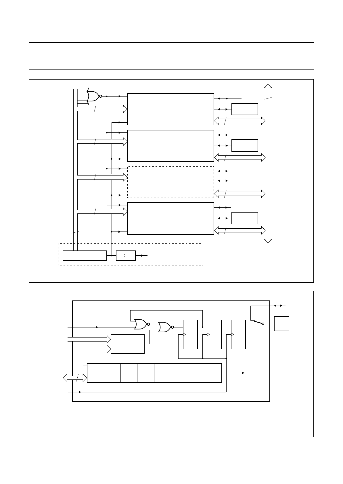
5 BLOCK DIAGRAM
handbook, full pagewidth
V
DD
XTAL1
(IN)
XTAL2
(OUT)
RST
T0
8-BIT
TIMER /
EVENT
COUNTER
80C51
core
excluding
ROM / RAM
CPU
INT0INT1
ROM
(1)
PARALLEL
I / O
PORTS
RAM
256 bytes
8 x 6-BIT PWM
VID1
BF
VID2
DISPLAY
RAM
128 × 10
VCTRL
VID0
VCLK2
OSD BLOCK
14-BIT
PWM
83C145; 83C845
83C055; 87C055
VCLK1
CHARACTER
GENERATOR
60 × 18 × 14
8-bit internal bus
HSYNC
VSYNC
ROM
SOFTWARE
CONTROL
ADC
V
SS
8884
P3 P2 P1
(1) ROM sizes: see Table 1.
8
PWM0 to PWM7
P0
TDAC
3
ADI2 to ADI0
MBE766
Fig.1 Block diagram.
5.1 Part options
Table 1 Differences between the types
TYPES
MEMORY
83C845 83C145 83C055 87C055
ROM 8 kbytes 12 kbytes 16 kbytes −
EPROM (OTP) −−−16 kbytes
1996 Mar 22 4
Page 5

Philips Semiconductors Product specification
Microcontrollers for TV and video (MTV)
6 PINNING INFORMATION
6.1 Pinning
handbook, halfpage
VPP/TDAC/P0.0
handbook, halfpage
PROG/PWM1/P0.1
ASEL/PWM2/P0.2
PWM3/P0.3
PWM4/P0.4
PWM5/P0.5
PWM6/P0.6
PWM7/P0.7
ADI0/P1.0
ADI1/P1.1
ADI2/P1.2
PWM0/P1.3
P2.7
P2.6
P2.5
P2.4
P2.3
P2.2
P2.1
P2.0
V
SS
1
2
3
4
5
6
7
8
9
10
11
12
13
14
15
16
17
18
19
20
83C145
83C845
83C055
87C055
MBE765
42
41
40
39
38
37
36
35
34
33
32
31
30
29
28
27
26
25
24
23
2221
V
DD
P3.7
P3.6
P3.5
P3.4
P3.3/INT0
P3.2/T0
P3.1/INT1
P3.0
RST
XTAL2
XTAL1
BF
VCLK2
VCLK1
VSYNC
HSYNC
VCTRL
VID2
VID1
VID0
83C145; 83C845
83C055; 87C055
Fig.2 Pin configuration (SOT270-1).
1996 Mar 22 5
Page 6

Philips Semiconductors Product specification
Microcontrollers for TV and video (MTV)
83C145; 83C845
83C055; 87C055
6.2 Pin description
Table 2 Pin description SDIP42 (SOT270-1)
SYMBOL PIN DESCRIPTION
Port 0 (notes 1, 2 and 4)
P0.0/TDAC/V
P0.1/PWM1/PROG 2 P0.1: open-drain bidirectional port line;
P0.2/PWM2/ASEL 3 P0.2: open-drain bidirectional port line;
P0.3/PWM3
to
P0.7/PWM7
Port 1 (notes 1, 2 and 5)
P1.0/ADI0
to
P1.2/ADI2
P1.3/PWM0 12 P1.3: open-drain bidirectional port line; PWM0: output for the 6-bit lower-precision
PP
1 P0.0: open-drain bidirectional port line;
TDAC: output for the 14-bit high-precision PWM;
VPP: 12 V programming supply voltage during EPROM programming.
PWM1: output for the 6-bit lower-precision PWM;
PROG: input for EPROM programming pulses.
PWM2: output for the 6-bit lower-precision PWM;
ASEL: input indicating the EPROM address bits that are applied to Port 2.
4to8 P0.3 to P0.7: 5 open-drain bidirectional port lines;
PWM3 to PWM7: 5 outputs for the 6-bit lower-precision PWM.
9to11 P1.0 to P1.2: 3 open-drain bidirectional port lines;
ADI0 to ADI2: inputs for the software analog-to-digital facility.
PWM. PWM0 can be externally pulled up as high as +12 V ±5%
Port 2
P2.7 to P2.0 13 to 20 Port 2: 8-bit open-drain bidirectional port; P2.3 to P2.0 have high current capability
(10 mA at 0.5 V) for driving LEDs. Port 2 pins that have logic 1s written to them float,
and in that state can be used as high-impedance inputs. Any of the Port 2 pins are
driven LOW if the port register bit is written as a logic 0. The state of the pin can
always be read from the port register by the program.
Port 3 (note 1 and 3)
P3.0 34 P3.0: open-drain bidirectional port line.
P3.1/INT1 35 P3.1: open-drain bidirectional port line; INT1: External interrupt 1.
P3.2/T0 36 P3.2: open-drain bidirectional port line; T0: Timer 0 external input.
P3.3/INT0 37 P3.3: open-drain bidirectional port line; INT0: External interrupt 0.
P3.4 to P3.7 38 to 41 P3.4 to P3.7: 4 open-drain bidirectional port lines.
General
V
SS
VID2 to VID0 22 to 24 Digital Video bus: Three totem-pole outputs comprising digital RGB (or other colour
VCTRL 25 Video Control: A totem-pole output indicating whether the OSD facility is currently
21 Ground: 0 V reference.
encoding) from the OSD facility. The polarity of these outputs is controlled by a
programmable register bit (register OSCON; bit Po).
presenting active video on the VID2 to VID0 outputs. Signal is used to control an
external multiplexer (mixer) between normal video and the video derived from VID2 to
VID0. The polarity of this output is controlled by a programmable register bit (register
OSCON; bit Pc).
1996 Mar 22 6
Page 7

Philips Semiconductors Product specification
Microcontrollers for TV and video (MTV)
83C145; 83C845
83C055; 87C055
SYMBOL PIN DESCRIPTION
HSYNC 26 Horizontal Sync: A dedicated input for a TTL-level version of the horizontal sync
pulse. The polarity of this pulse is programmable; its trailing edge is used by the OSD
facility as the reference for horizontal positioning.
VSYNC 27 Vertical Sync: A dedicated input for a TTL-level version of the vertical sync pulse. The
polarity of this pulse is programmable, and either edge can serve as the reference for
vertical timing.
VCLK1 28 VCLK1: Video Clock 1; input for the horizontal timing reference for the OSD facility.
VCLK2 29
BF 30 Background/Foreground: A totem-pole output which, when VCTRL is active,
XTAL1 31 XTAL1: Input to the inverting (oscillator) amplifier and clock generator circuit that
XTAL2 32
RST 33 Reset: If this pin is HIGH for two machine cycles (24 oscillator periods) while the
V
DD
Notes
1. Port 0, Port 1 , and Port 3 pins that have logic 1s written to them float, and in that state can be used as
high-impedance inputs.
2. The state of the pin can always be read from the port register by the program.
3. P3.0, P3.4, and P3.7 can be externally pulled up as high as +12 V ±5%; while P3.5 and P3.6 have 10 mA drive
capability.
4. For each PWM block, a register bit (register PWMn; bit PWnE; n = 0 to 7) controls whether the corresponding pin is
controlled by the block or by Port 0; Port 0 controls the pin immediately after a reset. Regardless of how each pin is
controlled, it can be externally pulled up as high as +12 V ±5%.
5. Any of the Port 1 pins are driven LOW if the corresponding port register bit is written as a logic 0, or for P1.3 only, if
the TDAC module presents a logic 0.
VCLK2: Video Clock 2; output from the on-chip video oscillator. VCLK1 and VCLK2
are intended to be used with an external LC circuit to provide an on-chip oscillator. The
period of the video clock is determined such that the width of a pixel in the OSD is
equal to the inter-line separation of the raster.
indicates whether the current video data represents a Foreground (LOW) or
Background (HIGH) dot in a character. This signal can be used to reduce the intensity
of the background colour and thus emphasize the text.
provides the timing reference for all 83C055 logic other than the OSD facility.
XTAL2: Oscillator output terminal for system clock. XTAL1 and XTAL2 can be used
with a quartz crystal or ceramic resonator to provide an on-chip oscillator. Alternatively,
XTAL1 can be connected to an external clock, and XTAL2 left unconnected.
oscillator is running, the MTV is reset. This pin is also used as a serial input to enter a
test or EPROM programming mode, as on the 87C751.
42 Power supply: for normal and Power-down operation.
1996 Mar 22 7
Page 8

Philips Semiconductors Product specification
Microcontrollers for TV and video (MTV)
7 DESCRIPTION OF STANDARD FUNCTIONS
For a description of the standard functions please refer to
the
“Data Handbook IC20; Section 2: 80C51 Technical
Description”
8 INPUT/OUTPUT (I/O)
The I/O structure of the 83C055 is similar to the standard
I/O structure in the 80C51, except for the points described
in Table 5.
9 DESCRIPTION OF DERIVATIVE FUNCTIONS
9.1 General description
Although the 83C055 is specifically referred to throughout
this data sheet, the information applies to all the devices.
The differences to 80C51 features and the derivative
functions are described in the following Sections and
Chapters.
Figure 1 shows the block diagram of the 83C055.
9.1.1 N
Standard functions to the 80C51 that are not implemented
in the 83C055:
• As Data and Program Memory are not externally
expandable on the 83C055, the ALE, EA, and
PSEN signals are not implemented.
• Idle mode.
• Power-down mode.
.
OT IMPLEMENTED FUNCTIONS
83C145; 83C845
83C055; 87C055
• The IP register is not used, and the IE register (address
A8H) is similar to that on the 80C51;see Table 36.
• The VSYNC input used by the OSD facility can generate
an interrupt. The active polarity of the pulse is
programmable (see Section 13.7); interrupt occurs at
the leading edge of the pulse.
• Since there is no serial port, there are no interrupts nor
control bits relating to this interrupt. The interrupts and
their vector addresses are shown in Table 3.
• External Interrupt 1 is modified so that an interrupt is
generated when the input switches are in either direction
(on the 80C51, there is a programmable choice between
interrupt on a negative edge or a LOW level on INT1).
This facility allows for software pulse-width
measurement handling of a remote control.
Table 3 Program Memory address
EVENT PROGRAM MEMORY ADDRESS
Reset 000H
External INT0 003H
Timer 0 00BH
External INT1 013H
Timer 1 01BH
VSync Start 023H
9.1.3 PCON REGISTER DIFFERENCE
The PCON register format is shown in Table 4. Bits GF1
and GF0 are general purpose flag bits.
9.1.2 I
The interrupt facilities of the 83C055 differ from those of
the 80C51 as follows:
9.1.4 I/O PORTS DIFFERENCES
Table 5 I/O ports differences
Port 0 external memory expansion 8-bit open-drain bidirectional port; and includes:
Port 1 8-bit general purpose quasi-bidirectional 4-bit open-drain port, and includes alternative uses
Port 2 quasi-bidirectional and can be used for external
Port 3 quasi-bidirectional; all eight bits have alternate uses 3 port bits have some of the same alternative uses
1996 Mar 22 8
NTERRUPT FACILITIES DIFFERENCES
I/O STANDARD 80C51 83C055
memory expansion
Table 4 PCON Register format (address 87H)
76543210
−−−−GF1 GF0 −−
alternative use for PWM outputs
for analog inputs and a PWM output
open-drain and general purpose
as on the 80C51 but not necessarily on the same
pins; 5 pins are open-drain and general purpose
Page 9

Philips Semiconductors Product specification
Microcontrollers for TV and video (MTV)
10 6-BIT PWM DACS
Figure 3 shows the 6-bit PWM DAC logic circuit, consisting
of 8 PWMn modules.
The basic MCU clock is divided by 4 to get a waveform that
clocks a 14-bit counter which is common to all the PWMs
(including the 14-bit PWM). This divided clock is hereafter
called the PWM clock.
As illustrated in Fig.3, the lower-precision (6-bit) PWMs
use the least significant part of the 14-bit counter.
Figure 4 shows the circuit diagram of a 6-bit PWM module.
Each PWM module has a Special Function Register
PWMn; n = 0 to 7. The register format is shown in Table 6.
10.1 PWM DAC operation
Value field PVn5 to PVn0 of each PWMn register
(n = 0 to 7) is compared to the 6 LSBs of the common
counter (14-bit counter).
83C145; 83C845
83C055; 87C055
When the value matches, the output flip-flop is cleared, so
that the output pin is driven LOW.
When the value rolls over to zero, the output flip-flop is set,
so that the output pin is released. Thus the output
waveform has a fixed period of 64 PWM clock cycles; its
duty cycle is determined by contents of PWMn.5 to
PWMn.0 (PVn5 to PVn0).
Three of the nine total PWM modules (8 PWMn and the
14-bit PWM DAC) operate as previously described; for
three others, both the rising and falling edges of the output
are delayed by one PWM clock; for the remaining three,
both edges are delayed by two PWM clocks. This feature
reduces the radio-frequency emission that would
otherwise occur when the counter rolled over to zero and
all nine open-drain outputs were released.
10.2 Special Function Register PWMn (n = 0 to 7)
Table 6 Special Function Register PWMn (n = 0 to 7; addresses D4H to DFH)
7 6 5 4 3 2 1 0
PWnE − PVn5 PVn4 PVn3 PVn2 PVn1 PVn0
Table 7 Description of PWMn bits
BIT SYMBOL DESCRIPTION
7 PWnE PWM module enable bit. If for a particular PWM block (n) the bit:
PWnE = 1, then the block is active and controls its assigned port pin.
PWnE = 0, the corresponding port pin is controlled by the port.
6 − Reserved.
5 to 0 PVn5 to PVn0 Value field for PWMn register.
1996 Mar 22 9
Page 10
Philips Semiconductors Product specification
Microcontrollers for TV and video (MTV)
handbook, full pagewidth
ZERO
6
1st PWM MODULE (n = 0)
6
2nd PWM MODULE (n = 1)
6
3rd to 7th PWM MODULE (n = 2 to 6)
6
8th PWM MODULE (n = 7)
6
8
8
8
8
83C145; 83C845
83C055; 87C055
P1.3
PWM0/P1.3
P0.1
PWM1/P0.1
P0.2 to P0.6
PWM2/P0.2
to
PWM6/P0.6
P0.7
PWM7/P0.7
8
LS 6-bits PWM clock
14-BIT COUNTER
handbook, full pagewidth
(1) This flip-flop occurs in 5 of the 8 PWMn modules.
(2) This flip-flop occurs in 3 of the 8 PWMn modules.
PWM module (n)
ZERO
LS 6-bits
6-bits (PVn0 to PVn5)
8
PVn0 PVn1 PVn2 PVn3 PVn4 PVn5 PWnE
internal bus
PWM clock
4
6-bit
COMPARATOR
f
xtal
14-BIT PWM
DAC BLOCK
Fig.3 6-bit PWM DAC logic circuit.
MBE771 - 1
(1) (2)
internal bus
I/O port
MBE770
PWMn
I/O pin
Fig.4 A 6-bit PWM module.
1996 Mar 22 10
Page 11

Philips Semiconductors Product specification
Microcontrollers for TV and video (MTV)
11 14-BIT PWM DAC (TDAC)
11.1 14-bit counter
The 14-bit counter was already mentioned in Section 10.
The nature of the counter is such that it can achieve a
stable output value through its MSB, and the value can
propagate through logic like that shown in Fig.5. The logic
output can be stable within:
• one period of the PWM clock (e.g. 250 ns) if
edge-triggered logic is used to capture the logic output,
or
• one phase of the PWM clock (e.g. 125 ns) if a phase of
the PWM clock is used to capture the logic output.
The 14-bit (TDAC) counter is a ripple counter (cost and
die-size reasons).
The 14-bit PWM DAC is controlled by two special function
registers TDACL and TDACH.
11.2 14-bit DAC operation
When software wishes to change the 14-bit value
(TD0 to TD13), it should first write to TDACL and then
write to TDACH. Alternatively, if the required precision of
the duty cycle is satisfied by 6 bits or less, software can
simply write to TDACH (TD8 to TD13).
11.2.1 L
Figure 5 shows that this block includes an ‘extra’ 14-bit
latch between TDACL - TDACH and the comparator and
other logic. The programmed value is clocked into the
operative latch when the 7 low-order bits of the counter roll
over to zero, provided that the software is not in the midst
of loading a new 14-bit value, i.e. it is not between writing
TDACL and writing TDACH.
In a similar fashion to the lower-precision PWMs, this
facility has an output flip-flop that is set when the lower
7 bits of the counter overflow/wrap. The more significant
7 bits of the operative latch’s programmed value are
compared for equality against the less significant 7 bits of
the counter, and the output FF is cleared when they match.
Thus this output has a fixed period of 128 PWM clock
cycles, and the duty cycle is determined by the
programmed value.
OW PRECISION OPERATION
83C145; 83C845
83C055; 87C055
11.2.2 H
For the higher-precision aspect of this feature, the 7 MSBs
of the counter are used in a logic block with the 7 LSBs of
the programmed value.
The 7th LSB (binary value 64) of the programmed value is
ANDed with the 7th MSB (128) of the counter, the 6th LSB
of the value is ANDed with the counter’s 6th and 7th MSBs
being 10, and so on through the LSB of the programmed
value being ANDed with the counter’s 7 MSBs being
100000. Then these 7 ANDed terms are ORed. If the
result is true (logic 1) at the time the 7 LSBs of the counter
match the MSBs of the programmed value, the output is
forced high for 1 (additional) PWM clock cycle.
The result is that, if the value-64 bit of the 14-bit value is
programmed to a logic 1, every other cycle of 128 PWM
counter clocks has its duty cycle stretched by one counter
clock; if the value-32 bit is programmed to logic 1, every
th
cycle is stretched, and so on through, if the value-1 bit
4
is programmed to logic 1, one cycle out of each 128 is
stretched.
11.2.3 14Assuming the external integrator can handle all this, the
net effect is a PWM DAC that has the period of a 7-bit
design (which makes the integrator easier and more
feasible to design) with the accuracy of a 14-bit one.
An obvious prerequisite for such precision is that the load
on the voltage must be very light, like a single op-amp or
comparator.
11.2.3.1 Note
The TDAC feature differs from the corresponding features
of predecessor parts in several ways:
1. The 14-bit value is functionally composed of major and
2. The 14-bit value is programmed as a contiguous
3. As discussed for the 6-bit DACs, both of the preceding
IGH PRECISION OPERATION
BIT DAC OUTPUT
minor portions of 7 bits each.
multi-register value that can be manipulated
straight-forwardly via arithmetic instructions.
parts had a feature whereby the PWM output could be
inverted, redundantly with complementing the 14-bit
value. This feature has been eliminated.
1996 Mar 22 11
Page 12

Philips Semiconductors Product specification
Microcontrollers for TV and video (MTV)
83C145; 83C845
83C055; 87C055
11.3 Special Function Register TDACL
Table 8 Special Function Register TDACL format (address D2H)
76543210
TD7 TD0 TD1 TD2 TD3 TD4 TD5 TD6
Table 9 Description of TDACL bits
BIT SYMBOL DESCRIPTION
7 to 0 TD7, TD0 to TD6 8 LSBs of the 14-bit value.
11.4 Special Function Register TDACH
Table 10 Special Function Register TDACH format (address D3H)
76543210
TDE − TD13 TD12 TD11 TD10 TD9 TD8
Table 11 Description of TDACH bits
BIT SYMBOL DESCRIPTION
7 TDE Enable bit.
6 − Reserved.
5 to 0 TD13to TD8 6 MSBs of the 14-bit value.
1996 Mar 22 12
Page 13

Philips Semiconductors Product specification
Microcontrollers for TV and video (MTV)
handbook, full pagewidth
77
TDACH
8
7 MSB
7-BIT COMPARATOR
7
7
14-BIT LATCH
TDACL
7 LSB
8
88
7
83C145; 83C845
83C055; 87C055
INTERNAL BUS
7 LSB
7
14-BIT COUNTER
7
7 MSB
PWM clock
TDACH.7
TDAC/
P0.0
P0.0
4
f
xtal
MBE774
Fig.5 14-bit PWM logic circuit.
1996 Mar 22 13
Page 14

Philips Semiconductors Product specification
Microcontrollers for TV and video (MTV)
83C145; 83C845
83C055; 87C055
12 SOFTWARE ANALOG-TO-DIGITAL FACILITY
Figure 6 shows the software analog-to-digital facility block diagram. The block includes Special Function Register SAD.
12.1 Special Function Register SAD
Table 12 Special Function Register SAD format (address D8H)
76543210
VHi CH1 CH0 St SAD3 SAD2 SAD1 SAD0
Table 13 Description of SAD bits
BIT SYMBOL DESCRIPTION
7 VHi The comparator output bit; bit addressable.
6 CH1 The channel field controls which pin, if any, is connected to this facility; see Table 14.
5 CH0
4 St The St bit should be written as a logic 1 in order to initiate a voltage comparison.
3 to 0 SAD3 to SAD0 4 LSBs of the SAD register.
12.2 Software ADC operation
Port pins P1.0/ADI0 to P1.2/ADI2 can be alternately
selected as inputs of a linear voltage comparator. The
other input of the comparator is connected to a 4-bit DAC.
This DAC is controlled by bits SAD3 to SAD0 and
produces a reference voltage:
nominally 0.15625 to 4.84375 V in increments of
0.3125 V.
The output of the comparator (HIGH or LOW) can be read
by the program as the MSB of the SAD register i.e. bit VHi.
After writing St = 1, the program should include intervening
instructions totalling at least 6 machine cycles (72 clock
periods or 6 µs at 12 MHz), before the instruction that
accesses and tests VHi.
Table 14 Pin selection: P1.n/ADIn
CH1 CH0 P1.n/ADIn
0 0 none
0 1 P1.0/ADI0
1 0 P1.1/ADI1
1 1 P1.2/ADI2
Note
1. Port 1 has open-drain drivers which will not materially
affect an analog voltage as long as any and all pins
used for software analog-to-digital measurement have
corresponding logic 1s in the port register; n = 0, 1, 2.
(1)
1996 Mar 22 14
Page 15

Philips Semiconductors Product specification
Microcontrollers for TV and video (MTV)
internal bus
I/O PORT
I/O PORT
I/O PORT
ANALOG
MUX
SAD.6:5 SAD.3:0
handbook, full pagewidth
P1.0/ADI0
P1.1/ADI1
P1.2/ADI2
4-BIT
DAC
VOLTAGE
COMPARATOR
83C145; 83C845
83C055; 87C055
MBE772
Fig.6 Software analog-to-digital facility.
1996 Mar 22 15
Page 16

Philips Semiconductors Product specification
Microcontrollers for TV and video (MTV)
13 ON SCREEN DISPLAY (OSD)
Figure 7 shows the OSD block diagram. It shows the CPU
writing into the 128 × 10 display RAM, which is dual-ported
to allow the CPU to write into it at any time, including when
it is being read out by the OSD logic. The 10-bit wide data
coming out of the display RAM is used to access the
appropriate character in the Character Generator memory
(6-bits) and to specify character and display control
functions (4-bits).
Timing for the OSD is controlled by the HSYNC, VSYNC,
and dot clock input VCLK1.
13.1 OSD features
The 83C055 features an advanced OSD function with
some unique features as described in Sections 13.1.1 to
13.1.10.
13.1.1 U
The OSD does not restrict the user to a fixed number of
lines with a fixed number of characters per line:
• Using a fixed number of lines restricts the generation of
displays that can be differentiated from others that use
the same chip and places limits on screen content.
• Using a fixed number of characters per line wastes
display RAM if a line has less than the full number of
displayable characters (it has to be padded with
non-visible characters).
SER-DEFINABLE DISPLAY FORMAT
83C145; 83C845
83C055; 87C055
13.1.3 D
The OSD has a true display RAM instead of a character
line buffer. This display RAM is dual-ported to allow
updating the display RAM at any time instead of having to
wait for a vertical retrace.
Vertical Sync (VSYNC) interrupts are supported if
flicker-free updates are required.
13.1.4 P
• Normal characters are displayed as 18 × 14 bit maps.
• In an interlaced display:
– 2 fields are displayed so that one actually sees a
– The part has a double height and width mode which
• For use in non-interlaced systems, the part has a double
height mode so that the displayed characters have the
same pixel size (36 × 14) as on an interlaced display.
13.1.5 C
When characters are displayed overlaid on a background
of base video, a black border around the characters makes
them highly legible. This feature is called shadowing. The
83C055 has 8 shadowing modes to allow the user to select
various partial shadow modes as well as full surround
shadow; see Fig.8 and Table 28.
UAL-PORTED DISPLAY RAM
ROGRAMMABLE CHARACTER SIZE
36 × 14 pixel size character.
displays 36 × 28 pixel size bit maps per field.
HARACTER SHADOWING
The OSD on the 83C055 defines a control character:
• New Line, that has the same function as a Carriage
Return and Line Feed.
When the OSD circuitry fetches this character from display
RAM it stops displaying further characters, waits for the
next horizontal scan line, and starts displaying the next
character in display RAM after the New Line character was
received.
The number of lines is thus up to the user, within the limits
of the display and memory, as are the number of
characters per line. This allows far better control of the
appearance of the OSD.
13.1.2 C
OLOURS SELECTABLE BY CHARACTER
Characters can be displayed on a background of the base
video or a programmable background colour.
The background colour is selectable by word and the
choice of background (base video/user programmed
colour) by character.
1996 Mar 22 16
13.1.6 P
ROGRAMMABLE POLARITIES
Inputs to and outputs from the OSD can be programmed
to be recognized as active LOW or HIGH. In conjunction
with the 12 V outputs, this allows direct interfacing to most
video signal processing circuits.
13.1.7 C
HARACTER GENERATOR MEMORY IN EPROM
On the 87C055, the Character Generator memory is in
EPROM. This feature allows quick and inexpensive font
development and refinement against the alternative of
creating a masked ROM version to see how the final fonts
will appear.
13.1.8 HSYNC
LOCKED DOT CLOCK OSCILLATOR
The 83C055 is designed to use an LC oscillator circuit that
is started at the trailing edge of HSYNC and stopped at its
leading edge. In practice, this gives a highly consistent
delay from HSYNC to oscillator start and is stable from
scan line to scan line so that no left margin effects are
seen.
Page 17

Philips Semiconductors Product specification
Microcontrollers for TV and video (MTV)
13.1.9 SHORT ROWS
This mode only displays 4 horizontal lines and is used for
generating underlines.
13.1.10 PROGRAMMABLE HORIZONTAL AND VERTICAL
POSITIONS
Bit pairs HS4 to HS0 and VS2 to VS0 in register OSORG
(Table 30) define the starting point of the display.
13.2 General description of the OSD module
This block is the largest of the additions that are specific to
this product. Its basic function is to superimpose text on
the television video image, to indicate various parameters
and settings of the receiver or tuner. External circuitry
handles the mixing (multiplexing) of the text and the TV
video. The OSD block has 4 input pins:
• Two for a video clock: VCLK1 and VCLK2
• Horizontal sync signal: HSYNC
• Vertical sync signal: VSYNC.
The block has 4 outputs:
• 3 colour video signals
• a control signal.
Since this block is the major feature of the part, its main
inputs and outputs are dedicated pins, without alternate
port bits. The OSD of the 83C055 differs from that in
preceding devices in one major way:
• It does not fix the number and size of displayed rows of
text.
Several predecessor parts allowed two displayed rows of
16 characters each. The 83C055 simply has 128 locations
of Display RAM, each of which can contain:
• a displayed character, or
• a New Line character that indicates the end of a row.
A variant of the New Line character is used to indicate
the end of displayed data.
A number of changes in the OSD architecture have
reduced the number of other Special Function Registers
involved in the feature, below the number needed with
predecessor devices:
1. The elimination of certain options such as 4, 6, or
8 × character sizes and alternate use of two of the
video outputs.
2. The moving of certain other options from central
registers to Display RAM, such as foreground colour
codes (Fcolor) and background (B) selection.
83C145; 83C845
83C055; 87C055
Figure 7 shows the 3 major elements of the OSD facility:
• OSD logic
• Display RAM
• Character Generator ROM.
13.3 OSD logic
For a standard NTSC TV signal with an HSYNC frequency
of 15.750 kHz and a VSYNC frequency of nominally
60 Hz, there are roughly 50 µs of active horizontal scan
line available.
A typical pixel clock frequency is 8 MHz, and therefore
roughly 400 pixels of resolution can be obtained. At
14 dots per character, this means 28 character per
horizontal scan line. If the 12 dot per character display
mode is used, that means 33 character per horizontal scan
line. Allowing for edge effects, 26 characters (14 across) or
31 characters (12 across) can be displayed.
Note that VGA rates and higher can be used. The
minimum character dot size will be a function of the VGA
frequency used. For a 640 × 480 display, running at
33 kHz, the equivalent 83C055 pixel resolution is about
160 across (because of the 8 MHz clock and allowing for
overscan). This means that status and diagnostic
information can be displayed on video monitors.
13.3.1
The video clock pins (VCLK1 and VCLK2) are used to
connect a LC circuit to an on-chip video oscillator that is
independent of the normal MCU clock.
The L and C values are chosen so that a video pulse, of a
duration equal to the VCLK period, will produce a
more-or-less square dot on the screen, that is, a dot having
a width approximately equal to the vertical distance
between consecutive scan lines.
The video oscillator is stopped (with VCLK2 = LOW) while:
• HSYNC (Horizontal Sync) is maintained, and
• is released to operate at the trailing edge of HSYNC.
This technique helps provide uniform horizontal
positioning of characters/dots from one scan line to the
next.
ON-CHIP VIDEO OSCILLATOR
1996 Mar 22 17
Page 18

Philips Semiconductors Product specification
Microcontrollers for TV and video (MTV)
13.4 Character Generator ROM
Character Generator ROM. Containing 60 displayable bit
maps, i.e. 64 minus 4, comprising:
• One for each of new line: New Line, and
• Three space characters:
– Space
– BSpace
– SplitBSpace.
Each bit map includes 18 scan lines by 14 dots.
The Character Generator ROM is maskable or
programmable along with the Program ROM to allow for
various character sets and languages.
book, full pagewidth
HSYNC
OSD LOGIC
VSYNC
83C145; 83C845
83C055; 87C055
13.5 Display RAM organization
Each Display RAM location includes:
• 6 data bits, and
• 4 attribute bits.
The 6 data bits from Display RAM, along with a
line-within-row count, act as addresses into the Character
Generator ROM. Except in special test modes that are
beyond the scope of this data sheet, Display RAM cannot
be read by the MCU program.
VCLK2
VCLK1
internal
bus
7
7
OSD RAM
128 × 10
6
CHARACTER
GENERATOR
ADDRESS LOGIC
4
6
ATTRIBUTE
CONTROL
CHARACTER
GENERATOR
60 × 18 × 14
Fig.7 OSD block diagram.
RGB
DIGITAL
VIDEO OUT
MBG323
VCTRL
VID2
VID1
VID0
1996 Mar 22 18
Page 19

Philips Semiconductors Product specification
Microcontrollers for TV and video (MTV)
83C145; 83C845
83C055; 87C055
13.6 OSD Special Function Registers
The programming interface to Display RAM is provided by
three Special Function Registers as shown in Tables 15,
17 and 20.
Writing OSAT simply latches the attribute bits into a
register, while writing OSDT causes the data bus
information, plus the contents of the OSAT register, to be
written into display RAM.
Thus, for a given Display RAM location, OSAT should be
written before OSDT. If successive characters are to be
written into Display RAM with the same attributes, OSAT
13.6.1 S
Table 15 Special Function Register OSAD (On Screen ADdress; address 9AH)
PECIAL FUNCTION REGISTER OSAD
76543210
−OSAD6 OSAD5 OSAD4 OSAD3 OSAD2 OSAD1 OSAD0
need not be rewritten for each character, only prior to
writing OSDT for the first character with those particular
attributes.
The OSAT attribute bits associated with the BSpace,
SplitBSpace and New Line characters (see Table 19) are
interpreted differently from those that accompany other
data characters. With BSpace and SplitBSpace, B is
interpreted as described above, but the 3 colour bits
specify the background colour (Bcolor) for subsequent
characters. For BSpace, a change in B and Bcolor
becomes effective at the left edge of the character’s bit
map.
Table 16 Description of OSAD bits
BIT SYMBOL DESCRIPTION
7 − Reserved.
6 to 0 OSAD6 to OSAD0 These 7-bits hold the Display RAM address into which data will be
loaded. OSAD is automatically incremented by one each time OSDT and
Display RAM are written to.
13.6.2 S
Writing OSDT causes the data bus information, plus the contents of the OSAT register, to be written into display RAM.
Table 17 Special Function Register OSDT (On Screen DaTa; address 99H)
Table 18 Description of OSDT bits
PECIAL FUNCTION REGISTER OSDT
76543210
−−OSDT5 OSDT4 OSDT3 OSDT2 OSDT1 OSDT0
BIT SYMBOL DESCRIPTION
7to6 − Reserved.
5 to 0 OSDT5 to OSDT0 Character data; see Table 19. In reality, there is a potential conflict
between the timing of a write to OSDT and an access to display RAM by
the OSD logic for data display. This is resolved by the use of a true
dual-ported RAM for display memory.
1996 Mar 22 19
Page 20

Philips Semiconductors Product specification
Microcontrollers for TV and video (MTV)
83C145; 83C845
83C055; 87C055
Table 19 Special characters related to OSDT register
SPECIAL CHARACTER OSDT5 OSDT4 OSDT3 OSDT2 OSDT1 OSDT0
New Line 1 1 1 1 0 1
Space (normal) 1 1 1 1 0 0
BSpace 1 1 1 1 1 0
SplitBspace 1 1 1 1 1 1
13.6.3 S
Table 20 Special Function Register OSAT ( OnScreen ATtributes; address 98H)
New Line −−−E−SR D Sh
BSpace −−−B−BC2 BC1 BC0
SplitBSpace −−−B−BC2 BC1 BC0
Any other character −−−B−FC2 FC1 FC0
Table 21 Description of OSAT bits
PECIAL FUNCTION REGISTER OSAT
WITH OSDT = 76543210
BIT SYMBOL DESCRIPTION
7 to 5, 3 − Reserved.
With OSDT = New Line; note 1
4 E End; If the E bit is 1, no further rows are displayed on the screen.
2 SR Short row; If E = 0 and SR = 1, the next row is a ‘short row’, i.e. it is only 4 or 8 scan lines high
rather than 18 or 36. Short rows can be used for underlined text.
1 D Double height; If E = 0 and D = 1, all of the characters in the following row are displayed with
‘double height and width’.
0 Sh Shadowing; If E = 0 and Sh = 1, all of the characters in the following row are displayed with
‘shadowing’; see Section 13.8.
With OSDT = BSpace or SplitBspace; note 2
4 B Background; B indicates whether ‘background pixels’ should show the current background
colour (B = 1), or television video (B = 0).
2 to 0 BC2 to BC0 Bcolor: Background colour (notes 3 and 4; see Table 22).
With OSDT = Any other character
4 B Background; B indicates whether ‘background pixels’ should show the current background
colour (B = 1), or television video (B = 0).
2 to 0 FC2 to FC0 Fcolor: Foreground colour. Fcolor indicates the colour of ‘foreground pixels’ in the ROM bit
map for this character (see Table 22).
1996 Mar 22 20
Page 21

Philips Semiconductors Product specification
Microcontrollers for TV and video (MTV)
83C145; 83C845
83C055; 87C055
Notes to the description of OSAT bits
1. The latches in which the E,SR, D, and Sh bits are captured are cleared to zero at the start of each vertical scan. This
means that if the first text line on the screen is a short row, or if it contains either double size or shadowing, the text
must be preceded by a New Line character. Like all such characters, this initial New Line advances the vertical
screen position; the VStart value (see register OSORG; Section 13.9) should take this fact into account.
2. For SplitBSpace, a change in B and Bcolor occurs halfway through the character horizontally.
3. The normal Space character has no effect on the Bcolor value.
4. The Bcolor value is not cleared between vertical scans, so that if a single background colour is all that is needed in
an application, it can be set via a single BSpace character during program initialization, and never changed
thereafter. In order for such a BSpace to actually affect the 83C055 internal Bcolor register the Mode field of the
OSMOD register must be set to ‘01B’ (or higher) so that the OSD hardware is operating (see register OSMOD;
Section 13.8).
Table 22 OSD outputs related to character bit map value, Fcolor, Bcolor and B bits
CHARACTER BIT MAP VALUE
VID2 VID1 VID0 VCTRL
logic 1 FC2 FC1 FC0 driven active
logic 0 BC2 BC1 BC0 B
OSD OUTPUTS (notes 1 and 2)
Notes
1. Bcolor (BC2,BC1,BC0) values ‘000’ and ‘111’ minimize the occurrence of transient states among the VID2 to VID0
outputs.
2. The background colour defined by the most recently encountered BSpace or SplitBSpace character is maintained
on the VID2 to VID0 pins except at the following times:
a) During the active time of HSYNC.
b) During the active time of VSYNC.
c) During those pixels of an active character that correspond to a logic 1 in the character’s bit map.
d) During a ‘shadow’ bit.
1996 Mar 22 21
Page 22

Philips Semiconductors Product specification
Microcontrollers for TV and video (MTV)
83C145; 83C845
83C055; 87C055
13.7 OSD Control Register OSCON
Table 23 OSD Control Register OSCON (address C0H)
76543210
IV Pv Lv Ph Pc Po DH BFe
Table 24 Description of OSCON bits (see note 1)
BIT SYMBOL DESCRIPTION
7 IV Interrupt flag for the OSD feature. Bit IV is set by the leading edge of the VSYNC pulse,
and is cleared by the hardware when the VSYNC interrupt routine is vectored to. It can
also be set or cleared by software writing a logic 1 or logic 0 to this bit.
6 Pv Pv defines the active VSYNC input polarity. If Pv = 0, then VSYNC input is active HIGH;
if Pv = 1, then VSYNC input is active LOW.
One effect of bit Pv is that the VID2 to VID0 and VCTRL outputs are blocked (held at
black/inactive) during the active time of VSYNC. The IV bit is set on the leading edge of
the VSYNC pulse; thus Pv controls whether the OSD interrupt occurs in response to a
HIGH-to-LOW or LOW-to-HIGH transition on VSYNC.
5 Lv Lv defines the active edge of VSYNC. The active edge (leading or trailing) of VSYNC
(as defined by Pv), clears the state counter which determines the vertical start of on
screen data. Time reference for the video field is the leading edge of VSYNC, if Lv = 0,
or the trailing edge of VSYNC, if Lv = 1.
4 Ph Ph defines the active HSYNC input polarity. If Ph = 0, then HSYNC input is active HIGH;
if Ph = 1, then HSYNC input is active LOW.
3 Pc Pc defines the active VCTRL output polarity; VCTRL output active means: show the
colour on VID2 to VID0. If Pc = 0, then VCTRL output is active HIGH; If Pc = 1, then
VCTRL output is active LOW.
2 Po Po defines the VID2 to VID0 outputs polarity; bit is needed only because the Shadowing
feature needs to generate black pixels without reference to a register value. Internally,
the 3-bit code ‘000B’ always designates black.
If Po = 0, a logic 0 internal to the 83C055 corresponds to a LOW on one of the
VID2 to VID0 pins.
If Po = 1, a logic 1 internal to the 83C055 corresponds to a LOW on one of the
VID2 to VID0 pins.
1 DH If DH = 1, character sizes are doubled vertically but not horizontally. This feature allows
the 83C055 to be used in ‘improved definition’ systems that are not interlaced.
The vertical doubling imposed by DH does not affect the VStart logic as described in
Table 30; it operates in HSync units regardless of DH or D.
0 BFe Background/Foreground enable; output BF. If BFe = 1, then the BF output tracks
whether each bit in displayed characters is a Foreground bit (LOW), or a Background bit
(HIGH). If BFe = 0, then the BF pin remains HIGH.
Note
1. It is theoretically possible that a VSYNC interrupt could be missed, or an extra one generated, if OSCON is read,
then modified internally (e.g. in ACC), and the result written back to OSCON. However, none of the other bits in
OSCON are reasonable candidates for dynamic change. Special provisions are included in the 83C055 logic so that
IV will not be changed by a single ‘read-modify-write’ instruction such as SETB or CLR, unless the instruction
specifically changes IV.
1996 Mar 22 22
Page 23

Philips Semiconductors Product specification
Microcontrollers for TV and video (MTV)
83C145; 83C845
83C055; 87C055
13.8 OSD Control Register OSMOD
Under some conditions writing to OSMOD while the display is active can cause a temporary flicker during that display
field. This can be avoided by only writing to OSMOD during the vertical sync interval.
Table 25 OSD Control Register OSMOD (address C1H)
76543210
Wc − Mode1 Mode0 − SHM2 SHM1 SHM0
Table 26 Description of OSMOD bits (see note )
BIT SYMBOL DESCRIPTION
7 Wc If Wc = 1, then each displayed character is horizontally terminated after
12 bits have been output, as opposed to after 14 bits if Wc = 0. This
allows text to be ‘packed’ more tightly so that more characters can be
displayed per line. In effect, the 2 bits out of the display ROM, which
would otherwise be the rightmost 2 of the 14, are ignored when Wc is 1.
Clearly, if this feature is to be used, it must be accounted for in the design
of the bit maps in the display ROM.
6 − Reserved.
5 Mode1 Display mode select bits; see Table 27.
4 Mode0
3 − Reserved.
2 to 0 SHM2 to SHM0 Shadowing mode (ShMode); determines how characters are shadowed
in rows for which the row attribute Sh = 1 (register OSAT; see Table 21);
for the shadowing modes see Fig.8 and Table 28.
Table 27 Selection of Display Modes
Mode1 Mode0 DISPLAY MODE
0 0 Mode 0 The OSD feature is disabled. VCLK oscillator is disabled, VID2 to VID0 are set to black, and
VCTRL is held inactive.This is the mode to which the 83C055 OSD logic is reset; note 1.
0 1 Mode 1 The VCLK oscillator is enabled and the OSD logic operates normally internally, but
VID2 to VID0 are set to black and VCTRL is held inactive; note 2.
1 0 Mode 2 Normal OSD operation. Active characters can be shown against TV video (for characters
with B = 0) or (for characters with B = 1) against a background of the colour defined as an
attribute of BSpace and SplitBSpace characters.
1 1 Mode 3 Characters can be displayed but all of the receiver’s normal video is inhibited by holding
VCTRL asserted throughout the active portion of each scan line; see note 3.
Notes
1. A direct transition from this mode to ‘active display’ (Mode1, Mode0 = 1X) would result in undefined operation and
visual effects for the duration of the current video field (until the next VSYNC).
2. The OSD feature can be toggled between this state and ‘active display’ as desired to achieve real-time special effects
such as ‘vertical wiping’.
3. Since VID2 to VID0 are driven with the current background colour during this time, except during the foreground
portion of displayed characters, this produces text against a solid background. This mode is useful for extensive
displays that require user concentration.
1996 Mar 22 23
Page 24

Philips Semiconductors Product specification
Microcontrollers for TV and video (MTV)
83C145; 83C845
83C055; 87C055
Table 28 Shadowing modes determined by bits SHM2 to SHM0 (register OSMOD) and Sh (register OSAT)
SHM2 SHM1 SHM0 Sh SHADOWING MODE
0 0 0 1 South-west
0 0 1 1 West
0 1 0 1 North-west
0 1 1 1 North
1 0 0 1 North-east
1 0 1 1 East
1 1 0 1 South-east
1 1 1 1 Full surround
X X X 0 No Shadowing
Note
1. The mode names are based on the position of an apparent light source, ranging from the lower left (South-west)
clockwise to the lower right (South-east); see Fig.8.
13.9 OSD Control Register OSORG
(1)
Table 29 OSD Control Register OSORG (address C2H)
76543210
HS4 HS3 HS2 HS1 HS0 VS2 VS1 VS0
Table 30 Description of OSORG bits (note 1)
BIT SYMBOL DESCRIPTION
7 to 3 HS4 to HS0 HStart field; defines the horizontal start position of all the on-screen character rows, as
approximately a multiple of 4 VCLK clock cycles. Active display begins after the trailing
edge of HSYNC at the position:
HP 4 HStart()× 1+[]VCLK clock cycle× one single-sized character width()+=
Where (HStart) is the decimal value of bits (HS4 to HS0); note 2.
2 to 0 VS2 to VS0 VStart field; defines the vertical start position of the first on-screen character row, as
approximately a multiple of 4 HSYNC pulses. Active display begins after the field’s time
reference point (a range of 3 to 31)at the position:
VP 4 VStart()× 1–[]HSYNC pulses×=
Where (VStart) is the decimal value of bits (VS2 to VS0); note 3.
Notes
1. Neither the Hstart nor Vstart parameter is affected by the D line attribute that is used to display double-sized
characters.
2. Counting variations in Wc, there may be 17 to 143 VCLK clock cycles from the end of HSYNC to the start of the first
character of each row.
3. Subsequent character rows occur directly below the first, such that the last scan line of one row is directly followed
by the first scan line of the next row. Successive New Line characters (with or without the Short Row designation)
can be used to vertically separate text rows on the screen.
1996 Mar 22 24
Page 25

Philips Semiconductors Product specification
Microcontrollers for TV and video (MTV)
handbook, full pagewidth
83C145; 83C845
83C055; 87C055
foreground
colour pixel
black pixel
background
colour pixel
apparent light
source
ShMode = 100ShMode = 011ShMode = 010
ShMode = (SHM2, SHM1, SHM0)
ShMode = 101No ShadowingShMode = 001
ShMode = 110ShMode = 111ShMode = 000
Fig.8 Effect of shadowing on the letter ‘E’.
MBE773
1996 Mar 22 25
Page 26

Philips Semiconductors Product specification
Microcontrollers for TV and video (MTV)
83C145; 83C845
83C055; 87C055
14 PROGRAMMING CONSIDERATIONS
14.1 EPROM Characteristics
The 87C055 is programmed by using a modified Quick-Pulse Programming algorithm similar to that used for devices
such as the 87C751. It differs from these devices in that a serial data stream is used to place the 87C055 in the
programming mode.
Figure 9 shows a block diagram of the programming configuration for the 87C055.
Table 31 Pin usage for Programming
PIN USAGE
XTAL1 Oscillator input and receives the master system clock. This clock should be between
1.2 and 6 MHz.
RESET Used to accept the serial data stream that places the 87C055 into various programming modes.
This pattern consists of a 10-bit code with the LSB sent first. Each bit is synchronized to the
clock input, XTAL1.
Port 0
/TDAC/P0.0 Used as the programming voltage supply input (VPP signal).
V
PP
PROG/PWM1/P0.1 Used as the program PROG signal. This pin is used for the 25 programming pulses.
Port 2
P2.7 to P2.0 Address input for the byte to be programmed and accepts both the high- and low-order
components of the 11-bit address; note 1.
Port 3
P3.7 to P3.0 Used as a bidirectional data bus during programming and verify operations. During programming
mode, it accepts the byte to be programmed. During verify mode, it provides the contents of the
EPROM location specified by the address which has been supplied to Port 2.
Note
1. Multiplexing of these address components is performed using the ASEL input:
a) ASEL input is driven HIGH and then drive Port 2 with the high-order bits of the address. ASEL should remain
HIGH for at least 13 clock cycles.
b) ASEL may then be driven LOW which latches the high-order bits of the address internally. The high-order address
should remain on Port 2 for at least 2 clock cycles after ASEL is driven LOW.
c) Port 2 may then be driven with the low byte of the address. The low-order address will be internally stable 13 clock
cycles later. The address will remain stable provided that the low byte placed on Port 2 is held stable and ASEL
is kept LOW.
d) ASEL needs to be pulsed HIGH only to change the high byte of the address.
1996 Mar 22 26
Page 27

Philips Semiconductors Product specification
Microcontrollers for TV and video (MTV)
14.2 Programming operation
Figures 10 and 11 show the timing diagrams for the
Program/Verify cycle. Programming operation:
1. RST should initially be held HIGH for at least
2 machine cycles. P0.1 (PROG) and P0.0 (VPP) will be
at VOH as a result of the RST operation. At this point,
these pins function as normal quasi-bidirectional I/O
ports and the programming equipment may pull these
lines LOW. However, prior to sending the 10-bit code
on the RST pin, the programming equipment should
drive these pins HIGH (V
2. The RST pin may now be used as the serial data input
for the data stream which places the 87C055 in the
Programming Mode. Data bits are sampled during the
clock HIGH time and thus should only change during
the time that the clock is LOW. Following transmission
of the last data bit, the RST pin should be held LOW.
3. Next the address information for the location to be
programmed is placed on Port 2 and ASEL is used to
perform the address multiplexing, as previously
described (see Table 31; note 1).
a) At this time, Port 1 functions as an output.
b) A high voltage VPP level is then applied to the V
input (P0.0). This sets Port 1 as an input port.
c) The data to be programmed into the EPROM array
is then placed on Port 3. This is followed by a
series of programming pulses applied to the PROG
pin (P0.1). These pulses are created by driving
P0.1 LOW and then HIGH. This pulse is repeated
until a total of 25 programming pulses have
occurred. At the conclusion of the last pulse, the
PROG signal should remain HIGH.
4. The VPP signal may now be driven to the VOH level,
placing the 87C055 in the Verify Mode; Port 3 is now
used as an output port. After four machine cycles
(48 clock periods), the contents of the addressed
location in the EPROM array will appear on Port 3.
5. The next programming cycle may now be initiated by:
a) Placing the address information at the inputs of the
multiplexed buffers.
b) Driving the VPP pin to the VPP voltage level.
c) Providing the byte to be programmed to Port 3 and
issuing the 26 programming pulses on the PROG
pin.
d) Bringing VPP back down to the VOH level and
verifying the byte (see Table 33).
).
IH
PP
83C145; 83C845
83C055; 87C055
14.3 Erasure Characteristics
Erasure of the EPROM begins to occur when the chip is
exposed to light with wavelengths shorter than
approximately 4000 Angstroms. Since sunlight and
fluorescent lighting have wavelengths in this range,
exposure to these light sources over an extended time
(about 1 week in sunlight, or 3 years in room level
fluorescent lighting) could cause inadvertent erasure.
For this and secondary effects, it is recommended that an
opaque label be placed over the window. For elevated
temperature or environments where solvents are being
used, apply Kapton tape Fluorless (part number 2345-5) or
equivalent.
The recommended erasure procedure is exposure to
ultraviolet light (at 2537 Angstroms) to an integrated dose
of at least 15 Ws/cm2.
Exposing the EPROM to an ultraviolet lamp of
12000 µW/cm2 rating for 20 to 39 minutes, at a distance of
about 1 inch, should be sufficient. Erasure leaves the array
in an all logic 1s state.
14.4 Reading Signature Bytes
The Signature Bytes are read by the same procedure as a
normal verify of locations 30H and 31H (the values are
shown in Table 32), except that the serial code indicated in
Table 33 for reading signature bytes should be used.
Table 32 Programming and Verification codes
ADDRESS CONTENT INDICATION
30H 15H manufactured by Philips
31H 4BH 87C055
Table 33 Implementing Program/Verify Modes
OPERATION
SERIAL
CODE
Program user EPROM 286H −
Verify user EPROM 286H V
Read Signature Bytes 280H V
Note
1. Pulsed from VIH to VIL and returned to VIH.
P0.1
(PROG)
(1)
IH
IH
P0.0
(V
PP
V
PP
V
V
)
IH
IH
1996 Mar 22 27
Page 28

Philips Semiconductors Product specification
Microcontrollers for TV and video (MTV)
handbook, full pagewidth
PROGRAMMING
PULSES
VPP/VIH VOLTAGE
SOURCE
CLK SOURCE
A0-A15 P2.0-2.7
ADDRESS STROBE
RESET
CONTROL
LOGIC
8
P0.2/ASEL
P0.1
P0.0
XTAL1
RESET
87C055
V
DD
V
SS
P3.0-P3.7
83C145; 83C845
83C055; 87C055
5V
8
DATA BUS
MBE767
handbook, full pagewidth
XTAL1
RESET
P0.0
P0.1
min 2 machine
cycles
undefined
undefined
Fig.9 Programming Configuration.
10-bit serial code
BIT 0 BIT 1 BIT 2 BIT 3 BIT 4 BIT 5 BIT 6 BIT 7 BIT 8 BIT 9
MBE768
Fig.10 Entry into Program/Verify Modes.
1996 Mar 22 28
Page 29

Philips Semiconductors Product specification
Microcontrollers for TV and video (MTV)
83C145; 83C845
83C055; 87C055
14.5 EPROM Programming and Verification
V
=5V±10%; VSS=0V; T
DD
SYMBOL PARAMETER MIN. MAX. UNIT
1/t
CLCL
(1)
t
AVGL
t
GHAX
t
DVGL
t
GHDX
t
SHGL
t
GHSL
t
GLGH
(1)
t
AVQV
t
GHGL
t
SYNL
t
SYNH
t
MASEL
t
HAHLD
t
HASET
t
ADSTA
Oscillator/clock frequency 1.2 6 MHz
Address setup to P0.1 (PROG) LOW 10 + 24t
Address hold after P0.1 (PROG) HIGH 48t
Data setup to P0.1 (PROG) LOW 38t
Data hold after P0.1 (PROG) HIGH 36t
VPP setup to P0.1 (PROG) LOW 10 −µs
VPP hold after P0.1 (PROG) HIGH 10 −µs
P0.1 (PROG) width 90 110 µs
VPP (VDD) LOW to data valid − 48t
P0.1 (PROG) HIGH to P0.1 (PROG) LOW 10 −µs
P0.0 (sync pulse) LOW 4t
P0.0 (sync pulse) HIGH 8t
ASEL HIGH time 13t
Address hold time 2t
Address setup to ASEL 13t
Low address to address stable 13t
=21to27°C.
amb
CLCL
CLCL
CLCL
CLCL
CLCL
CLCL
CLCL
CLCL
CLCL
CLCL
−µs
−µs
−µs
−µs
CLCL
−µs
−µs
−µs
−µs
−µs
−µs
µs
Note
1. Address should be valid at least 24t
andbook, full pagewidth
PORT 2
PORT 3
5 V
t
MASEL
t
HASET
HIGH ADDRESS LOW ADDRESS
t
ADSTA
INVALID DATA VALID DATA VALID DATAINVALID DATA
verify mode verify mode
P0.0 [V (p-p)]
P0.1 (PROG)
P0.2 (ASEL)
before the rising edge of P0.0 (VPP).
CLCL
12.75 V
t
SHGL
25 PULSES
t
GLGH
98µs MIN 10µs MIN
t
HAHLD
t
DVGL
DATA TO BE
PROGRAMMED
program mode
t
GHGL
t
GHDX
5 V
t
GHSL
t
AVQV
MBE769
Fig.11 Program/Verify cycle.
1996 Mar 22 29
Page 30

Philips Semiconductors Product specification
Microcontrollers for TV and video (MTV)
83C145; 83C845
83C055; 87C055
15 PROGRAMMING THE OSD EPROM
15.1 Overview
The OSD EPROM space starts at location C000H and
ends at location CFFFH. However, due to the addressing
scheme of the OSD, not all locations within this space are
used.The start location of the next character can be
calculated by adding 40H to the start location of the
previous character. For example, character 1 starts at
C000H; then characters 2, 3, and 4 start at C040H,
C080H, and C0C0H, respectively.
15.2 Character description and programming
An example of an OSD character bit map, and the program
data to obtain that character is shown in Table 34.
15.3 OSD EPROM bit map
The mapping for the full OSD EPROM is shown in Table 35. To program the example character into the first character
location of the OSD EPROM would require the data at the address as shown in Table 34.
Each character is 14 bits wide by 18 lines high.A character
is split about a vertical axis into two sections UPPER and
LOWER as illustrated in Table 34:
• Each section contains 7 bits of the character, such that:
– the LOWER section contains bits 7 to 1, and
– the UPPER section contains bits 14 to 8.
• The LOWER section of the character is programmed
when the LSB of the program address equals a logic 0,
and the UPPER section when the LSB equals a logic 1.
During Programming and Verification, each section is
programmed using bytes of program data. The MSB of the
program data is not used; however, the MSB location
physically exists, and so will Program and Verify.
Table 34 Example of an OSD Character Bit Map (note 1)
CHARACTER BIT MAP PROGRAM DATA ADDRESS (HEX)
LINE
Line 1 0000000 0000000 X0000000 X0000000 C001 C000
Line 2 0000000 0000000 X0000000 X0000000 C003 C002
Line 3 0011110 0001100 X0011110 X0001100 C005 C004
Line 4 0011110 0001100 X0011110 X0001100 C007 C006
Line 5 0011110 0001100 X0011110 X0001100 C009 C008
Line 6 0011110 0001100 X0011110 X0001100 C00B C00A
Line 7 0011110 0001100 X0011110 X0001100 C00D C00C
Line 8 0011110 0001100 X0011110 X0001100 C00F C00E
Line 9 0011111 1111100 X0011111 X1111100 C011 C010
Line 10 0011111 1111100 X0011111 X1111100 C013 C012
Line 11 0011111 1111100 X0011111 X1111100 C015 C014
Line 12 0011110 0001100 X0011110 X0001100 C017 C016
Line 13 0011110 0001100 X0011110 X0001100 C019 C018
Line 14 0011110 0001100 X0011110 X0001100 C01B C01A
Line 15 0011110 0001100 X0011110 X0001100 C01D C01C
Line 16 0011110 0001100 X0011110 X0001100 C01F C01E
Line 17 0000000 0000000 X0000000 X0000000 C021 C020
Line 18 0000000 0000000 X0000000 X0000000 C023 C022
UPPER
(BIT 14 TO 8)
LOWER
(BIT 7 TO 1)
UPPER LOWER UPPER LOWER
Note
1. X can be a logic 0 or logic 1, and will Program and Verify correctly.
1996 Mar 22 30
Page 31

Philips Semiconductors Product specification
Microcontrollers for TV and video (MTV)
Table 35 OSD EPROM Bit Map
CHARACTER NO.
0 C000 C001 1
(1)
1
(1)
2
(1)
3to59
(2)
60
(2)
61
(2)
62
(2)
63
LOWER BYTE UPPER BYTE
ADDRESS (HEX)
C002 C003 2
C004 C005 3
C006 C007 4
C008 C009 5
C00A C00B 6
C00C C00D 7
C00E C00F 8
C010 C011 9
C012 C013 10
C014 C015 11
C016 C017 12
C018 C019 13
C01A C01B 14
C01C C01D 15
C01E C01F 16
C020 C021 17
C022 C023 18
C024 to C03F not used
C040 to C063 1 to 18
C064 to C07F not used
C080 to C0A3 1 to 18
C0A4 to C0BF not used
−−
CF00 to CF23 1 to 18
CF24 to CF3F not used
CF40 to CF63 1 to 18
CF64 to CF7F not used
CF80 to CFA3 1 to 18
CFA4 to CFBF not used
CFC0 to CFE3 1 to 18
CFE4 to CFFF not used
83C145; 83C845
83C055; 87C055
CHARACTER LINE NO.
Notes
1. Characters 1 to 59 are setup in the similar way as character 0; due to space and simplicity this is not fully displayed.
2. Locations 60, 61, 62 and 63 should be programmed to logic 0s. The character names are: character no. 60 = Normal
Space; character no. 61 = New Line; character no. 62 = BSpace; character no. 63 = SplitBSpace.
1996 Mar 22 31
Page 32

Philips Semiconductors Product specification
Microcontrollers for TV and video (MTV)
83C145; 83C845
83C055; 87C055
16 REGISTER MAP
Table 36 Register map
Values within parenthesis show the bit state after a reset operation; ‘X’ denotes an undefined state.
ADDR.
(HEX)
E0 ACC
F0 B
83 DPH DPH7
82 DPL DPL7
A8 IE
9A OSAD −
9F to 98 OSAT
99 OSDT −
C0 OSCON
C1 OSMOD Wc
C2 OSORG HS4
80 P0
90 P1
A0 P2
B0 P3
87 PCON −
D0 PSW
D4 PWM0 PW0E
REGISTER 7 6 5 4 3210
(1)
(1)
OSAT
OSAT
(1)
(1)
(1)
(1)
(1)
(1)(2)
(1)(3)
(1)(4)
(1)
(1)
ACC7
(0)
B7
(0)
(0)
(0)
EA
(0)
(X)
−
(X)
−
(X)
−
(X)
(X)
IV
(X)
(X)
(X)
P07
(1)
P17
(1)
P27
(1)
P37
(1)
(0)
CY
(0)
(0)
ACC6
(0)
B6
(0)
DPH6
(0)
DPL6
(0)
−
(X)
OSAD6
(X)
−
(X)
−
(X)
−
(X)
−
(X)
Pv
(X)
−
(X)
HS3
(X)
P06
(1)
P16
(1)
P26
(1)
P36
(1)
−
(X)
AC
(0)
−
(0)
ACC5
(0)
B5
(0)
DPH5
(0)
DPL5
(0)
−
(0)
OSAD5
(X)
−
(X)
−
(X)
−
(X)
OSDT5
(X)
Lv
(X)
Mode1
(X)
HS2
(X)
P05
(1)
P15
(1)
P25
(1)
P35
(1)
−
(X)
F0
(0)
PV05
(0)
ACC4
(0)
B4
(0)
DPH4
(0)
DPL4
(0)
EVS
(0)
OSAD4
(X)
E
(X)
B
(X)
B
(X)
OSDT4
(X)
Ph
(X)
Mode0
(X)
HS1
(X)
P04
(1)
P14
(1)
P24
(1)
P34
(1)
−
(X)
RS1
(0)
PV04
(0)
ACC3
(0)
B3
(0)
DPH3
(0)
DPL3
(0)
ET1
(0)
OSAD3
(X)
−
(X)
−
(X)
−
(X)
OSDT3
(X)
Pc
(X)
−
(X)
HS0
(X)
P03
(1)
P13
(1)
P23
(1)
P33
(1)
GF1
(X)
RS0
(0)
PV03
(0)
ACC2
(0)
B2
(0)
DPH2
(0)
DPL2
(0)
EX1
(0)
OSAD2
(X)
SR
(X)
BC2
(X)
FC2
(X)
OSDT2
(X)
Po
(X)
SHM2
(X)
VS2
(X)
P02
(1)
P12
(1)
P22
(1)
P32
(1)
GF0
(X)
OV
(0)
PV02
(0)
ACC1
(0)
B1
(0)
DPH1
(0)
DPL1
(0)
ET0
(0)
OSAD1
(X)
D
(X)
BC1
(X)
FC1
(X)
OSDT1
(X)
DH
(X)
SHM1
(X)
VS1
(X)
P01
(1)
P11
(1)
P21
(1)
P31
(1)
−
(X)
−
(0)
PV01
(0)
ACC0
(0)
B0
(0)
DPH0
(0)
DPL0
(0)
EX0
(0)
OSAD0
(X)
Sh
(X)
BC0
(X)
FC0
(X)
OSDT0
(X)
BFe
(X)
SHM0
(X)
VS0
(X)
P00
(1)
P10
(1)
P20
(1)
P30
(1)
−
(X)
P
(0)
PV00
(0)
1996 Mar 22 32
Page 33

Philips Semiconductors Product specification
Microcontrollers for TV and video (MTV)
ADDR.
(HEX)
D5 PWM1 PW1E
D6 PWM2 PW2E
D7 PWM3 PW3E
DC PWM4 PW4E
DD PWM5 PW5E
DE PWM6 PW6E
DF PWM7 PW7E
D8 SAD
81 SP SP7
D3 TDACH TDE
D2 TDACL TD7
8F TCON
8C TH0 TH07
8D TH1 TH17
8A TL0 TL07
8B TL1 TL17
89 TMOD GATE
C3 RAMCHR for test purposes only
C4 RAMATT for test purposes only
REGISTER 7 6 5 4 3210
(1)
(1)
(0)
(0)
(0)
(0)
(0)
(0)
(0)
VHi
(0)
(0)
(0)
(0)
TF1
(0)
(0)
(0)
(0)
(0)
(0)
−
(0)
−
(0)
−
(0)
−
(0)
−
(0)
−
(0)
−
(0)
CH1
(0)
SP6
(0)
−
(0)
TD0
(0)
TR1
(0)
TH06
(0)
TH16
(0)
TL06
(0)
TL16
(0)
C/T
(0)
PV15
(0)
PV25
(0)
PV35
(0)
PV45
(0)
PV55
(0)
PV65
(0)
PV75
(0)
CH0
(0)
SP5
(0)
TD13
(0)
TD1
(0)
TF0
(0)
TH05
(0)
TH15
(0)
TL05
(0)
TL15
(0)
M1
(0)
PV14
(0)
PV24
(0)
PV34
(0)
PV44
(0)
PV54
(0)
PV64
(0)
PV74
(0)
St
(0)
SP4
(0)
TD12
(0)
TD2
(0)
TR0
(0)
TH04
(0)
TH14
(0)
TL04
(0)
TL14
(0)
M0
(0)
PV13
(0)
PV23
(0)
PV33
(0)
PV43
(0)
PV53
(0)
PV63
(0)
PV73
(0)
SAD3
(0)
SP3
(0)
TD11
(0)
TD3
(0)
IE1
(0)
TH03
(0)
TH13
(0)
TL03
(0)
TL13
(0)
GATE
(0)
83C145; 83C845
83C055; 87C055
PV12
(0)
PV22
(0)
PV32
(0)
PV42
(0)
PV52
(0)
PV62
(0)
PV72
(0)
SAD2
(0)
SP2
(0)
TD10
(0)
TD4
(0)
IT1
(0)
TH02
(0)
TH12
(0)
TL02
(0)
TL12
(0)
C/T
(0)
PV11
(0)
PV21
(0)
PV31
(0)
PV41
(0)
PV51
(0)
PV61
(0)
PV71
(0)
SAD1
(0)
SP1
(0)
TD9
(0)
TD5
(0)
IE0
(0)
TH01
(0)
TH11
(0)
TL01
(0)
TL11
(0)
M1
(0)
PV10
(0)
PV20
(0)
PV30
(0)
PV40
(0)
PV50
(0)
PV60
(0)
PV70
(0)
SAD0
(0)
SP0
(0)
TD8
(0)
TD6
(0)
IT0
(0)
TH00
(0)
TH10
(0)
TL00
(0)
TL10
(0)
M0
(0)
Notes
1. Bit addressable.
2. With OSDT = New Line.
3. With OSDT = BSpace or SplitBSpace.
4. With OSDT = Any other character.
1996 Mar 22 33
Page 34

Philips Semiconductors Product specification
Microcontrollers for TV and video (MTV)
83C145; 83C845
83C055; 87C055
17 LIMITING VALUES
In accordance with the Absolute Maximum Rating System (IEC 34); see notes 1 and 2.
SYMBOL PARAMETER MIN. MAX. UNIT
V
DD
V
I
I
OH
I
OL
P
tot
T
amb
T
stg
Notes
1. Stresses above those listed under Limiting Values may cause permanent damage to the device.
2. Parameters are valid over operating temperature range unless otherwise specified. All voltages are with respect to
V
unless otherwise noted.
SS
18 HANDLING
supply voltage 4.5 5.5 V
input voltage on any pin with respect to ground (VSS) −0.5 6.5 V
maximum source current for all port lines −−1.5 mA
maximum sink current for all port lines − 15 mA
total power dissipation − 1.5 W
operating ambient temperature 0 70 °C
storage temperature −65 150 °C
Inputs and outputs are protected against electrostatic discharge in normal handling. However it is good practice to take
normal precautions appropriate to handling MOS devices (see
“Handling MOS devices”
).
1996 Mar 22 34
Page 35

Philips Semiconductors Product specification
Microcontrollers for TV and video (MTV)
83C145; 83C845
83C055; 87C055
19 DC CHARACTERISTICS
V
=5V±10% T
DD
SYMBOL PARAMETER CONDITIONS MIN. TYP. MAX. UNIT
Supply
V
DD
I
DD
V
IL
V
IL1
operating supply voltage 4.5 5.0 5.5 V
operating supply current VDD= 5.5 V; note 1 −−30 mA
LOW level input voltage −0.5 − 0.2VDD− 0.1 V
LOW level input voltage;
VSYNC and HSYNC
V
IH
HIGH level input voltage;
XTAL, VCLK1 and RST
V
IH1
HIGH level input voltage; P1.2 to P1.0,
P3.6 to P3.5 and P3.3 to P3.1
V
IH2
HIGH level input voltage;
P1.3, P3.7,P3.4 and P3.0
V
IH3
HIGH level input voltage; VSYNC and
HSYNC
V
− VDDHIGH level input voltage with respect
IH
to VDD; Port 0, P1.3, P3.7, P3.4 and
P3.0
V
OL1
LOW level output voltage; P2.7 to P2.0
and P3.6 to P3.5
V
OL2
LOW level output voltage;
TDAC and PWM0 to PWM7
V
OL3
LOW level output voltage; all other
outputs
V
OH
HIGH level output voltage;
Port 1, VID2 to VID0, VCTRL and BF
R
RST
C
IO
Reset (RST) pull-down resistor 50 − 300 kΩ
Pin capacitance; except P0.0 and P0.7 test freq. = 1 MHz;
HYS Hysteresis; VSYNC and HSYNC 0.8 −− V
= 0 to +70 °C; all voltages with respect to VSS; unless otherwise specified.
amb
−0.5 − 0.15V
0.7V
DD
0.2VDD+ 0.9 − VDD+ 0.5 V
0.2VDD+ 0.9 − 12.6 V
0.67V
DD
note 2 0.7V
DD
IOL= 10 mA; note 3 −−0.5 V
IOL= 700 µA; note 4 −−0.5 V
IOL= 1.6 mA −−0.45 V
IOH= −60 µA 2.4 −− V
−−10 pF
=25°C; note 5
T
amb
DD
− VDD+ 0.5 V
− VDD+ 0.5 V
− VDD+ 0.5 V
V
Notes
1. I
measured with OSD block initialized and RST remaining LOW.
DD
2. This maximum applies at all times, including during power switching, and must be accounted for in power supply
design. During a Power-on process, the +12 V source used for external pull-up resistors should not precede the V
DD
of the 83C055 up their respective voltage ramps by more than this margin, nor, during a Power-down process, should
VDD precede +12 V down their respective voltage ramps by more than this margin.
3. No more than 6 (any 6) of these 10 high current outputs may be used at the V
The other 4 should comply with the V
specification (IOL= 1.6 mA).
OL3
(IOL= 10 mA) specification.
OL1
4. The specified current rating applies when any of these pins is used as a Pulse Width Modulated (PWM) output.
For use as a port output, the rating is as given subsequently.
5. The capacitance of pins P0.0 and P0.7 for the 87C055 exceeds 10 pF; for P0.0 this is maximum 40 pF, while for P0.7
it is maximum 20 pF.
1996 Mar 22 35
Page 36

Philips Semiconductors Product specification
Microcontrollers for TV and video (MTV)
83C145; 83C845
83C055; 87C055
20 AC CHARACTERISTICS
V
=5V±10%; T
DD
SYMBOL PARAMETER CONDITIONS MIN. TYP. MAX. UNIT
1/t
CLCL
t
CHCX
t
CLCX
t
CLCH
t
CHCL
1/t
VCLCL
t
VCOH
t
VCOH1
t
VCOL1
− t
Rise versus fall time skew on any one of
VCOL
− t
VCOH2
− t
VCOL2
Notes
1. The 83C055 is tested at its maximum XTAL frequency, but not at any other (lower) rate.
2. These parameters apply only when an external clock signal is used.
3. These parameters assume equal loading at C
specified but not tested.
= 0 to +70 °C; all voltages with respect to VSS; unless otherwise specified.
amb
XTAL frequency note 1 6 − 12 MHz
XTAL1 clock HIGH time note 2 20 −− ns
XTAL1 clock LOW time 20 −− ns
XTAL1 clock rise time −−20 ns
XTAL1 clock fall time 5 − 20 ns
VCLK frequency 5 − 8 MHz
note 3 −−40 ns
VID2 to VID0, VCTRL and BF
Rise time skew between any two of
−−30 ns
VID2 to VID0, VCTRL and BF
Fall time skew between any two of
−−30 ns
VID2 to VID0, VCTRL and BF
= 100 pF, for all the referenced outputs. These parameters are
L
1996 Mar 22 36
Page 37

Philips Semiconductors Product specification
Microcontrollers for TV and video (MTV)
21 PACKAGE OUTLINES
SDIP42: plastic shrink dual in-line package; 42 leads (600 mil)
D
seating plane
L
Z
e
83C145; 83C845
83C055; 87C055
SOT270-1
M
E
A
2
A
A
1
w M
b
1
c
(e )
M
1
H
42
pin 1 index
1
DIMENSIONS (mm are the original dimensions)
A
A
A
UNIT b
max.
mm
5.08 0.51 4.0
12
min.
max.
b
1.3
0.8
0.53
0.40
b
22
E
21
0 5 10 mm
scale
cEe M
1
0.32
0.23
(1) (1)
D
38.9
38.4
14.0
13.7
1
L
M
E
3.2
15.80
2.9
15.24
17.15
15.90
e
w
H
0.181.778 15.24
Z
max.
1.73
(1)
Note
1. Plastic or metal protrusions of 0.25 mm maximum per side are not included.
OUTLINE
VERSION
SOT270-1
IEC JEDEC EIAJ
REFERENCES
1996 Mar 22 37
EUROPEAN
PROJECTION
ISSUE DATE
90-02-13
95-02-04
Page 38

Philips Semiconductors Product specification
Microcontrollers for TV and video (MTV)
22 SOLDERING
22.1 Introduction
There is no soldering method that is ideal for all IC
packages. Wave soldering is often preferred when
through-hole and surface mounted components are mixed
on one printed-circuit board. However, wave soldering is
not always suitable for surface mounted ICs, or for
printed-circuits with high population densities. In these
cases reflow soldering is often used.
This text gives a very brief insight to a complex technology.
A more in-depth account of soldering ICs can be found in
our
“IC Package Databook”
22.2 Soldering by dip or wave
The maximum permissible temperature of the solder is
260 °C; solder at this temperature must not be in contact
with the joint for more than 5 seconds. The total contact
time of successive solder waves must not exceed
5 seconds.
(order code 9398 652 90011).
83C145; 83C845
83C055; 87C055
The device may be mounted to the seating plane, but the
temperature of the plastic body must not exceed the
specified storage maximum. If the printed-circuit board has
been pre-heated, forced cooling may be necessary
immediately after soldering to keep the temperature within
the permissible limit.
22.3 Repairing soldered joints
Apply a low voltage soldering iron (less than 24 V) to the
lead(s) of the package, below the seating plane or not
more than 2 mm above it. If the temperature of the
soldering iron bit is less than 300 °C it may remain in
contact for up to 10 seconds. If the bit temperature is
between 300 and 400 °C, contact may be up to 5 seconds.
23 DEFINITIONS
Data sheet status
Objective specification This data sheet contains target or goal specifications for product development.
Preliminary specification This data sheet contains preliminary data; supplementary data may be published later.
Product specification This data sheet contains final product specifications.
Limiting values
Limiting values given are in accordance with the Absolute Maximum Rating System (IEC 134). Stress above one or
more of the limiting values may cause permanent damage to the device. These are stress ratings only and operation
of the device at these or at any other conditions above those given in the Characteristics sections of the specification
is not implied. Exposure to limiting values for extended periods may affect device reliability.
Application information
Where application information is given, it is advisory and does not form part of the specification.
24 LIFE SUPPORT APPLICATIONS
These products are not designed for use in life support appliances, devices, or systems where malfunction of these
products can reasonably be expected to result in personal injury. Philips customers using or selling these products for
use in such applications do so at their own risk and agree to fully indemnify Philips for any damages resulting from such
improper use or sale.
1996 Mar 22 38
Page 39

Philips Semiconductors Product specification
Microcontrollers for TV and video (MTV)
NOTES
83C145; 83C845
83C055; 87C055
1996 Mar 22 39
Page 40

Philips Semiconductors – a worldwide company
Argentina: see South America
Australia: 34 Waterloo Road, NORTH RYDE, NSW 2113,
Tel. (02) 805 4455, Fax. (02) 805 4466
Austria: Computerstr. 6, A-1101 WIEN, P.O. Box 213,
Tel. (01) 60 101-1256, Fax. (01) 60 101-1250
Belarus: Hotel Minsk Business Center, Bld. 3, r. 1211,
Volodarski Str. 6, 220050 MINSK,
Tel. (172) 200 733, Fax. (172) 200 773
Belgium: see The Netherlands
Brazil: see South America
Bulgaria: Philips Bulgaria Ltd., Energoproject, 15th floor,
51 James Bourchier Blvd., 1407 SOFIA,
Tel. (359) 2 689 211, Fax. (359) 2 689 102
Canada: PHILIPS SEMICONDUCTORS/COMPONENTS:
Tel. (800) 234-7381, Fax. (708) 296-8556
Chile: see South America
China/Hong Kong: 501 Hong Kong Industrial Technology Centre,
72 Tat Chee Avenue, Kowloon Tong, HONG KONG,
Tel. (852) 2319 7888, Fax. (852) 2319 7700
Colombia: see South America
Czech Republic: see Austria
Denmark: Prags Boulevard 80, PB 1919, DK-2300
COPENHAGEN S, Tel. (032) 88 2636, Fax. (031) 57 1949
Finland: Sinikalliontie 3, FIN-02630 ESPOO,
Tel. (358) 0-615 800, Fax. (358) 0-61580 920
France: 4 Rue du Port-aux-Vins, BP317,
92156 SURESNES Cedex,
Tel. (01) 4099 6161, Fax. (01) 4099 6427
Germany: P.O. Box 10 51 40, 20035 HAMBURG,
Tel. (040) 23 53 60, Fax. (040) 23 53 63 00
Greece: No. 15, 25th March Street, GR 17778 TAVROS,
Tel. (01) 4894 339/4894 911, Fax. (01) 4814 240
Hungary: see Austria
India: Philips INDIA Ltd, Shivsagar Estate, A Block,
Dr. Annie Besant Rd. Worli, BOMBAY 400 018
Tel. (022) 4938 541, Fax. (022) 4938 722
Indonesia: see Singapore
Ireland: Newstead, Clonskeagh, DUBLIN 14,
Tel. (01) 7640 000, Fax. (01) 7640 200
Israel: RAPAC Electronics, 7 Kehilat Saloniki St, TEL AVIV 61180,
Tel. (03) 645 04 44, Fax. (03) 648 10 07
Italy: PHILIPS SEMICONDUCTORS,
Piazza IV Novembre 3, 20124 MILANO,
Tel. (0039) 2 6752 2531, Fax. (0039) 2 6752 2557
Japan: Philips Bldg 13-37, Kohnan 2-chome, Minato-ku,
TOKYO 108, Tel. (03) 3740 5130, Fax. (03) 3740 5077
Korea: Philips House, 260-199 Itaewon-dong,
Yongsan-ku, SEOUL, Tel. (02) 709-1412, Fax. (02) 709-1415
Malaysia: No. 76 Jalan Universiti, 46200 PETALING JAYA,
SELANGOR, Tel. (03) 750 5214, Fax. (03) 757 4880
Mexico: 5900 Gateway East, Suite 200, EL PASO,
TEXAS 79905, Tel. 9-5(800) 234-7831, Fax. (708) 296-8556
Middle East: see Italy
Netherlands: Postbus 90050, 5600 PB EINDHOVEN, Bldg. VB,
Tel. (040) 2783749, Fax. (040) 2788399
New Zealand: 2 Wagener Place, C.P.O. Box 1041, AUCKLAND,
Tel. (09) 849-4160, Fax. (09) 849-7811
Norway: Box 1, Manglerud 0612, OSLO,
Tel. (022) 74 8000, Fax. (022) 74 8341
Philippines: PHILIPS SEMICONDUCTORS PHILIPPINES Inc.,
106 Valero St. Salcedo Village, P.O. Box 2108 MCC,
MAKATI, Metro MANILA,
Tel. (63) 2 816 6380, Fax. (63) 2 817 3474
Poland: Ul. Lukiska 10, PL 04-123 WARSZAWA,
Tel. (022) 612 2831, Fax. (022) 612 2327
Portugal: see Spain
Romania: see Italy
Singapore: Lorong 1, Toa Payoh, SINGAPORE 1231,
Tel. (65) 350 2000, Fax. (65) 251 6500
Slovakia: see Austria
Slovenia: see Italy
South Africa: S.A. PHILIPS Pty Ltd.,
195-215 Main Road Martindale, 2092 JOHANNESBURG,
P.O. Box 7430 Johannesburg 2000,
Tel. (011) 470-5911, Fax. (011) 470-5494
South America: Rua do Rocio 220 - 5th floor, Suite 51,
CEP: 04552-903-SÃO PAULO-SP, Brazil,
P.O. Box 7383 (01064-970),
Tel. (011) 821-2333, Fax. (011) 829-1849
Spain: Balmes 22, 08007 BARCELONA,
Tel. (03) 301 6312, Fax. (03) 301 4107
Sweden: Kottbygatan 7, Akalla. S-16485 STOCKHOLM,
Tel. (0) 8-632 2000, Fax. (0) 8-632 2745
Switzerland: Allmendstrasse 140, CH-8027 ZÜRICH,
Tel. (01) 488 2211, Fax. (01) 481 77 30
Taiwan: PHILIPS TAIWAN Ltd., 23-30F, 66,
Chung Hsiao West Road, Sec. 1, P.O. Box 22978,
TAIPEI 100, Tel. (886) 2 382 4443, Fax. (886) 2 382 4444
Thailand: PHILIPS ELECTRONICS (THAILAND) Ltd.,
209/2 Sanpavuth-Bangna Road Prakanong, BANGKOK 10260,
Tel. (66) 2 745-4090, Fax. (66) 2 398-0793
Turkey: Talatpasa Cad. No. 5, 80640 GÜLTEPE/ISTANBUL,
Tel. (0212) 279 2770, Fax. (0212) 282 6707
Ukraine: PHILIPS UKRAINE,
2A Akademika Koroleva str., Office 165, 252148 KIEV,
Tel.380-44-4760297, Fax. 380-44-4766991
United Kingdom: Philips Semiconductors LTD.,
276 Bath Road, Hayes, MIDDLESEX UB3 5BX,
Tel. (0181) 730-5000, Fax. (0181) 754-8421
United States: 811 East Arques Avenue, SUNNYVALE,
CA 94088-3409, Tel. (800) 234-7381, Fax. (708) 296-8556
Uruguay: see South America
Vietnam: see Singapore
Yugoslavia: PHILIPS, Trg N. Pasica 5/v, 11000 BEOGRAD,
Tel. (381) 11 825 344, Fax. (359) 211 635 777
Internet: http://www.semiconductors.philips.com/ps/
For all other countries apply to: Philips Semiconductors,
Marketing & Sales Communications, Building BE-p,
P.O. Box 218, 5600 MD EINDHOVEN, The Netherlands,
Fax. +31-40-2724825
SCDS48 © Philips Electronics N.V. 1996
All rights are reserved. Reproduction in whole or in part is prohibited without the
prior written consent of the copyright owner.
The information presented in this document does not form part of any quotation
or contract, is believed to be accurate and reliable and may be changed without
notice. No liability will be accepted by the publisher for any consequence of its
use. Publication thereof does not convey nor imply any license under patent- or
other industrial or intellectual property rights.
Printed in The Netherlands
457041/1100/01/pp40 Date of release: 1996 Mar 22
Document order number: 9397 750 00752
 Loading...