

Page 1

83C754/87C754
80C51 8-bit microcontroller family
4K/256 OTP/ROM, DAC, comparator, UART, reference
Preliminary specification
Supersedes data of 1997 Dec 03
IC20 Data Handbook
1998 Apr 23
INTEGRATED CIRCUITS
Page 2

Philips Semiconductors Preliminary specification
83C754/87C754
80C51 8-bit microcontroller family
4K/256 OTP/ROM, DAC, comparator, UART, reference
2
1998 Apr 23
DESCRIPTION
The Philips 83C754/87C754 offers many of the advantages of the
80C51 architecture in a small package and at low cost.
The 8XC754 Microcontroller is fabricated with Philips high-density
CMOS technology. Philips epitaxial substrate minimizes CMOS
latch-up senitivity.
The 8XC754 contains a 4k × 8 ROM (83C754) EPROM (87C754), a
single module PCA, a 256 × 8 RAM, 11 I/O lines, two 16-bit
counter/timers, a two-priority level interrupt structure, a full duplex
serial channel, an on-chip oscillator, and an 8-bit D/A converter.
The EPROM version of this device, the 87C754, is available in
plastic one-time programmable (OTP) packages. Once the array
has been programmed, it ifs functionally equivalent to the masked
ROM 83C754. Thus, unless explicitly stated otherwise, all
references made to the 87C754 apply equally to the 83C754.
The 8XC754 supports two power reduction modes of operation
referred to as the idle mode and the power-down mode.
FEA TURES
•Available in erasable quartz lid or One-Time Programmable plastic
packages
•80C51-based architecture
•Small package sizes – 28-pin SSOP
•Wide oscillator frequency range
•Power control modes:
– Idle mode
– Power-down mode
•4k × 8 ROM (83C754)
EPROM (87C754)
•256 × 8 RAM
•Two 16-bit auto reloadable counter/timers
•Single module PCA counter/timer
•Full duplex serial channel
•Boolean processor
•CMOS and TTL compatible
PIN CONFIGURATION
1
2
3
4
5
6
7
8
9
10
11
12 17
18
19
20
21
22
23
24
25
26
27
28RxD/T0/P3.4/D4
TxD/T1/P3.5/D5
ECI/P3.6/D6
INT1/P3.7/D7
RST
X2
X1
V
SS
ZIN/A2/A10
YIN/A3/A11
XIN/A4
P3.3/D3
P3.2/D2
P3.1/D1
P3.0/D0
INT0/P1.0/A0/A8
CEX/P1.1/A1/A9
V
CC
XYDAC/A7
V
PP
/P1.2
ZDAC/ASEL
XYSOURCE/A6
XYDACBIAS/PGMXYZRAMP/A5
13 16 VREGAV
SS
14 15 DECOUPLEAV
CC
SU00665D
CERAMIC
DUAL
IN-LINE
PACKAGE
AND
PLASTIC
SHRINK
SMALL
OUTLINE
PACKAGE
P ART NUMBER SELECTION
ROM EPROM
1
TEMPERATURE RANGE °C
AND PACKAGE
FREQUENCY
DRAWING
NUMBER
P83C754EBD DB P87C754EBD DB OTP 0 to +70, 28-pin Shrink Small Outline Package 3.5 to 16MHz SOT341-1
NOTE:
1. OTP = One Time Programmable EPROM. UV = UV Erasable EPROM.
Page 3
Philips Semiconductors Preliminary specification
83C754/87C754
80C51 8-bit microcontroller family
4K/256 OTP/ROM, DAC, comparator, UART, reference
1998 Apr 23
3
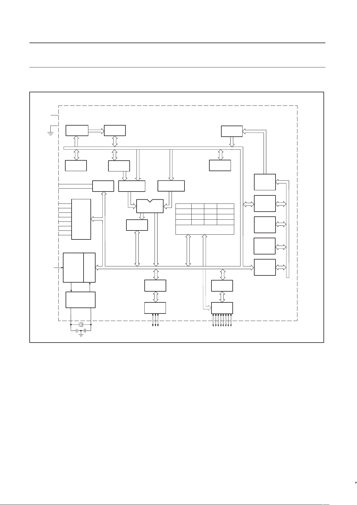
BLOCK DIAGRAM
RST
X1
X2
V
CC
V
SS
RAM
ROM/
EPROM
ACC
TMP2
TMP1
ALU
INSTRUCTION
REGISTER
PD
OSCILLATOR
PSW
BUFFER
DPTR
PCON TCON
IE
TH0 TL0
TH1 TL1
INTERRUPT, SERIAL
PORT AND TIMER BLOCKS
P1.0–P1.2
P3.0–P3.7
DAC
AV
SS
AV
CC
RAM ADDR
REGISTER
STACK
POINTER
PROGRAM
ADDRESS
REGISTER
PC
INCRE-
MENTER
PROGRAM
COUNTER
PORT 3
DRIVERS
PORT 1
DRIVERS
PORT 3
LATCH
PORT 1
LATCH
TIMING
AND
CONTROL
B
REGISTER
SU00666D
ANALOG
X
IN
XYZRAMP
DECOUPLE
VREG
XYDACBIAS
XYSOURCE
ZDAC
XYDAC
Page 4

Philips Semiconductors Preliminary specification
83C754/87C754
80C51 8-bit microcontroller family
4K/256 OTP/ROM, DAC, comparator, UART, reference
1998 Apr 23
4
PIN DESCRIPTION
MNEMONIC DIP
PIN NO.
TYPE NAME AND FUNCTION
V
SS
8 I Circuit Ground Potential.
V
CC
22 I Supply voltage during normal, idle, and power-down operation.
P1.0–P1.2 21, 23, 24 I/O Port 1: Port 1 is a 3-bit bidirectional I/O port with internal pull-ups on P1.0 and P1.1. Port 1 pins that
have 1s written to them can be used as inputs. As inputs, port 1 pins that are externally pulled low will
source current because of the internal pull-ups (P1.0, P1.1). (See DC Electrical Characteristics: I
IL
).
Port 1 also serves the special function features listed below (Note: P1.0 does not have the strong
pullup that is on for 2 oscillator periods.):
24 I INT0 (P1.0): External interrupt 0.
23 O CEX (P1.1): PCA clock output.
21 I VPP (P1.2): Programming voltage input (open drain).
P3.0–P3.7 1–4,
25–28
I/O Port 3: Port 3 is an 8-bit bidirectional I/O port with internal pull-ups. Port 3 pins that have 1s written to
them are pulled high by the internal pull-ups and can be used as inputs. As inputs, port 3 pins that are
externally being pulled low will source current because of the pull-ups. (See DC Electrical
Characteristics: I
IL
). Port 3 also functions as the data input for the EPROM memory location to be
programmed (or verified). (Note: P3.5 does not have the strong pullup that is on for 2 oscillator
periods.)
Port 3 also serves the special function as listed below:
3 I ECI (P3.6): External PCA clock input.
1 I RxD/T0 (P3.4): Serial port receiver data input.
Timer 0 external clock input.
4 I INT1: External interrupt 1.
2 I TxD/T1 (P3.5): Serial port transmitter data.
Timer 1 external clock input.
RST 5 I Reset: A high on this pin for two machine cycles while the oscillator is running resets the device. After
the device is reset, a 10-bit serial sequence, sent LSB first, applied to RESET, places the device in the
programming state allowing programming address, data and V
PP
to be applied for programming or
verification purposes. The RESET serial sequence must be synchronized with the X1 input. (Note: The
83/87C754 does not have an internal reset resistor.)
X1 7 I Crystal 1: Input to the inverting oscillator amplifier and input to the internal clock generator circuits. X1
also serves as the clock to strobe in a serial bit stream into RESET to place the device in the
programming state.
X2 6 O Crystal 2: Output from the inverting oscillator amplifier .
AV
CC
1
14 I Analog supply voltage and reference input.
AV
SS
1
13 I Analog supply and reference ground.
ZIN 9 I ZIN: Input to analog multiplexer.
YIN 10 I YIN: Input to analog multiplexer.
XIN 11 I XIN: Input to analog multiplexer.
XYZRAMP 12 O XYZRAMP: Provides a low impedance pulldown to VSS under S/W control.
DECOUPLE 15 O Decouple: Output from regulated supply for connection of decoupling capacitors.
VREG 16 O VREG: Provides regulated analog supply output.
XYDACBIAS 17 O XYDACBIAS: Provides source voltage for bias of external circuitry.
– Input which specifies verify mode (output enable) or the program mode.
/PGM = 1 output enabled (verify mode).
/PGM = 0 program mode.
XYSOURCE 18 O XYSOURCE: Provides source voltage from regulated analog supply.
ZDAC 19 O ZDAC: Switchable outp from the internal DAC.
ASEL (P0.0) – Input which indicates which bits of the EPROM address are applied to port 3.
ASEL = 0 low address byte available on port 3.
ASEL = 1 high address byte available on port 3 (only the three least significant bits are used).
XYDAC 20 O XYDAC: Non-switchable output from the internal DAC.
NOTE:
1. AV
SS
(reference ground) must be connected to 0V (ground). AVCC (reference input) cannot differ from VCC by more than ±0.2V, and must be
in the range 4.5V to 5.5V .
Page 5

Philips Semiconductors Preliminary specification
83C754/87C754
80C51 8-bit microcontroller family
4K/256 OTP/ROM, DAC, comparator, UART, reference
1998 Apr 23
5
OSCILLA T OR CHARACTERISTICS
X1 and X2 are the input and output, respectively, of an inverting
amplifier which can be configured for use as an on-chip oscillator.
To drive the device from an external clock source, X1 should be
driven while X2 is left unconnected. There are no requirements on
the duty cycle of the external clock signal, because the input to the
internal clock circuitry is through a divide-by-two flip-flop. However,
minimum and maximum high and low times specified in the data
sheet must be observed.
IDLE MODE
The 8XC754 includes the 80C51 power-down and idle mode
features. In idle mode, the CPU puts itself to sleep while all of the
on-chip peripherals stay active. The instruction to invoke the idle
mode is the last instruction executed in the normal operating mode
before the idle mode is activated. The CPU contents, the on-chip
RAM, and all of the special function registers remain intact during
this mode. The idle mode can be terminated either by any enabled
interrupt (at which time the process is picked up at the interrupt
service routine and continued), or by a hardware reset which starts
the processor in the same manner as a power-on reset. Upon
powering-up the circuit, or exiting from idle mode, sufficient time
must be allowed for stabilization of the internal analog reference
voltages before a D/A conversion is started.
Special Function Registers
The special function registers (directly addressable only) contain all
of the 8XC754 registers except the program counter and the four
register banks. Most of the special function registers are used to
control the on-chip peripheral hardware. Other registers include
arithmetic registers (ACC, B, PSW), stack pointer (SP) and data
pointer registers (DPH, DPL). Twelve of the SFRs are bit
addressable.
Data Pointer
The data pointer (DPTR) consists of a high byte (DPH) and a low
byte (DPL). In the 80C51 this register allows the access of external
data memory using the MOVX instruction. Since the 83C754 does
not support MOVX or external memory accesses, this register is
generally used as a 16-bit offset pointer of the accumulator in a
MOVC instruction. DPTR may also be manipulated as two
independent 8-bit registers.
POWER-DOWN MODE
In the power-down mode, the oscillator is stopped and the
instruction to invoke power-down is the last instruction executed.
Only the contents of the on-chip RAM are preserved. A hardware
reset is the only way to terminate the power-down mode. The control
bits for the reduced power modes are in the special function register
PCON.
Table 1. External Pin Status During Idle and
Power-Down Modes
MODE Port 1 Port 3
Idle Data Data
Power-down Data Data
ST ANDARD SERIAL INTERFACE
The serial port is full duplex, meaning it can transmit and receive
simultaneously. It is also receive-buffered, meaning it can
commence reception of a second byte before a previously received
byte has been read from the register. (However, if the first byte still
has not been read by the time reception of the second byte is
complete, one of the bytes will be lost.) The serial port receive and
transmit registers are both accessed at Special Function Register
SBUF. Writing to SBUF loads the transmit register, and reading
SBUF accesses a physically separate receive register.
The serial port can operate in 4 modes:
Mode 0: Serial data enters and exits through RxD. TxD outputs the
shift clock. 8 bits are transmitted/received (LSB first). The
baud rate is fixed at 1/12 the oscillator frequency.
Mode 1: 10 bits are transmitted (through TxD) or received (through
RxD): a start bit (0), 8 data bits (LSB first), and a stop bit
(1). On Receive, the stop bit goes into RB8 in Special
Function Register SCON. The baud rate is variable.
Mode 2: 11 bits are transmitted (through TxD) or received (through
RxD): a start bit (0), 8 data bits (LSB first), a
programmable 9th data bit, and a stop bit (1). On Transmit,
the 9th data bit (TB8 in SCON) can be assigned the value
of 0 or 1. Or, for example, the parity bit (P, in the PSW)
could be moved into TB8. On Receive, the 9th data bit
goes into RB8 in Special Function Register SCON, while
the stop bit is ignored. The baud rate is programmable to
either 1/32 or 1/64 the oscillator frequency.
Mode 3: 11 its are transmitted (through TxD) or received (through
RxD): a start bit (0), 8 data bits (LSB first), a
programmable 9th data bit, and a stop bit (1). In fact,
Mode 3 is the same as Mode 2 in all respects except baud
rate. the baud rate in Mode 3 is variable.
In all four modes, transmission is initiated by any instruction that
uses SBUF as a destination register. Reception is initiated in Mode 0
by the condition RI = 0 and REN = 1. Reception is initiated in the
other modes by the incoming start bit if REN = 1.
Multiprocessor Communications
Modes 2 and 2 have a special provision for multiprocessor
communications. In these modes, 9 data bits are received. The 9th
one goes into RB8. Then comes a stop bit. The port can be
programmed such that when the stop bit is received, the serial port
interrupt will be activated only if RB8 = 1. This feature is enabled by
setting bit SM2 in SCON. A way to use this feature in multiprocessor
systems is as follows:
When the master processor wants to transmit a block of data to one
of several slaves, it first sends out an address byte which identifies
the target slave. An address byte differs from a data byte in that the
9th bit is 1 in an address byte and 9 in a data byte. With SM2 = 1,
no slave will be interrupted by a data byte. An address byte,
however, will interrupt all slaves, so that each slave can examine the
received byte and see if it is being addressed. The addressed slave
will clear its SM2 bit and prepare to receive the data bytes that will
be coming. The slaves that were not being addressed leave their
SM2s set, and go on about their business, ignoring the coming data
bytes.
SM2 has no effect in Mode 0, and in Mode 1 can be used to check
the validity of the stop bit. In a Mode 1 reception, if SM2 = 1, the
receive interrupt will not be activated unless a valid stop bit is
received.
Page 6

Philips Semiconductors Preliminary specification
83C754/87C754
80C51 8-bit microcontroller family
4K/256 OTP/ROM, DAC, comparator, UART, reference
1998 Apr 23
6
Serial Port Control Register
The serial port control and status register is the Special Function
Register SCON, shown in Figure 1. This register contains not only
the mode selection bits, but also the 9th data bit for transmit and
receive (TB8 and RB8), and the serial port interrupt bits (TI and RI).
Baud Rates
The baud rate in Mode 0 is fixed: Mode 0 Baud Rate = Oscillator
Frequency / 12. The baud rate in Mode 2 depends on the value of
bit SMOD in Special function Register PCON. If SMOD = 0 (which is
the value on reset), the baud rate is 1/64 the oscillator frequency.
If SMOD = 1, the baud rate is 1/32 the oscillator frequency.
Mode 2 Baud Rate
2
SMOD
64
(Oscillator Frequency)
In the 8XC754, the baud rates in Modes 1 and 3 are determined by
the Timer 1 overflow rate.
Using Timer 1 to Generate Baud Rates
When Timer 1 is used as the baud rate generator, the baud rates in
Modes 1 and 3 are determined by the Timer 1 overflow rate and the
value of SMOD as follows:
Mode 1, 3 Baud Rate
2
SMOD
32
(Timer 1 Overflow Rate)
The Timer 1 interrupt should be disabled in this application. The
Timer itself can be configured for either “timer” or “counter”
operation, and in any of its 3 running modes. In the most typical
applications, it is configured for “timer” operation, in the auto-reload
mode (high nibble of TMOD = 0010B). In that case the baud rate is
given by the formula:
Mode 1, 3 Baud Rate
2
SMOD
32
Oscillator Frequency
12 [256 (TH1)]
One can achieve very low baud rates with Timer 1 by leaving the
Timer 1 interrupt enabled, and configuring the Timer to run as a
16-bit timer (high nibble of TMOD = 0001B), and using the Timer 1
interrupt to do a 16-bit software reload. Figure 2 lists various
commonly used baud rates and how they can be obtained from
Timer 1.
SM2 Enables the multiprocessor communication feature in Modes 2 and 3. In Mode 2 or 3, if SM2 is set to 1, then Rl will not be
activated if the received 9th data bit (RB8) is 0. In Mode 1, if SM2=1 then RI will not be activated if a valid stop bit was not
received. In Mode 0, SM2 should be 0.
REN Enables serial reception. Set by software to enable reception. Clear by software to disable reception.
TB8 The 9th data bit that will be transmitted in Modes 2 and 3. Set or clear by software as desired.
RB8 In Modes 2 and 3, is the 9th data bit that was received. In Mode 1, it SM2=0, RB8 is the stop bit that was received. In Mode 0,
RB8 is not used.
TI Transmit interrupt flag. Set by hardware at the end of the 8th bit time in Mode 0, or at the beginning of the stop bit in the other
modes, in any serial transmission. Must be cleared by software.
RI Receive interrupt flag. Set by hardware at the end of the 8th bit time in Mode 0, or halfway through the stop bit time in the other
modes, in any serial reception (except see SM2). Must be cleared by software.
MSB
LSB
SM0 SM1 SM2 REN TB8 RB8 TI RI
Where SM0, SM1 specify the serial port mode, as follows:
SM0 SM1 Mode Description Baud Rate
0 0 0 shift register f
OSC
/ 12
0 1 1 8-bit UART variable
1 0 2 9-bit UART f
OSC
/64 or f
OSC
/32
1 1 3 9-bit UART variable
SU00120
Figure 1.
Timer 1
Baud Rate
f
OSC
SMOD
C/T Mode Reload Value
Mode 0 Max: 1.67MHz 20MHz X X X X
Mode 2 Max: 625k 20MHz 1 X X X
Mode 1, 3 Max: 104.2k 20MHz 1 0 2 FFH
19.2k 11.059MHz 1 0 2 FDH
9.6k 11.059MHz 0 0 2 FDH
4.8k 11.059MHz 0 0 2 FAH
2.4k 11.059MHz 0 0 2 F4H
1.2k 11.059MHz 0 0 2 E8H
137.5 11.986MHz 0 0 2 1DH
110 6MHz 0 0 2 72H
110 12MHz 0 0 1 FEEBH
Figure 2. Timer 1 Generated Commonly Used Baud Rates
Page 7

Philips Semiconductors Preliminary specification
83C754/87C754
80C51 8-bit microcontroller family
4K/256 OTP/ROM, DAC, comparator, UART, reference
1998 Apr 23
7
DIFFERENCES BETWEEN THE 8XC754 AND THE
80C51
Program Memory
On the 8XC754, program memory is 4096 bytes long and is not
externally expandable, so the 80C51 instructions MOVX, LJMP, and
LCALL are not implemented. If these instructions are executed, the
appropriate number of instruction cycles will take place along with
external fetches; however, no operation will take place. The LJMP
may not respond to all program address bits. The only fixed
locations in program memory are the addresses at which execution
is taken up in response to reset and interrupts, which are as follows:
Program Memory
Event Address
Reset 000
External INT0
003
Timer 0 00B
External INT1
013
PCA 01B
SIO/TF1 023
Memory Organization
The 8XC754 manipulates operands in three memory address
spaces. The first is the program memory space which contains
program instructions as well as constants such as look-up tables.
The program memory space contains 4k bytes in the 8XC754.
The second memory space is the data memory array which has a
logical address space of 256 bytes.
The third memory space is the special function register array having
a 128-byte address space (80H to FFH). Only selected locations in
this memory space are used (see Table 2). Note that the
architecture of these memory spaces (internal program memory,
internal data memory , and special function registers) is identical to
the 80C51, and the 8XC754 varies only in the amount of memory
physically implemented.
The 8XC754 does not directly address any external data or program
memory spaces. For this reason, the MOVX instructions in the
80C51 instruction set are not implemented in the 83C754, nor are
the alternate I/O pin functions RD
and WR.
I/O Ports
The I/O pins provided by the 8XC754 consist of port 1 and port 3.
Port 1
Port 1 is a 3-bit bidirectional I/O port and includes alternate functions
on some pins of this port. P1.1 is provided with internal pullups while
the remaining pins (P1.0 and P1.2) are an open drain output
structure. The alternate functions for port 1 are:
INT0 – External interrupt 0.
PCAOUT – PCA clock output
V
PP
– External programming voltage.
Port 3
Port 3 is an 8-bit bidirectional I/O port structure. P3.5 is open drain.
The alternate functions for port 3 are:
RxD – Serial port receiver data input.
T1 – Timer 1 external clock input.
INT1
– External interrupt 1.
TxD – Serial port transmitter data.
T0 – Timer 0 external clock input.
ECI – PCA external clock input.
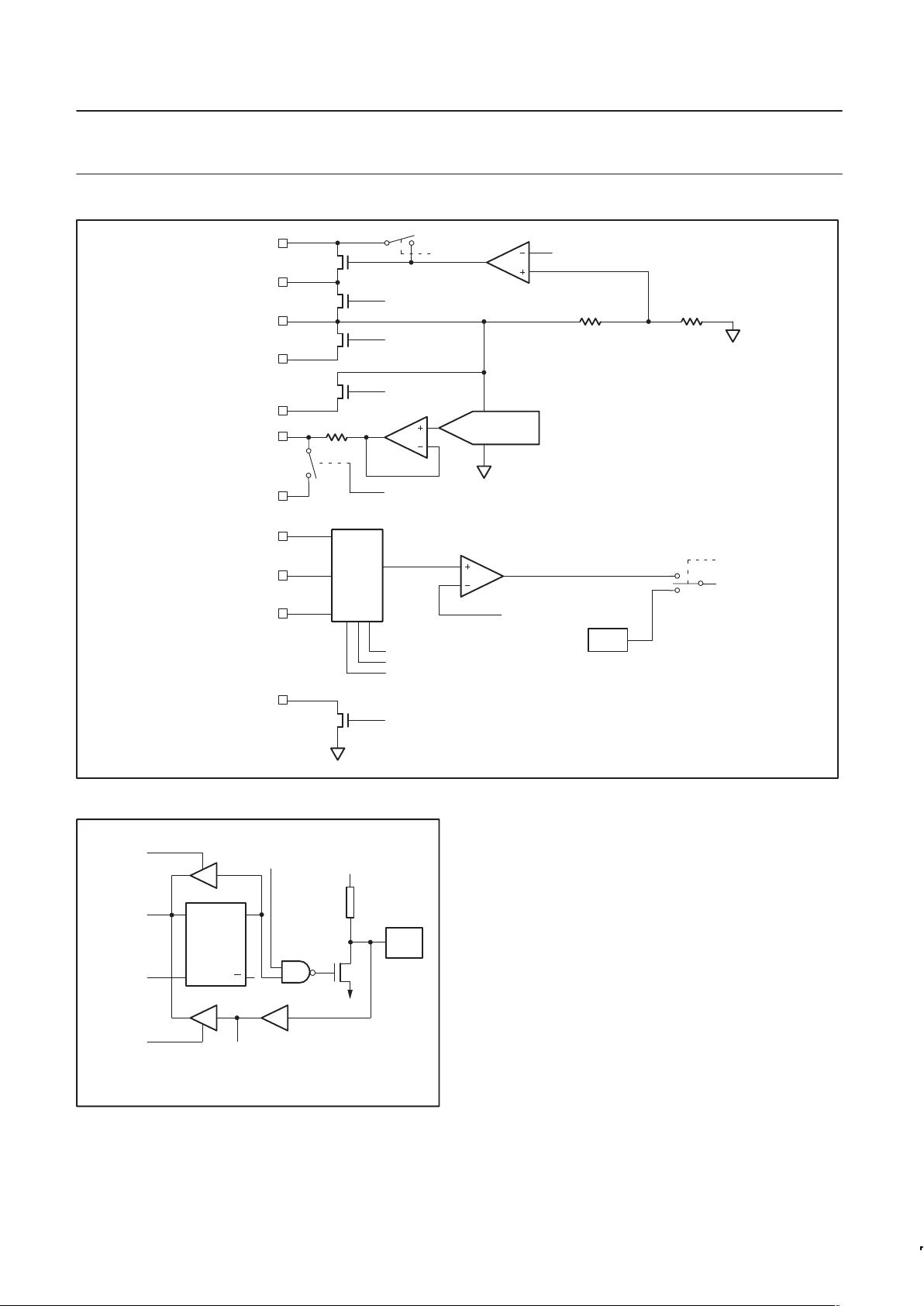
Analog Section
The analog section of the 8XC754, shown in Figure 3, consists of
four major elements: a bandgap referenced voltage regulator, an
8-bit DAC, an input multiplexer and comparator, and a low
impedance pulldown device.
The bandgap voltage regulator uses the AV
CC
pin as its supply and
produces a regulated output on the VREG pin. The bandgap
reference is enabled/disabled by AC0. The regulator also supplies
the analog supply voltage for the DAC. The regulator may be
switched on/off by means of the AC1 bit in the analog control
register (ACON0). The regulator output may also be supplied to the
XYDACBIAS and XYSOURCE pins by means of bits AC3 and AC4,
respectively. The DECOUPLE pin is provided for decoupling the
regulator output.
The DAC is an 8-bit device and its output appears on the XYDAC
pin. In addition, the DAC output may also be routed to the ZDAC pin
by means of bit AC6 in the ACON0 register. The DAC output is not
buffered, so external load impedances should be taken into
consideration when using either of these outputs.
A 3-input multiplexer is provided, whose output is connected to the
positive reference of a comparator. The multiplexer output is
controlled by bits MUX2:0 of ACON1. A bandgap reference supplies
the negative reference of the comparator. The output of the
comparator may be used the trigger the capture input of PCA
module.
A low impedance pulldown is supplied at the XYZRAMP pin and is
controlled by bit AC5 of ACON0.
Interrupt Subsystem—Fixed Priority
The interrupt structure is a seven-source, two-level interrupt system.
Simultaneous interrupt conditions are resolved by a single-level,
fixed priority as follows:
Highest priority:
Pin INT0
Timer flag 0
Lowest priority:
Pin INT1
PCA
Serial I/O – TF1
The vector addresses are as follows:
Source Vector Address
INT0 0003H
TF0 000BH
INT1 0013H
PCA 001BH
SIO/TF1 0023H
Interrupt Enable Register
MSB LSB
EA
– – ES/T1 EC EX1 ET0 EX0
Position Symbol Function
IE.7 EA Global interrupt disable when EA = 0
IE.6 –
IE.5 –
IE.4 ES/T1 Serial port/Timer Flag 1
IE.3 EC PCA interrupt
IE.2 EX1 External interrupt 1
IE.1 ET0 Timer 0 overflow
IE.0 EX0 External interrupt 0
Page 8
Philips Semiconductors Preliminary specification
83C754/87C754
80C51 8-bit microcontroller family
4K/256 OTP/ROM, DAC, comparator, UART, reference
1998 Apr 23
8
AV
CC
DECOUPLE
VREG
BANDGAP REF*
AC2
XYDACBIAS
20K 10K
XYSOURCE
XYDAC
AC4
AC3
ZDAC
1K
AC6
ANALOG
MUX
ZIN
YIN
XIN
MUX0
MUX1
TO PCA TRIGGER
BANDGAP REF
XYZRAMP
AC5
SU00765A
AC1
*ENABLED/DISABLED BY AC0
EXT
AC7
MUX2
DCON 7:0 (84H)
Figure 3. Analog Section
LATCH
DQ
CL Q
READ
LATCH
INT. BUS
WRITE TO
LATCH
READ
PIN
ALTERNATE INPUT
FUNCTION
V
DD
PIN
INTERNAL*
PULL-UP
ALTERNATE
OUTPUT
FUNCTION
SU00671
*PINS LISTED AS OPEN DRAIN WILL NOT HAVE THIS PULLUP
Figure 4. Typical Port Bit Latches and I/O Buffers
Page 9

Philips Semiconductors Preliminary specification
83C754/87C754
80C51 8-bit microcontroller family
4K/256 OTP/ROM, DAC, comparator, UART, reference
1998 Apr 23
9
Table 2. 8XC754 Special Function Registers
SYMBOL DESCRIPTION
DIRECT
ADDRESS
BIT ADDRESS, SYMBOL, OR ALTERNATIVE PORT FUNCTION
MSB LSB
RESET
VALUE
ACC* Accumulator E0H E7 E6 E5 E4 E3 E2 E1 E0 00H
ACON0* Analog Control 0 A0H AC7 AC6 AC5 AC4 AC3 AC2 AC1 AC0
ACON1* Analog Control 1 C0H – – – – TSI MUX2 MUX1 MUX0
B* B register F0H F7 F6 F5 F4 F3 F2 F1 F0 00H
CCAPH# PCA Module
Capture High
FEH
CCAPL# PCA Module
Capture Low
EEH
CCAPM# PCA Module Mode DEH – ECOM CAPP CAPN MAT TOG PWM ECCF x0000000B
DF DE DD DC DB DA D9 D8
CCON*#
PCA Counter
Control
D8H CF CR – CCF4 – – – – 00x00000B
CH# PCA Counter High F9H 00H
CL# PCA Counter Low E9H 00H
CMOD# PCA Counter Mode D9H CODL WDTE – – – CPS1 CPS0 ECF 00xxx000B
DCON DAC Control 84H
DPTR:
DPL
DPH
Data pointer
(2 bytes)
Data pointer low
Data pointer high
82H
83H
00H
00H
AF AE AD AC AB AA A9 A8
IE*# Interrupt Enable A8H EA – – ES/T1 EC EX1 ET0 EX0 00H
AF AE AD AC AB AA A9 A8
IP* Interrupt Priority B8H – – – PS/T1 PPC PX1 PT0 PX0 x0000000B
– – – 84 83 82 81 80 xxx11111B
P1*# Port 1 90H – – – – – ZIN
XYZRAMP
XYSOURCE
P3*# Port 3 B0H INT1 ECI TxD RxD – – – –
PCON Power control 87H
SMOD1 SMOD0
– POF GF1 GF0 PD IDL 00xxxx00B
D7 D6 D5 D4 D3 D2 D1 D0
PSW* Program status word D0H CY AC F0 RS1 RS0 OV – P 00H
SBUF Serial Data Buffer 99H xxxxxxxxB
SP Stack pointer 81H 07H
9F 9E 9D 9C 9B 9A 99 98
SCON* Serial Control 98H SM0 SM1 SM2 REN TB8 RB8 TI RI 00H
8F 8E 8D 8C 8B 8A 89 88
TCON* Timer Control 88H TF1 TR1 TF0 TR0 IE1 IT1 IE0 IT0 00H
TH0 Timer High 0 8CH 00H
TH1 Timer High 1 8DH 00H
TL0 Timer Low 0 8AH 00H
TL1 Timer Low 1 8BH 00H
TMOD Timer Mode 89H GATE C/T M1 M0 GATE C/T M1 M0 00H
C7 C6 C5 C4 C3 C2 C1 C0
* SFRs are bit addressable.
# SFRs are modified from or added to the 80C51 SFRs.
Page 10

Philips Semiconductors Preliminary specification
83C754/87C754
80C51 8-bit microcontroller family
4K/256 OTP/ROM, DAC, comparator, UART, reference
1998 Apr 23
10
COUNTER/TIMER
The 8XC754 counter/timers are designated Timer 0 and 1. They are
identical to the 80C51 counter/timers. (Timer 1 shares its interrupt
with the serial port.)
Programmable Counter Array (PCA)
The Programmable Counter Array is a special Timer that has one
16-bit capture/compare module associated with it. The module can
be programmed to operate in one of four modes: rising and/or falling
edge capture, software timer, high-speed output, or pulse width
modulator. The basic PCA configuration is shown in Figure 5.
The PCA timer can be programmed to run at: 1/12 the oscillator
frequency, 1/4 the oscillator frequency, the Timer 0 overflow, or the
input on the ECI pin (P3.1). The timer count source is determined
from the CPS1 and CPS0 bits in the CMOD SFR as follows (see
Figure 8):
CPS1 CPS0 PCA Timer Count Source
0 0 1/12 oscillator frequency
0 1 1/4 oscillator frequency
1 0 Timer 0 overflow
1 1 External Input at ECI pin
In the CMOD SFR are three additional bits associated with the PCA.
They are CIDL which allows the PCA to stop during idle mode,
WDTE which enables or disables the watchdog function, and ECF
which when set causes an interrupt and the PCA overflow flag, CF
(in the CCON SFR) to be set when the PCA timer overflows. These
functions are shown in Figure 6.
The watchdog timer function is implemented in module 4 as
implemented in other parts that have a PCA that are available on the
market.
The CCON SFR contains the run control bit for the PCA and the
flags for the PCA timer (CF) and module (refer to Figure 9). To run
the PCA the CR bit (CCON.6) must be set by software. The PCA is
shut off by clearing this bit. The CF bit (CCON.7) is set when the
PCA counter overflows and an interrupt will be generated if the ECF
bit in the CMOD register is set, The CF bit can only be cleared by
software. Bit 4 of the CCON register is the flag for the module and is
set by hardware when either a match or a capture occurs. This flag
can only be cleared by software. The PCA interrupt system shown in
Figure 7.
The CCAPM register contains the bits that control the mode in which
the module will operate. The ECCF bit enables the CCF flag in the
CCON SFR to generate an interrupt when a match or compare
occurs in the associated module. PWM (CCAPM.1) enables the
pulse width modulation mode. The TOG bit (CCAPM.2) when set
causes the CEX output associated with the module to toggle when
there is a match between the PCA counter and the module’s
capture/compare register . The match bit MAT (CCAPM.3), when set,
will cause the CCF bit in the CCON register to be set when there is
a match between the PCA counter and the module’s
capture/compare register.
The next two bits CAPN (CCAPM.4) and CAPP (CCAPM.5)
determine the edge that a capture input will be active on. The CAPN
bit enables the negative edge, and the CAPP bit enables the
positive edge. If both bits are set both edges will be enabled and a
capture will occur for either transition. The last bit in the register
ECOM (CCAPM.6) when set enables the comparator function.
Figure 11 shows the CCAPM settings for the various PCA functions.
There are two additional registers associated with the PCA module.
They are CCAPH and CCAPL and these are the registers that store
the 16-bit count when a capture occurs or a compare should occur.
When the module is used in the PWM mode these registers are
used to control the duty cycle of the output.
PCA Capture Mode
To use the PCA module in the capture mode, either one or both of
the CCAPM bits CAPN and CAPP must be set. The external CEX
input for the module is sampled for transition. When a valid transition
occurs, the PCA hardware loads the value of the PCA counter
registers (CH and CL) into the module’s capture registers (CCAPL
and CCAPH). If the CCF bit for the module in the CCON SFR and
the ECCF bit in the CCAPM SFR are set, then an interrupt will be
generated. Refer to Figure 12.
16-bit Software Timer Mode
The PCA modules can be used as software timers by setting both
the ECOM and MAT bits in the module’ s CCAPM register. The PCA
timer will be compared to the module’s capture registers and when a
match occurs an interrupt will occur if the CCF (CCON SFR) and the
ECCF (CCAPM SFR) bits for the module are both set (see
Figure 13).
High Speed Output Mode
In this mode the CEX output associated with the PCA module will
toggle each time a match occurs between the PCA counter and the
module’s capture registers. To activate this mode the TOG, MAT,
and ECOM bits in the module’s CCAPM SFR must be set (see
Figure 14).
Pulse Width Modulator Mode
The PCA module can be used as a PWM output. Figure 15 shows
the PWM function. The frequency of the output depends on the
source for the PCA timer. The duty cycle of the module is
independently variable using the module’s capture register CCAPL.
When the value of the PCA CL SFR is less than the value in the
module’s CCAPL SFR, the output will be low, when it is equal to or
greater than the output will be high. When CL overflows from FF to
00, CCAPL is reloaded with the value in CCAPH. This allows
updating the PWM without glitches. The PWM and ECOM bits in the
module’s CCAPM register must be set to enable the PWM mode.
MODULE FUNCTIONS:
16-BIT CAPTURE
16-BIT TIMER
16-BIT HIGH SPEED OUTPUT
8-BIT PWM
WATCHDOG TIMER
PCA MODULE
P1.1/CEX
16 BITS
PCA TIMER/COUNTER
TIME BASE FOR PCA MODULES
16 BITS
SU00672B
Figure 5. Programmable Counter Array (PCA)
Page 11

Philips Semiconductors Preliminary specification
83C754/87C754
80C51 8-bit microcontroller family
4K/256 OTP/ROM, DAC, comparator, UART, reference
1998 Apr 23
11
CF CR CCF –– –– –– ––––
CCON
(D8H)
CH CL
OVERFLOW
INTERRUPT
16–BIT UP COUNTER
IDLE
TO PCA
MODULES
CMOD
(D9H)
CIDL WDTE –– –– –– CPS1 CPS0 ECF
OSC/12
OSC/4
TIMER 0
OVERFLOW
EXTERNAL INPUT
(P3.6/ECI)
DECODE
00
01
10
11
SU00673B
Figure 6. PCA Timer/Counter
PCA MODULE
PCA TIMER/COUNTER
CF CR CCF –– –– –– ––––
CMOD.0 ECF
CCAPM
TO
INTERRUPT
PRIORITY
DECODER
CCON
(D8H)
IE.6
EC
IE.7
EA
SU00674A
ECCFn
Figure 7. PCA Interrupt System
Page 12

Philips Semiconductors Preliminary specification
83C754/87C754
80C51 8-bit microcontroller family
4K/256 OTP/ROM, DAC, comparator, UART, reference
1998 Apr 23
12
CMOD Address = OD9H
Reset Value = 00XX X000B
CIDL WDTE – – – CPS1 CPS0 ECF
Bit Addressable
Bit:
Symbol Function
CIDL Counter Idle control: CIDL = 0 programs the PCA Counter to continue functioning during idle Mode. CIDL = 1 programs
it to be gated off during idle.
WDTE Watchdog Timer Enable: WDTE = 0 disables W atchdog Timer function on PCA Module. WDTE = 1 enables it.
– Not implemented, reserved for future use.*
CPS1 PCA Count Pulse Select bit 1.
CPS0 PCA Count Pulse Select bit 0.
CPS1 CPS0 Selected PCA Input**
0 0 0 Internal clock, f
OSC
÷ 12
0 1 1 Internal clock, f
OSC
÷ 4
1 0 2 Timer 0 overflow
1 1 3 External clock at ECI/P3.1 pin (max. rate = f
OSC
÷ 8)
ECF PCA Enable Counter Overflow interrupt: ECF = 1 enables CF bit in CCON to generate an interrupt. ECF = 0 disables
that function of CF.
NOTE:
* User software should not write 1s to reserved bits. These bits may be used in future 8051 family products to invoke new features. In that case, the reset or inactive value of the
new bit will be 0, and its active value will be 1. The value read from a reserved bit is indeterminate.
** f
OSC
= oscillator frequency
SU00675A
76543210
Figure 8. CMOD: PCA Counter Mode Register
CCON Address = OD8H
Reset Value = 00X0 0000B
CF CR –– CCF –– –– –– ––
Bit Addressable
Bit:
Symbol Function
CF PCA Counter Overflow flag. Set by hardware when the counter rolls over. CF flags an interrupt if bit ECF in CMOD is
set. CF may be set by either hardware or software but can only be cleared by software.
CR PCA Counter Run control bit. Set by software to turn the PCA counter on. Must be cleared by software to turn the PCA
counter off.
– Not implemented, reserved for future use*.
CCF PCA Module interrupt flag. Set by hardware when a match or capture occurs. Must be cleared by software.
NOTE:
* User software should not write 1s to reserved bits. These bits may be used in future 8051 family products to invoke new features. In that case, the reset or inactive value of the
new bit will be 0, and its active value will be 1. The value read from a reserved bit is indeterminate.
SU00676A
76543210
Figure 9. CCON: PCA Counter Control Register
Page 13

Philips Semiconductors Preliminary specification
83C754/87C754
80C51 8-bit microcontroller family
4K/256 OTP/ROM, DAC, comparator, UART, reference
1998 Apr 23
13
CCAPMn Address CCAPM 0DEH
Reset Value = X000 0000B
–– ECOM CAPP CAPN MAT TOG PWM ECCF
Not Bit Addressable
Bit:
Symbol Function
– Not implemented, reserved for future use*.
ECOM Enable Comparator. ECOM = 1 enables the comparator function.
CAPP Capture Positive, CAPP = 1 enables positive edge capture.
CAPN Capture Negative, CAPN = 1 enables negative edge capture.
MAT Match. When MAT = 1, a match of the PCA counter with this module’s compare/capture register causes the CCF bit in
CCON to be set, flagging an interrupt.
TOG Toggle. When TOG = 1, a match of the PCA counter with this module’s compare/capture register causes the CEX pin
to toggle.
PWM Pulse Width Modulation Mode. PWM4 = 1 enables the CEX pin to be used as a pulse width modulated output.
ECCF Enable CCF interrupt. Enables compare/capture flag CCF in the CCON register to generate an interrupt.
NOTE:
*User software should not write 1s to reserved bits. These bits may be used in future 8051 family products to invoke new features. In that case, the reset or inactive value of the new
bit will be 0, and its active value will be 1. The value read from a reserved bit is indeterminate.
SU00677A
76543210
Figure 10. CCAPM: PCA Modules Compare/Capture Registers
– ECOM CAPP CAPN MAT TOG PWM ECCF MODULE FUNCTION
X 0 0 0 0 0 0 0 No operation
X X 1 0 0 0 0 X 16-bit capture by a positive-edge trigger on CEX
X X 0 1 0 0 0 X 16-bit capture by a negative trigger on CEX
X X 1 1 0 0 0 X 16-bit capture by a transition on CEX
X 1 0 0 1 0 0 X 16-bit Software Timer
X 1 0 0 1 1 0 X 16-bit High Speed Output
X 1 0 0 0 0 1 0 8-bit PWM
X 1 0 0 1 X 0 X Watchdog Timer
Figure 11. PCA Module Modes (CCAPM Register)
CF CR CCF ––––
CCON
(D8H)
–– ECOM CAPP CAPN MAT TOG PWM ECCF
CCAPM
CH CL
CCAPH CCAPL
CEX
CAPTURE
PCA INTERRUPT
PCA TIMER/COUNTER
0 000
(TO CCF)
SU00678A
––––––
Figure 12. PCA Capture Mode
Page 14

Philips Semiconductors Preliminary specification
83C754/87C754
80C51 8-bit microcontroller family
4K/256 OTP/ROM, DAC, comparator, UART, reference
1998 Apr 23
14
MATCH
CF CR CCF –– –– –– ––––
CCON
(D8H)
–– ECOM CAPP CAPN MAT TOG PWM ECCF
CCAPM
CH CL
CCAPH
CCAPL
PCA INTERRUPT
PCA TIMER/COUNTER
0000
16–BIT COMPARATOR
(TO CCF)
ENABLE
WRITE TO
CCAPH
RESET
WRITE TO
CCAPL
01
SU00679A
Figure 13. PCA Compare Mode
CF CR CCF –– –– –– ––––
CCON
(D8H)
–– ECOM CAPP CAPN MAT TOG PWM ECCF
CCAPM
CH CL
CCAPH CCAPL
PCA INTERRUPT
PCA TIMER/COUNTER
1000
16–BIT COMPARATOR
(TO CCF4)
WRITE TO
CCAPH
RESET
WRITE TO
CCAPL
01
ENABLE
CEX
TOGGLE
MATCH
SU00680A
Figure 14. PCA High Speed Output Mode
Page 15

Philips Semiconductors Preliminary specification
83C754/87C754
80C51 8-bit microcontroller family
4K/256 OTP/ROM, DAC, comparator, UART, reference
1998 Apr 23
15
CL < CCAPL
–– ECOM CAPP CAPN MAT TOG PWM ECCF CCAPM
PCA TIMER/COUNTER
0000
CL
CCAPL
CEX
8–BIT
COMPARATOR
OVERFLOW
CCAPH
ENABLE
0
1
CL >= CCAPL
0
SU00681A
Figure 15. PCA PWM Mode
–– ECOM CAPP CAPN MAT TOG PWM ECCF
CCAPM
(DEH)
CH CL
CCAPH CCAPL
RESET
PCA TIMER/COUNTER
X000
16–BIT COMPARATOR
MATCH
ENABLE
WRITE TO
CCAPH
RESET
WRITE TO
CCAPL
01
1
CMOD
(D9H)
CIDL WDTE –– –– –– CPS1 CPS0 ECF
X
SU00682A
Figure 16. PCA Watchdog Timer
Page 16

Philips Semiconductors Preliminary specification
83C754/87C754
80C51 8-bit microcontroller family
4K/256 OTP/ROM, DAC, comparator, UART, reference
1998 Apr 23
16
ABSOLUTE MAXIMUM RATINGS
1, 3, 4
PARAMETER
RATING UNIT
Storage temperature range –65 to +150 °C
Voltage from V
CC
to V
SS
–0.5 to +6.5 V
Voltage from any pin to VSS (except VPP) –0.5 to VCC + 0.5 V
Power dissipation 1.0 W
Voltage from VPP pin to V
SS
–0.5 to + 13.0 V
DC ELECTRICAL CHARACTERISTICS
T
amb
= 0°C to +70°C, AVCC = 5V ±5, AVSS = 0V
4
VCC = 5V ± 10%, VSS = 0V
LIMITS
4
SYMBOL
PARAMETER
TEST CONDITIONS
MIN TYP
1
MAX
UNIT
I
CC
Supply current (see Figure 19)
Inputs
V
IL
Input low voltage, port 1, 3 –0.5
0.2VCC–0.1
V
V
IH
Input high voltage, port 1, 3 0.2VCC+0.9 VCC+0.5 V
V
IH1
Input high voltage, X1, RST 0.7V
CC
VCC+0.5 V
Outputs
V
OL
Output low voltage, port 3 IOL = 1.6mA
2
0.45 V
V
OL1
Output low voltage, port 1.0, 1.1, 1.2 IOL = 3.2mA
2
0.45 V
V
OH
Output high voltage, ports 3, 1.0, 1.1 IOH = –60µA, 2.4 V
I
LI
Input leakage current, port 1, 3, RST 0.45 < VIN < V
CC
+10 µA
I
IL
Logical 0 input cirrent, ports 1 and 3 VIN = 0.45V –50 µA
C
IO
Pin capacitance T est freq = 1MHz,
T
amb
= 25°C
10 pF
I
PD
Power-down current
5
VCC = 2 to 5.5V
VCC = 2 to 6.0V
(83C754)
50 µA
V
PP
VPP program voltage (87C754 only) VSS = 0V
VCC = 5V±10%
T
amb
= 21°C to 27°C
12.5 13.0 V
I
PP
Program current (87C754 only) VPP = 13.0V 50 mA
NOTES:
1. Stresses above those listed under Absolute Maximum Ratings may cause permanent damage to the device. This is a stress rating only and
functional operation of the device at these or any conditions other than those described in the AC and DC Electrical Characteristics section
of this specification is not implied.
2. Under steady state (non-transient) conditions, IOL must be externally limited as follows:
Maximum I
OL
per port pin: 10mA
Maximum I
OL
per 8-bit port: 26mA
Maximum total I
OL
for all outputs: 67mA
If I
OL
exceeds the test condition, VOL may exceed the related specification. Pins are not guaranteed to sink current greater than the listed
test conditions.
3. This product includes circuitry specifically designed for the protection of its internal devices from the damaging effects of excessive static
charge. Nonetheless, it is suggested that conventional precautions be taken to avoid applying greater than the rated maxima.
4. Parameters are valid over operating temperature range unless otherwise specified. All voltages are with respect to V
SS
unless otherwise
noted.
5. Power-down I
CC
is measured with all output pins disconnected; port 0 = VCC; X2, X1 n.c.; RST = VSS.
6. I
CC
is measured with all output pins disconnected; X1 driven with t
CLCH
, t
CHCL
= 5ns, VIL = VSS + 0.5V, VIH = VCC – 0.5V; X2 n.c.;
RST = port 0 = V
CC
. ICC will be slightly higher if a crystal oscillator is used.
7. Idle I
CC
is measured with all output pins disconnected; X1 driven with t
CLCH
, t
CHCL
= 5ns, VIL = VSS + 0.5V, VIH = VCC – 0.5V; X2 n.c.;
port 0 = V
CC
; RST = VSS.
8. Load capacitance for ports = 80pF.
Page 17

Philips Semiconductors Preliminary specification
83C754/87C754
80C51 8-bit microcontroller family
4K/256 OTP/ROM, DAC, comparator, UART, reference
1998 Apr 23
17
ANALOG SECTION ELECTRICAL CHARACTERISTICS
T
amb
= 0°C to +70°C, AVCC = 5V ±5, AVSS = 0V
4
VCC = 5V ± 10%, VSS = 0V
LIMITS
4
SYMBOL
PARAMETER
TEST CONDITIONS
MIN TYP
1
MAX
UNIT
Analog Inputs (D/A guaranteed only with quartz window covered.)
AV
CC
Analog supply voltage 4.5 – 5.5 V
Sensor resistor 330 – 3K Ω
IAV
CC
AC0 = 0 IC only – 0.88 1.5 mA
AC0 = 1 – – 10 µA
Regulator
VREG 3.6 3.8 4.0 V
IVREG 13 – 55 mA
CDECOUPLE Stability requirement 3 10 – µF
RDSONQ1 – 7 – Ω
ILEAKAGEQ1 – TBD – µA
ILEAKAGEQ2 – TBD – µA
PSRR 100Hz – –40 – dB
VREGREJ VREG rejection of 1 Volt A VCC step change –100 – 100 mV
TVREG VREG turn on time Q1 off, 330Ω sensor – 2 5 ms
MUX and Comparator
Comparator trip point 1.14 1.26 1.38 V
Comparator delay input 0.04V/µs – 50 – ns
Comparator delay change AVCC 4.5 to 5.5V –10 2 10 ns
MUX impedance – 1 – kΩ
ILEAKAGEMUX – TBD – µA
Digital-to-Analog Conversion
ZDAC, XYDAC monotonicity 0 – – bits
ZDAC, XYDAC impedance – 10 – kΩ
DAC selection switch impedance – 40 – Ω
DAC settling – 1 – µs
ZDAC switch impedance – 50 – Ω
ZDAC switch impedance change AVCC 4.5 to 5.5V –20 – 20 Ω
ZDAC switch leakage – TBD – µA
Switches
XYZRAMP impedance – 25 100 Ω
XYZRAMP impedance change AVCC 4.5 to 5.5V –25 – 25 Ω
XYZRAMP leakage – TBD – µA
XYZRAMP discharge to 1LSB (1.6mV) – 1.5 10 µs
XYZRAMP delay turn on time – 6 50 ns
XYZRAMP start time change AVCC 4.5 to 5.5V –10 – 10 ns
XYDACBIAS impedance – 7 13 Ω
XYDACBIAS leakage – TBD – µA
XYDACBIAS switching time – 130 1000 ns
XYSOURCE impedance – 150 300 Ω
XYSOURCE impedance change AVCC 4.5 to 5.5V –100 – 100 Ω
XYSOURCE leakage – TBD – µA
XYSOURCE switching time – 30 500 ns
Page 18

Philips Semiconductors Preliminary specification
83C754/87C754
80C51 8-bit microcontroller family
4K/256 OTP/ROM, DAC, comparator, UART, reference
1998 Apr 23
18
AC ELECTRICAL CHARACTERISTICS
T
amb
= 0°C to +70°C, VCC = 5V ±10%, VSS = 0V
4, 8
16MHz CLOCK VARIABLE CLOCK
SYMBOL PARAMETER MIN MAX MIN MAX UNIT
1/t
CLCL
Oscillator frequency 3.5 16 MHz
External Clock (Figure 17)
t
CHCX
High time 20 20 ns
t
CLCX
Low time 20 20 ns
t
CLCH
Rise time 20 20 ns
t
CHCL
Fall time 20 20 ns
EXPLANATION OF THE AC SYMBOLS
Each timing symbol has five characters. The first character is always
‘t’ (= time). The other characters, depending on their positions,
indicate the name of a signal or the logical status of that signal.
The designations are:
C – Clock
D – Input data
H – Logic level high
L – Logic level low
Q – Output data
T – Time
V – Valid
X – No longer a valid logic level
Z – Float
t
CHCL
t
CLCL
t
CLCH
t
CHCX
VCC –0.5
0.45V
0.2 V
CC
+ 0.9
0.2 V
CC
– 0.1
t
CLCX
SU00297
Figure 17. External Clock Drive
0.2 VCC + 0.9
0.2 VCC – 0.1
V
CC
–0.5
0.45V
SU00307
Figure 18. AC Testing Input/Output
Page 19

Philips Semiconductors Preliminary specification
83C754/87C754
80C51 8-bit microcontroller family
4K/256 OTP/ROM, DAC, comparator, UART, reference
1998 Apr 23
19
4MHz 8MHz 12MHz 16MHz
FREQ
MAX ACTIVE I
CC
6
TYP ACTIVE I
CC
6
MAX IDLE I
CC
7
TYP IDLE I
CC
7
I
CC
mA
2
4
6
8
10
12
14
16
18
20
22
SU00308
Figure 19. ICC vs. FREQ
Maximum I
CC
values taken at VCC = 5.5V and worst case temperature.
Typical I
CC
values taken at VCC = 5.0V and 25°C.
Notes 6 and 7 refer to AC Electrical Characteristics.
ROM CODE SUBMISSION
When submitting ROM code for the 83C754, the following must be specified:
1. 4k byte user ROM data
2. 64 byte ROM encryption key
3. ROM security bits.
ADDRESS
CONTENT BIT(S) COMMENT
0000H to 0FFFH DATA 7:0 User ROM Data
1000H to 101FH KEY 7:0 ROM Encryption Key
FFH = no encryption
1020H SEC 0 ROM Security Bit 1
0 = enable security
1 = disable security
1020H SEC 1 ROM Security Bit 2
0 = enable security
1 = disable security
Security Bit 1: When programmed, this bit has two effects on masked ROM parts:
1. External MOVC is disabled, and
2. EA# is latched on Reset.
Security Bit 2: When programmed, this bit inhibits Verify User ROM.
If the ROM Code file does not include the options, the following information must be included with the ROM code.
For each of the following, check the appropriate box, and send to Philips along with the code:
Security Bit #1:
Enabled Disabled
Security Bit #2:
Enabled Disabled
Encryption: No Yes If Yes, must send key file.
Page 20

Philips Semiconductors Preliminary specification
83C754/87C754
80C51 8-bit microcontroller family
4K/256 OTP/ROM, DAC, comparator, UART, reference
1998 Apr 23
20
PROGRAMMING CONSIDERATIONS
EPROM Characteristics
The 87C754 is programmed by using a modified Quick-Pulse
Programming algorithm similar to that used for devices such as the
87C751 and 87C752.
Figure 20 shows a block diagram of the programming configuration
for the 87C754. Port pin P0.2 is used as the programming voltage
supply input (V
PP
signal). Port pin P0.1 is used as the program
(PGM/) signal. This pin is used for the 5 programming pulses.
Port 3 is used as the address input for the byte to be programmed
and accepts both the high and low components of the eleven bit
address. Multiplexing of these address components is performed
using the ASEL input. The user should drive the ASEL input high
and then drive port 3 with the high order bits of the address. ASEL
should remain high for at least 13 clock cycles. ASEL may then be
driven low which latches the high order bits of the address internally.
The high address should remain on port 3 for at least two clock
cycles after ASEL is driven low. Port 3 may then be driven with the
low byte of the address. The low address will be internally stable 13
clock cycles later. The address will remain stable provided that the
low byte placed on port 3 is held stable and ASEL is kept low.
Note: ASEL needs to be pulsed high only to change the high byte of
the address.
Port 1 is used as a bidirectional data bus during programming and
verify operations. During programming mode, it accepts the byte to
be programmed. During verify mode, it provides the contents of the
EPROM location specified by the address which has been supplied
to Port 3.
The XTAL1 pin is the oscillator input and receives the master system
clock. This clock should be between 1.2 and 16MHz.
The RESET pin is used to accept the serial data stream that places
the 87C754 into various programming modes. This pattern consists
of a 10-bit code with the LSB sent first. Each bit is synchronized to
the clock input, X1.
Programming Operation
Figures 21 and 22 show the timing diagrams for the program/verify
cycle. RESET should initially be held high for at least two machine
cycles. P0.1 (PGM/) and P0.2 (V
PP
) will be at VOH as a result of the
RESET operation. At this point, these pins function as normal
quasi-bidirectional I/O ports and the programming equipment may
pull these lines low. However, prior to sending the 10-bit code on the
RESET pin, the programming equipment should drive these pins
high (V
IH
). The RESET pin may now be used as the serial data input
for the data stream which places the 87C754 in the programming
mode. Data bits are sampled during the clock high time and thus
should only change during the time that the clock is low. Following
transmission of the last data bit, the RESET pin should be held low.
Next the address information for the location to be programmed is
placed on port 3 and ASEL is used to perform the address
multiplexing, as previously described. At this time, port 1 functions
as an output.
A high voltage V
PP
level is then applied to the VPP input (P0.2).
(This sets Port 1 as an input port). The data to be programmed into
the EPROM array is then placed on Port 1. This is followed by a
series of programming pulses applied to the PGM/ pin (P0.1). These
pulses are created by driving P0.1 low and then high. This pulse is
repeated until a total of 5 programming pulses have occurred. At the
conclusion of the last pulse, the PGM/ signal should remain high.
The V
PP
signal may now be driven to the VOH level, placing the
87C754 in the verify mode. (Port 1 is now used as an output port).
After four machine cycles (48 clock periods), the contents of the
addressed location in the EPROM array will appear on Port 1.
The next programming cycle may now be initiated by placing the
address information at the inputs of the multiplexed buffers, driving
the V
PP
pin to the VPP voltage level, providing the byte to be
programmed to Port1 and issuing the 5 programming pulses on the
PGM/ pin, bringing V
PP
back down to the VC level and verifying the
byte.
Programming Modes
The 87C754 has four programming features incorporated within its
EPROM array. These include the USER EPROM for storage of the
application’s code, a 64-byte encryption key array and two security
bits. Programming and verification of these four elements are
selected by a combination of the serial data stream applied to the
RESET pin and the voltage levels applied to port pins P0.1 and
P0.2. The various combinations are shown in Table 3.
Encryption Key Table
The 87C754 includes a 64-byte EPROM array that is programmable
by the end user. The contents of this array can then be used to
encrypt the program memory contents during a program memory
verify operation. When a program memory verify operation is
performed, the contents of the program memory location is
XNOR’ed with one of the bytes in the 64-byte encryption table. The
resulting data pattern is then provided to port 1 as the verify data.
The encryption mechanism can be disabled, in essence, by leaving
the bytes in the encryption table in their erased state (FFH) since
the XNOR product of a bit with a logical one will result in the original
bit. The encryption bytes are mapped with the code memory in
64-byte groups. the first byte in code memory will be encrypted with
the first byte in the encryption table; the second byte in code
memory will be encrypted with the second byte in the encryption
table and so forth up to and including the 64th byte. The encryption
repeats in 64-byte groups; the 65th byte in the code memory will be
encrypted with the first byte in the encryption table, and so forth.
Security Bits
Two security bits, security bit 1 and security bit 2, are provided to
limit access to the USER EPROM and encryption key arrays.
Security bit 1 is the program inhibit bit, and once programmed
performs the following functions:
1. Additional programming of the USER EPROM is inhibited.
2. Additional programming of the encryption key is inhibited.
3. Verification of the encryption key is inhibited.
4. Verification of the USER EPROM and the security bit levels may
still be performed.
(If the encryption key array is being used, this security bit should be
programmed by the user to prevent unauthorized parties from
reprogramming the encryption key to all logical zero bits. Such
programming would provide data during a verify cycle that is the
logical complement of the USER EPROM contents).
Security bit 2, the verify inhibit bit, prevents verification of both the
USER EPROM array and the encryption key arrays. The security bit
levels may still be verified.
Page 21

Philips Semiconductors Preliminary specification
83C754/87C754
80C51 8-bit microcontroller family
4K/256 OTP/ROM, DAC, comparator, UART, reference
1998 Apr 23
21
Programming and Verifying Security Bits
Security bits are programmed employing the same techniques used
to program the USER EPROM and KEY arrays using serial data
streams and logic levels on port pins indicated in Table 3. When
programming either security bit, it is not necessary to provide
address or data information to the 87C754 on ports 1 and 3.
Verification occurs in a similar manner using the RESET serial
stream shown in Table 3. Port 3 is not required to be driven and the
results of the verify operation will appear on ports 1.6 and 1.7.
Ports 1.7 contains the security bit 1 data and is a logical one if
programmed and a logical zero if erased. Likewise, P1.6 contains
the security bit 2 data and is a logical one if programmed and a
logical zero if erased.
Erasure Characteristics
Erasure of the EPROM begins to occur when the chip is exposed to
light with wavelengths shorter than approximately 4,000 angstroms.
Since sunlight and fluorescent lighting have wavelengths in this
range, exposure to these light sources over an extended time (about
1 week in sunlight, or 3 years in room level fluorescent lighting)
could cause inadvertent erasure. For this and secondary effects,
it is recommended that an opaque label be placed over the
window. For elevated temperature or environments where solvents
are being used, apply Kapton tape Flourless part number 2345–5 or
equivalent.
The recommended erasure procedure is exposure to ultraviolet light
(at 2537 angstroms) to an integrated dose of at least 15W-sec/cm
2
.
Exposing the EPROM to an ultraviolet lamp of 12,000uW/cm
2
rating
for 20 to 39 minutes, at a distance of about 1 inch, should be
sufficient.
Erasure leaves the array in an all 1s state.
T able 3. Implementing Program/Verify Modes
OPERATION SERIAL CODE PGM V
PP
Program user EPROM 296H –* V
PP
Verify user EPROM 296H V
IH
V
IH
Program key EPROM 292H –* V
PP
Verify key EPROM 292H V
IH
V
IH
Program security bit 1 29AH –* V
PP
Program security bit 2 298H –* V
PP
Verify security bits 29AH V
IH
V
IH
NOTE:
* Pulsed from V
IH
to VIL and returned to VIH.
Page 22

Philips Semiconductors Preliminary specification
83C754/87C754
80C51 8-bit microcontroller family
4K/256 OTP/ROM, DAC, comparator, UART, reference
1998 Apr 23
22
EPROM PROGRAMMING AND VERIFICATION
T
amb
= 21°C to +27°C, VCC = 5V ±10%, VSS = 0V
SYMBOL
PARAMETER MIN MAX UNIT
1/t
CLCL
Oscillator/clock frequency 1.2 16 MHz
t
AVGL
1
Address setup to PGM low 10µs + 24t
CLCL
t
GHAX
Address hold after PGM high 48t
CLCL
t
DVGL
Data setup to PGM low 38t
CLCL
t
DVGL
Data setup to PGM low 38t
CLCL
t
GHDX
Data hold after PGM high 36t
CLCL
t
SHGL
VPP setup to PGM low 10 µs
t
GHSL
VPP hold after PGM 10 µs
t
GLGH
PGM width 90 110 µs
t
AVQV
2
VPP low (VCC) to data valid 48t
CLCL
t
GHGL
PGM high to PGM low 10 µs
t
SYNL
P0.0 (sync pulse) low 4t
CLCL
t
SYNH
P0.0 (sync pulse) high 8t
CLCL
t
MASEL
ASEL high time 13t
CLCL
t
MAHLD
Address hold time 2t
CLCL
t
HASET
Address setup to ASEL 13t
CLCL
t
ADSTA
Low address to address stable 13t
CLCL
NOTES:
1. Address should be valid at least 24t
CLCL
before the rising edge of VPP.
2. For a pure verify mode, i.e., no program mode in between, t
AVQV
is 14t
CLCL
maximum.
A0–A10
ADDRESS STROBE
PROGRAMMING
PULSES
V
PP/VIH
VOLTAGE
SOURCE
CLK SOURCE
RESET
CONTROL
LOGIC
87C754
ZDAC/ASEL
XYDACBIAS/PGM
P1.2/V
PP
X1
RST
V
CC
V
SS
P3.0–P3.7
+5V
DATA BUS
SU00667A
A0–A10
Figure 20. Programming Configuration
Page 23

Philips Semiconductors Preliminary specification
83C754/87C754
80C51 8-bit microcontroller family
4K/256 OTP/ROM, DAC, comparator, UART, reference
1998 Apr 23
23
MIN 2 MACHINE
CYCLES
TEN BIT SERIAL CODE
BIT 0 BIT 1 BIT 2 BIT 3 BIT 4 BIT 5 BIT 6 BIT 7 BIT 8 BIT 9
UNDEFINED
UNDEFINED
XTAL1
RESET
V
PP
PGM
SU00721
Figure 21. Entry into Program/Verify Modes
5V
12.75V
5V
5 PULSES
t
SHGL
t
GHSL
t
GLGH
t
GHGL
98µs MIN 10µs MIN
t
MASEL
t
HASET
t
HAHLD
t
ADSTA
t
DVGLtGHDX
t
AVQV
VERIFY MODE PROGRAM MODE VERIFY MODE
V
PP
PGM
ASEL
A0–A10
D0–D7 INVALID DATA VALID DATA DATA TO BE PROGRAMMED INVALID DATA VALID DATA
HIGH ADDRESS LOW ADDRESS
SU00683A
Figure 22. Program/Verify Cycle
Page 24

Philips Semiconductors Preliminary specification
83C754/87C754
80C51 8-bit microcontroller family
4K/256 OTP/ROM, DAC, comparator, UART, reference
1998 Apr 23
24
SSOP28: plastic shrink small outline package; 28 leads; body width 5.3mm SOT341-1
Page 25

Philips Semiconductors Preliminary specification
83C754/87C754
80C51 8-bit microcontroller family
4K/256 OTP/ROM, DAC, comparator, UART, reference
1998 Apr 23
25
NOTES
Page 26

Philips Semiconductors Preliminary specification
83C754/87C754
80C51 8-bit microcontroller family
4K/256 OTP/ROM, DAC, comparator, UART, reference
1998 Apr 23
26
Definitions
Short-form specification — The data in a short-form specification is extracted from a full data sheet with the same type number and title. For
detailed information see the relevant data sheet or data handbook.
Limiting values definition — Limiting values given are in accordance with the Absolute Maximum Rating System (IEC 134). Stress above one
or more of the limiting values may cause permanent damage to the device. These are stress ratings only and operation of the device at these or
at any other conditions above those given in the Characteristics sections of the specification is not implied. Exposure to limiting values for extended
periods may affect device reliability.
Application information — Applications that are described herein for any of these products are for illustrative purposes only. Philips
Semiconductors make no representation or warranty that such applications will be suitable for the specified use without further testing or
modification.
Disclaimers
Life support — These products are not designed for use in life support appliances, devices or systems where malfunction of these products can
reasonably be expected to result in personal injury . Philips Semiconductors customers using or selling these products for use in such applications
do so at their own risk and agree to fully indemnify Philips Semiconductors for any damages resulting from such application.
Right to make changes — Philips Semiconductors reserves the right to make changes, without notice, in the products, including circuits, standard
cells, and/or software, described or contained herein in order to improve design and/or performance. Philips Semiconductors assumes no
responsibility or liability for the use of any of these products, conveys no license or title under any patent, copyright, or mask work right to these
products, and makes no representations or warranties that these products are free from patent, copyright, or mask work right infringement, unless
otherwise specified.
Philips Semiconductors
811 East Arques Avenue
P.O. Box 3409
Sunnyvale, California 94088–3409
Telephone 800-234-7381
Copyright Philips Electronics North America Corporation 1998
All rights reserved. Printed in U.S.A.
Date of release: 05-98
Document order number: 9397 750 03892
Data sheet
status
Objective
specification
Preliminary
specification
Product
specification
Product
status
Development
Qualification
Production
Definition
[1]
This data sheet contains the design target or goal specifications for product development.
Specification may change in any manner without notice.
This data sheet contains preliminary data, and supplementary data will be published at a later date.
Philips Semiconductors reserves the right to make chages at any time without notice in order to
improve design and supply the best possible product.
This data sheet contains final specifications. Philips Semiconductors reserves the right to make
changes at any time without notice in order to improve design and supply the best possible product.
Data sheet status
[1] Please consult the most recently issued datasheet before initiating or completing a design.
 Loading...