

Page 1

DATA SH EET
Objective Specification
File under Integrated Circuits, IC20
1999 Aug 19
INTEGRATED CIRCUITS
P8xC591
Single-chip 8-bit microcontroller
with CAN controller
Page 2

1999 Aug 19 2
Philips Semiconductors Objective Specification
Single-chip 8-bit microcontroller with CAN controller P8xC591
CONTENTS
1 FEATURES
1.1 80C51 Related Features of the 8xC591
1.2 CAN Related Features of the 8xC591
2 GENERAL DESCRIPTION
3 ORDERING INFORMATION
4 BLOCK DIAGRAM
5 FUNCTIONAL DIAGRAM
6 PINNING INFORMATION
6.1 Pinning diagram
6.2 Pin description
7 MEMORY ORGANIZATION
7.1 Program Memory
7.2 Addressing
7.3 Expanded Data RAM addressing
7.4 Dual DPTR
8 I/O FACILITIES
9 OSCILLATOR CHARACTERISTICS
10 RESET
11 LOW POWER MODES
11.1 Stop Clock Mode
11.2 Idle Mode
11.3 Power-down Mode
12 CAN, CONTROLLER AREA NETWORK
12.1 Features of the PeliCAN Controller
12.2 PeliCAN structure
12.3 Communication between PeliCAN Controller
and CPU
12.4 Register and Message Buffer description
12.5 CAN Registers
13 SERIAL I/O
14 SIO0 STANDARD SERIAL INTERFACE UART
14.1 Multiprocessor Communications
14.2 Serial Port Control Register
14.3 Baud Rate Generation
14.4 More about UART Modes
14.5 Enhanced UART
15 SIO1, I2C SERIAL IO
15.1 Modes of Operation
15.2 SIO1 Implementation and Operation
15.3 Software Examples of SIO1 Service Routines
16 TIMER 2
16.1 Features of Timer 2
17 WATCHDOG TIMER (T3)
18 PULSE WIDTH MODULATED OUTPUTS
18.1 Prescaler Frequency Control Register (PWMP)
18.2 Pulse Width Register 0 (PWM0)
18.3 Pulse Width Register 1 (PWM1)
19 PORT 1 OPERATION
20 ANALOG-TO-DIGITAL CONVERTER (ADC)
20.1 ADC features
20.2 ADC functional description
20.3 10-Bit Analog-to-Digital Conversion
20.4 10-Bit ADC Resolution and Analog Supply
20.5 Power Reduction Modes
21 INTERRUPTS
21.1 Interrupt Enable Registers
21.2 Interrupt Enable and Priority Registers
21.3 Interrupt priority
21.4 Interrupt Vectors
22 INSTRUCTION SET
22.1 Addressing Modes
23 LIMITING VALUES
24 DC CHARACTERISTICS (VALUES IN THIS
TABLE NOT CONFIRMED)
25 AC CHARACTERISTICS
25.1 Timing symbol definitions
26 EPROM CHARACTERISTICS
26.1 Program verification
26.2 Security bits
27 PACKAGE OUTLINES
28 SOLDERING
28.1 Plastic leaded-chip carriers/quad flat-packs
29 DEFINITIONS
30 LIFE SUPPORT APPLICATIONS
Page 3

1999 Aug 19 3
Philips Semiconductors Objective Specification
Single-chip 8-bit microcontroller with CAN controller P8xC591
1 FEATURES
1.1 80C51 Related Features of the 8xC591
• Full static 80C51 Central Processing Unit available as
OTP, ROM and ROMless
• 16 Kbytes internal Program Memory expandable
externally to 64 Kbytes
• 512 bytes on-chip Data RAM expandable externally to
64 Kbytes
• Three 16-bit timers/counters T0, T1 (standard 80C51)
and additional T2 (capture & compare)
• 10-bit ADC with 6 multiplexed analog inputs with fast
8-bit ADC option
• Two 8-bit resolution, Pulse Width Modulated outputs
• 32 I/O port pins in the standard 80C51 pinout
• I2C-bus serial I/O port with byte oriented master and
slave functions
• On-chip Watchdog Timer T3
• Extended temperature range: −40 to +85°C
• Accelerated (prescaler 1:1) instruction cycle time
375 ns @ 16 MHz
• Operation voltage range: 5 V ± 10%
• Security bits:
– ROM version has 2 bits
– OTP/EPROM version has 3 bits
• 64 bytes Encryption array
• 4 level priority interrupt, 15 interrupt sources
• Full-duplex enhanced UART with programmable
Baudrate Generator
• Power Control Modes:
– Clock can be stopped and resumed
– Idle Mode
– Power-down Mode
• ADC active in Idle Mode
• Second DPTR register
• ALE inhibit for EMI reduction
• Programmable I/O port pins (pseudo bi-directional,
push-pull, high impedance, open drain)
• Wake-up from Power-down by external interrupts
• Software reset bit (AUXR1.5)
• Low active reset pin
• Power-on detect reset
• Once mode
1.2 CAN Related Features of the 8xC591
• CAN 2.0B active controller, supporting 11-bit Standard
and 29-bit Extended indentifiers
• 1 Mbit/s CAN bus speed with 8 MHz clock achievable
• 64 byte receive FIFO (can capture sequential Data
Frames from the
same
source as required by the
Transport Layer of higher protocols such as DeviceNet,
CANopen and OSEK)
• 13 byte transmit buffer
• Enhanced PeliCAN core (from the SJA1000 stand-alone
CAN2.0B controller)
1.2.1 PELICAN FEATURES
• Four independently configurable Screeners
(Acceptance Filters)
• Each Screener has tow 32-bit specifiers:
– 32-bit Match and
– 32-bit Mask
• 32-bits of Mask
per Screener
allows
unique
Group
addressing per
Screener
• Higher layer protocols especially supported in Standard
CAN format with:
– Up to four, 11-bit ID Screeners that also Screen the
two (2) Data Bytes
– i.e., Data Frames are Screened by the CAN ID and by
Data Byte content
• Up to eight, 11-bit ID Screeners half of which
also
Screen the
first
Data Byte
• All Screeners are changeable “on the fly”
• Listen Only Mode, Self Test Mode
• Error Code Capture, Arbitration Lost Capture, readable
Error Counters
Page 4

1999 Aug 19 4
Philips Semiconductors Objective Specification
Single-chip 8-bit microcontroller with CAN controller P8xC591
2 GENERAL DESCRIPTION
The P8xC591 is a single-chip 8-bit-high-performance
microcontroller, with on-chip CAN-controller, derived from
the 80C51 microcontroller family.
It uses the powerful 80C51 instruction set and includes the
successful PeliCAN functionality of the SJA1000 CAN
controller from Philips Semiconductors.
The fully static core provides extended power save
provisions as the oscillator can be stopped and easily
restarted without loss of data. The improved internal clock
prescaler of 1:1 achieves a 375 ns instruction cycle time at
16 MHz external clock rate.
Figure 1 shows a Block Diagram of the P8xC591. The
microcontroller is manufactured in an advanced CMOS
process, and is designed for use in automotive and
general industrial applications. In addition to the 80C51
standard features, the device provides a number of
dedicated hardware functions for these applications.
Three versions of the P8xC591 will be offered:
• P80C591 (without ROM)
• P83C591 (with ROM)
• P87C591 (with OTP)
Hereafter these versions will be referred to as P8xC591.
The temperature range includes (max. f
CLK
= 16 MHz):
• -40 to +85 °C version, for general applications
The P8xC591 combines the functions of the P87C554
(microcontroller) and the SJA1000 (stand-alone
CAN-controller) with the following enhanced features:
• Enhanced CAN receive interrupt (level sensitive)
• Extended acceptance filter
• Acceptance filter changeable “on the fly”.
The main differences between P8xC591 and P87C554
are:
• CAN-controller on chip
• 6-input ADC
• Low active Reset
• 44 leads.
3 ORDERING INFORMATION
TYPE NUMBER
PACKAGE
TEMPERATURE
RANGE (°C)
NAME DESCRIPTION VERSION
P80C591SFA
PLCC44 plastic leaded chip carrier; 44 leads SOT187-2
−40 to +85
P83C591SFA
P87C591SFA
P80C591SFB
QFP44
plastic quad flat package; 44 leads (lead length 1.3 mm);
body 10 × 10 × 1.75 mm
SOT307-2P83C591SFB
P87C591SFB
Page 5
1999 Aug 19 5
Philips Semiconductors Objective Specification
Single-chip 8-bit microcontroller with CAN controller P8xC591
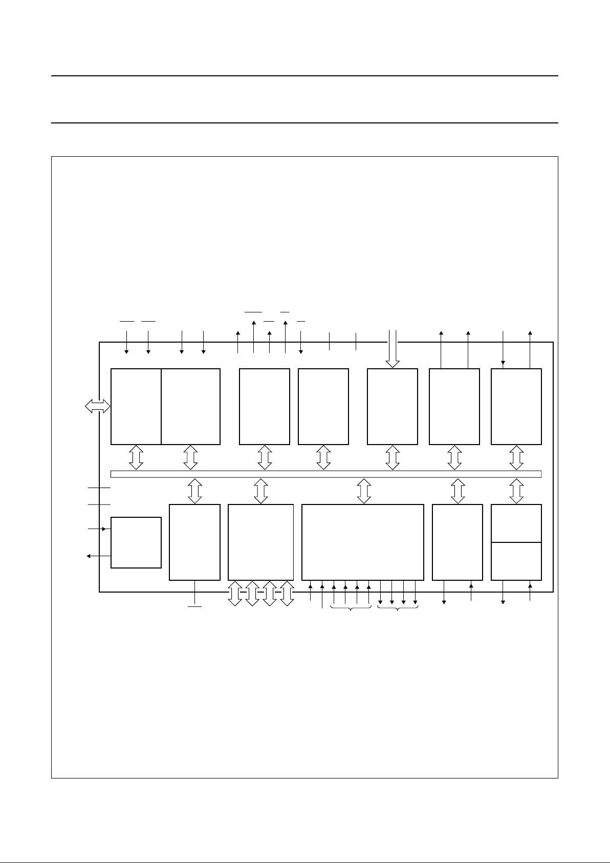
4 BLOCK DIAGRAM
Fig.1 Block diagram P8xC591.
handbook, full pagewidth
MHI001
16-BIT TIMER/EVENT
COUNTER WITH CAPTURE
(T2)
PARALLEL
I/O PORTS
WATCHDOG
TIMER (T3)
TWO 16-BIT
TIMER/EVENT
COUNTERS
(T0/T1)
16 KBYTES
PROGRAM
MEMORY
512 BYTES
DATA
MEMORY
CPU
CORE
OSCILLATOR
I
2
C SERIAL
INTERFACE
CPU
INTERFACE
(SFRs)
TXDCSCLSDA
RT2
T2
P3P2P1P0RST
A0 to A7
V
DD
V
SS
XTAL2
XTAL1
CMSR0 to 5
CMT0 to 1
CT0x/INTx
RXDC
UART
RXD TXD
CAN 2.0 B
INTERFACE
PWM
PWM0AN0 to 5AV
ref+AVSS
EA PWM1
ADC
P8xC591
T1T0
80C51 CONFIGURABLE CORE
INT1INT0
RD
WR
PSEN
ALE
Page 6

1999 Aug 19 6
Philips Semiconductors Objective Specification
Single-chip 8-bit microcontroller with CAN controller P8xC591
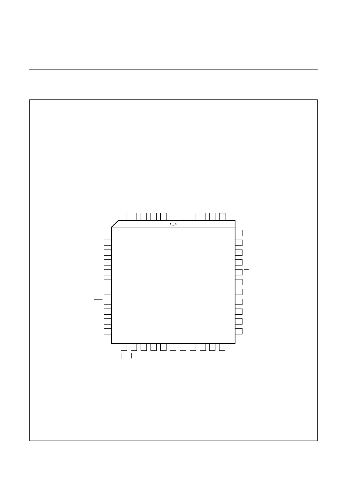
5 FUNCTIONAL DIAGRAM
Fig.2 Functional diagram.
handbook, full pagewidth
MHI002
P8xC591
(44-PIN)
0
1
2
3
4
5
6
7
PORT 0
V
DD
V
SS
0
1
2
3
4
5
6
7
PORT 1
0
1
2
3
4
5
6
7
PORT 2 address bus
AD0
AD1
AD2
AD3
AD4
AD5
AD6
AD7
and data bus
low order address
alternative functions
RXDC
CAN
I2C
TXDC
ADC0
ADC1
ADC2
ADC3
CT0I/INT2
CT1I/INT3
CT2I/INT4
CT3I/INT5
ADC4
ADC5
SCL
SDA
0
1
2
3
4
5
6
7
PORT 3
RXD
TXD
INT0
INT1
T0
T1
T2
RT2
CSMR0
CSMR1
CSMR2
CSMR3
WR
RD
AV
ref+
AV
SS
PWM1
PWM0
EA
ALE
XTAL1
XTAL2
PSEN
RST
Page 7
1999 Aug 19 7
Philips Semiconductors Objective Specification
Single-chip 8-bit microcontroller with CAN controller P8xC591
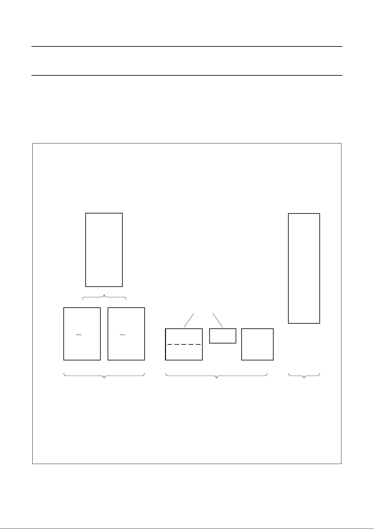
6 PINNING INFORMATION
6.1 Pinning diagram
Fig.3 Pinning Diagram for 44-lead LCC Package.
handbook, full pagewidth
P8xC591
MHI003
7
8
9
10
11
12
13
14
15
16
17
39
38
37
36
35
34
33
32
31
30
29
18
19
20
21
22
23
24
25
26
27
28
6
5
4
3
2
1
44
43
42
41
40
P1.4/ADC2/INT4/CT2I
P1.3/ADC1/INT3/CT1I
P1.2/ADC0/INT2/CT0I
P1.1/TXDC
P1.0/RXDC
AVSSAV
ref+
P0.0/AD0
P0.1/AD1
P0.2/AD2
P0.3/AD3
P3.6/WR
P3.7/RD
XTAL2
XTAL1
V
SS
V
DD
P2.0/A8
P2.1/A9
P2.2/A10
P2.3/A11
P2.4/A12
CT3I/INT5/ADC3/P1.5
SCL/ADC4/P1.6
SDA/ADC5/P1.7
RST
T2/P3.0/RXD
PWM0
RT2/P3.1/TXD
CMSR0/P3.2/INT0
CMSR1/P3.3/INT1
CMSR2/P3.4/T0
CMSR3/P3.5/T1
P0.4/AD4
P0.5/AD5
P0.6/AD6
P0.7/AD7
EA/V
PP
PWM1
ALE/PROG
PSEN
P2.7/A15
P2.6/A14
P2.5/A13
Page 8

1999 Aug 19 8
Philips Semiconductors Objective Specification
Single-chip 8-bit microcontroller with CAN controller P8xC591
Fig.4 Pinning Diagram for 44-lead Plastic Quad Flat Package (QFP).
handbook, full pagewidth
P8xC591
MHI004
1
2
3
4
5
6
7
8
9
10
11
33
32
31
30
29
28
27
26
25
24
23
12
13
14
15
16
17
18
19
20
21
22
44
43
42
41
40
39
38
37
36
35
34
P1.4/ADC2/INT4/CT2I
P1.3/ADC1/INT3/CT1I
P1.2/ADC0/INT2/CT0I
P1.1/TXDC
P1.0/RXDC
AVSSAV
ref+
P0.0/AD0
P0.1/AD1
P0.2/AD2
P0.3/AD3
P3.6/WR
P3.7/RD
XTAL2
XTAL1
V
SS
V
DD
P2.0/A8
P2.1/A9
P2.2/A10
P2.3/A11
P2.4/A12
P1.5/ADC3/INT5/CT3I
P1.6/ADC4/SCL
P1.7/ADC5/SDA
RST
P3.0/T2/RXD
PWM0
RT2/P3.1/TXD
CMSR0/P3.2/INT0
CMSR2/P3.4/T0
CMSR3/P3.5/T1
P0.4/AD4
P0.5/AD5
P0.6/AD6
P0.7/AD7
EA/V
PP
PWM1
ALE/PROG
PSEN
P2.7/A15
P2.6/A14
P2.5/A13
CMSR1/P3.3/INT1
Page 9

1999 Aug 19 9
Philips Semiconductors Objective Specification
Single-chip 8-bit microcontroller with CAN controller P8xC591
6.2 Pin description
Table 1 Pin description for QFP44/PLCC44, see Note 1.
SYMBOL
PIN
DESCRIPTION
QFP44 PLCC44
RST 4 10 Reset: A Input to reset the P8xC591. It also provides a reset pulse as output
when Timer T3 overflows.
P3.0to P3.7 Port 3 (P3.0 to P3.7): 8-bit programmable I/O port lines; Port 3 can
sink/source 4 LSTTL inputs.
Port 3 pins serve alternate functions as follows:
P3.0/RXD 5 11 RXD: Serial input port for UART;
T2: T2 event input
P3.1/TXD 7 13 TXD: Serial output port for UART;
RT2: T2 timer reset signal. Rising edge triggered.
P3.2/INT0/CMSR0 8 14 INT0: External interrupt input 0;
CMSR0: Compare and Set/Reset output for Timer T2.
P3.3/INT1/
CMSR1
915INT1: External interrupt input 1;
CMSR1: Compare and Set/Reset output for Timer T2.
P3.4/T0/CMSR2 10 16 T0: Timer 0 external interrupt input;
CMSR2: Compare and Set/Reset output for Timer T2.
P3.5/T1/CMSR3 11 17 T1: Timer 1 external interrupt input;
CMSR3: Compare and Set/Reset output for Timer T2.
P3.6/WR 12 18 WR: External Data Memory Write strobe;
P3.7/RD 13 19 RD: External Data Memory Read strobe.
During reset, Port 3 will be asynchronously driven resistive HIGH.
Port 3 has four modes selected on a per bit basis by writing to the P3M1 and
P3M2 registers as follows:
P3M1.x
0
0
1
1
P3M2.x
0
1
0
1
Mode Description
Pseudo-bidirectional (standard c51 configuration default)
Push-Pull
High impedance
Open drain
XTAL2 14 20 Crystal pin 2: output of the inverting amplifier that forms the oscillator. Left
open-circuit when an external oscillator clock is used.
XTAL1 15 21 Crystal pin 1: input to the inverting amplifier that forms the oscillator, and
input to the internal clock generator. Receives the external oscillator clock
signal when an external oscillator is used.
V
SS
16 22 Ground; circuit ground potential.
V
DD
17 23 Power supply; power supply pin during normal operation and power
reduction modes.
Page 10

1999 Aug 19 10
Philips Semiconductors Objective Specification
Single-chip 8-bit microcontroller with CAN controller P8xC591
P2.0/A08 to
P2.7/A15
18 to 25 24 to 31 Port 2 (P2.0 to P2.7): 8-bit programmable I/O port lines;
A08 to A15: High-order address byte for external memory.
Alternate function: High-order address byte for external memory (A08-A15).
Port 2 is also used to input the upper order address during EPROM
programming and verification. A8 is on P2.0, A9 on P2.1, through A12 on
P2.4.
During reset, Port 2 will be asynchronously driven HIGH.
Port 2 has four output modes selected on a per bit basis by writing to the
P2M1 and P2M2 registers as follows:
P2M1.x
0
0
1
1
P2M2.x
0
1
0
1
Mode Description
Pseudo-bidirectional (standard c51 configuration default)
Push-Pull
High impedance
Open drain
PSEN 26 32 Program Store Enable output: read strobe to the external Program Memory
via Ports 0 and 2. Is activated twice each machine cycle during fetches from
external Program Memory. When executing out of external Program Memory
two activations of PSEN are skipped during each access to external Data
Memory. PSEN is not activated (remains HIGH) during no fetches from
external Program Memory. PSEN can sink/source 8 LSTTL inputs. It can
drive CMOS inputs without external pull-ups.
ALE/PROG 27 33 Address Latch Enable output. Latches the low byte of the address during
access of external memory in normal operation. It is activated every six
oscillator periods except during an external Data Memory access. ALE can
sink/source 8 LSTTL inputs. It can drive CMOS inputs without an external
pull-up. To prohibit the toggling of ALE pin (RFI noise reduction) the bit A0
(SFR: AUXR.0) must be set by software; see Table 4.
PROG: the programming pulse input; alternative function for the P87C591.
EA/V
PP
29 35 External Access input. If, during reset, EA is held at a TTL level HIGH the
CPU executes out of the internal Program Memory. If, during reset, EA is held
at a TTL level LOW the CPU executes out of external Program Memory via
Port 0 and Port 2. EA is not allowed to float. EA is latched during reset and
don’t care after reset.
VPP: the programming supply voltage; alternative function for the P87C591.
P0.0/AD0 to
P0.7/AD7
30 to 37 36 to 43 Port 0: 8-bit open-drain bidirectional I/O port.
During reset, Port 0 is HIGH-Impedance (Tri-State).
AD7 to AD0: Multiplexed Low-order address and Data bus for external
memory. During these accesses internal pull-ups are activated. Port 0 can
sink/source up to 8 LSTTL inputs.
AV
ref+
38 44 Analog to Digital Conversion Reference Resistor: High-end.
AV
SS
39 1 Analog ground.
SYMBOL
PIN
DESCRIPTION
QFP44 PLCC44
Page 11

1999 Aug 19 11
Philips Semiconductors Objective Specification
Single-chip 8-bit microcontroller with CAN controller P8xC591
Notes
1. To avoid “latch-up” effect as power-on, the voltage on any pin at any time must not be higher or lower than VDD+0.5 V
or VSS−0.5 V.
2. Not implemented for P1.6 and P1.7.
P1.0 to P1.4
P1.5 to P1.7
40 to 44
1to3
2to6
7to9
Port 1: 8-bit I/O port with a user configurable output type. The operation of
Port 1 pins as inputs or outputs depends upon the port configuration selected.
Each port pin is configured independently.
Port 1 also provides various special functions as described below:
P1.0 40 2 RXDC: CAN Receiver input line.
P1.1 41 3 TXDC: CAN Transmit output line.
During reset, Port P1.0 and P1.1 will be asynchronously driven resistive
HIGH, P1.2 to P1.7 is High-Impedance (Tri-state).
P1.2 to P1.4 42 to 44 4 to 6 CT0I/INT2 / CT1I/INT3 / CT2I/INT4: T2 Capture timer inputs or External
Interrupt inputs.
P1.5 to P1.7 1 to 3 7 to 9
ADC0 to ADC2: Alternate function: Input channels to ADC.
ADC3 to ADC5: Input channels to ADC:
P1.5 1 7 CT3I/INT5: T2 Capture timer input or External Interrupt inputs.
P1.6 2 8 SCL: Serial port clock line I2C.
P1.7 3 9 SDA: Serial data clock line I2C.
Port 1 has four modes selected on a per bit basis by writing to the P1M1 and
P1M2 registers as follows:
P1M1.x
0
0
1
1
P1M2.x
0
1
0
1
Mode Description
Pseudo-bidirectional (standard c51 configuration default
(2)
)
Push-Pull
(2)
High impedance
Open drain
Port 1 is also used to input the lower order address byte during EPROM
programming and verification. A0 is on P1.0, etc.
PWM0 6 12 Pulse Width Modulation: Output 0.
PWM1 28 34 Pulse Width Modulation: Output 1.
SYMBOL
PIN
DESCRIPTION
QFP44 PLCC44
Page 12
1999 Aug 19 12
Philips Semiconductors Objective Specification
Single-chip 8-bit microcontroller with CAN controller P8xC591
7 MEMORY ORGANIZATION
The Central Processing Unit (CPU) manipulates operands in three memory spaces as follows (see Fig.5):
• 16 kbytes internal resp. 64 kbytes external Program Memory
• 512 bytes internal Data Memory Main-and Auxiliary RAM
• up to 64 kbytes external Data Memory (with 256 bytes residing in the internal Auxiliary RAM).
Fig.5 Memory map and address space with EXTRAM = 0.
handbook, full pagewidth
MHI005
INDIRECT ONLY
DIRECT AND
INDIRECT
AUXILIARY
RAM
(EXTRAM = 0)
SFRs
255
127
0
EXTERNAL
(EA = 0)
INTERNAL
(EA = 1)
MAIN RAM
INTERNAL DATA MEMORY
EXTERNAL
DATA MEMORY
PROGRAM MEMORY
EXTERNAL
64K
64K
16384
16383
0
OVERLAPPED SPACE
256
Page 13

1999 Aug 19 13
Philips Semiconductors Objective Specification
Single-chip 8-bit microcontroller with CAN controller P8xC591
7.1 Program Memory
The P8xC591 contains 16 Kbytes of on-chip Program
Memory which can be extended to 64 Kbytes with external
memories. When EA pin is held HIGH, the P8xC591
fetches instructions from internal ROM unless the address
exceeds 3FFFh. Locations 4000h to FFFFh are fetched
from external Program Memory. When the EA pin is held
LOW, all instruction fetches are from external memory.
The EA pin is latched during reset and is “don’t care” after
reset.
Both, for the ROM and EPROM version of the P8xC591,
precautions are implemented to protect the device against
illegal Program Memory code reading.
7.2 Addressing
The P8xC591 has five methods for addressing the
Program and Data memory:
• Register
• Direct
• Register-Indirect
• Immediate
• Base-Register plus Index-Register-Indirect.
For more details about Addressing modes please refer to
Section 22.1 “Addressing Modes”.
7.3 Expanded Data RAM addressing
The P8xC591 has internal data memory that is mapped
into four separate segments: the lower 128 bytes of RAM,
upper 128 bytes of RAM, 128 bytes Special Function
Register (SFR), and 256 bytes Auxiliary RAM (AUX-RAM)
as shown in Figure 5.
The four segments are:
1. The Lower 128 bytes of RAM (addresses 00H to 7FH)
are directly and indirectly addressable (see Fig.6).
2. The Upper 128 bytes of RAM (addresses 80H to FFH)
are indirectly addressable.
3. The Special Function Registers, SFRs, (addresses
80H to FFH) are directly addressable only. All these
SFRs are described in Table 4.
4. The 256-bytes AUX-RAM (00H - FFH) are indirectly
accessed by move external instruction, MOVX, and
within the EXTRAM bit cleared, see Table 3.
The Lower 128 bytes can be accessed by either direct or
indirect addressing. The Upper 128 bytes can be
accessed by indirect addressing only. The Upper 128
bytes occupy the same address space as the SFR. That
means they have the same address, but are physically
separate from SFR space.
When an instruction accesses an internal location above
address 7FH, the CPU knows whether the access is to the
upper 128 bytes of data RAM or to SFR space by the
addressing mode used in the instruction. Instructions that
use direct addressing access SFR space.
For example:
MOV 0A0H,#data
accesses the SFR at location 0A0H (which is P2).
Instructions that use indirect addressing access the Upper
128 bytes of data RAM.
For example:
MOV @ R0,#data
where R0 contains 0A0H, accesses the data byte at
address 0A0H, rather than P2 (whose address is 0A0H).
The AUX-RAM can be accessed by indirect addressing,
with EXTRAM bit cleared and MOVX instructions. This
part of memory is physically located on-chip, logically
occupies the first 256-bytes of external data memory.
With EXTRAM = 0, the AUX-RAM is indirectly addressed,
using the MOVX instruction in combination with any of the
registers R0, R1 of the selected bank or DPTR. An access
to AUX-RAM will not affect ports P0, P3.6 (WR#) and P3.7
(RD#). P2 SFR is output during external addressing. For
example, with EXTRAM = 0,
MOV @ R0,#data
where R0 contains 0A0h, access the AUX-RAM at
address 0A0H rather than external memory. An access to
external data memory locations higher than FFH (i.e.,
0100H to FFFFH) will be performed with the MOVX DPTR
instructions in the same way as in the standard 80C51, so
with P0 and P2 as data/address bus, and P3.6 and P3.7
as write and read timing signals. Refer to Table 4.
With EXTRAM = 1, MOVX @ Ri and MOVX @ DPTR will
be similar to the standard 80C51. MOVX @ Ri will provide
an 8-bit address multiplexed with data on Port 0 and any
output port pins can be used to output higher order
address bits. This is to provide the external paging
capability. MOVX @ DPTR will generate a 16-bit address.
Port 2 outputs the high-order eight address bits (the
contents of DPH) while Port 0 multiplexes the low-order
eight address bits (DPL) with data. MOVX @ Ri and MOVX
@ DPTR will generate either read or write signals on P3.6
(#WR) and P3.7 (#RD).
The stack pointer (SP) may be located anywhere in the
256 bytes RAM (lower and upper RAM) internal data
memory. The stack cannot be located in the AUX-RAM.
Page 14

1999 Aug 19 14
Philips Semiconductors Objective Specification
Single-chip 8-bit microcontroller with CAN controller P8xC591
Table 2 AUX-RAM Page Register (address 8EH)
Table 3 Description of AUX-RAM bits
Notes
1. User software should not write ‘1’s to reserved bits. These bits may be used in future 80C51 family products to invoke
new features. In that case, the reset or inactive of the new bit will be 0, and its active value will be ‘1’. The value read
from a reserved bit is indeterminate.
2. Reset value is ‘xxxxxx10B’.
76543210
- - - - - LVADC EXTRAM AO
BIT SYMBOL FUNCTION
7 to 3 − Reserved for future use; see Note 1.
2 LVADC Enable A/D low voltage operation.
LVADC
0
1
Operating Mode
Turns off A/D charge pump.
Turns on A/D charge pump. Required for operation below 4 V.
1 EXTRAM Internal/External RAM (00H - FFH) access using MOVX @ RI / @ DPTR
EXTRAM
0
1
Operating Mode
Internal AUX-RAM (00H - FH) access using MOVX @ RI / @ DPTR.
External data memory access.
0 AO Disable/Enable ALE.
AO
0
1
Operating Mode
ALE is permitted at a constant rate of 1/6 the oscillator frequency.
ALE is active only during a MOVX or MOVC instruction.
Page 15

1999 Aug 19 15
Philips Semiconductors Objective Specification
Single-chip 8-bit microcontroller with CAN controller P8xC591
Fig.6 Internal Main RAM bit addresses.
handbook, full pagewidth
MHI006
7F 7E 7D 7C 7B 7A 79 78
77 76 75 74 73 72 71 70
6F 6E 6D 6C 6B 6A 69 68
67 66 65 64 63 62 61 60
5F 5E 5D 5C 5B 5A 59 58
57 56 55 54 53 52 51 50
4F 4E 4D 4C 4B 4A 49 48
47 46 45 44 43 42 41 40
3F 3E 3D 3C 3B 3A 39 38
37 36 35 34 33 32 31 30
2F 2E 2D 2C 2B 2A 29 28
27 26 25 24 23 22 21 20
1F 1E 1D 1C 1B 1A 19 18
17 16 15 14 13 12 11 10
0F 0E 0D 0C 0B 0A 09 08
07 06 05 04 03 02 01 00
18h
17h
10h
0Fh
08h
07h
00h
24
23
31
16
15
8
7
0
REGISTER BANK 3
REGISTER BANK 2
REGISTER BANK 1
REGISTER BANK 0
32
33
34
35
36
37
38
39
40
41
42
43
44
45
46
47
(MSB) (LSB)
127
7Fh
2Fh
2Eh
2Dh
2Ch
2Bh
2Ah
29h
28h
27h
26h
25h
24h
23h
22h
21h
20h
1Fh
Page 16
1999 Aug 19 16
Philips Semiconductors Objective Specification
Single-chip 8-bit microcontroller with CAN controller P8xC591
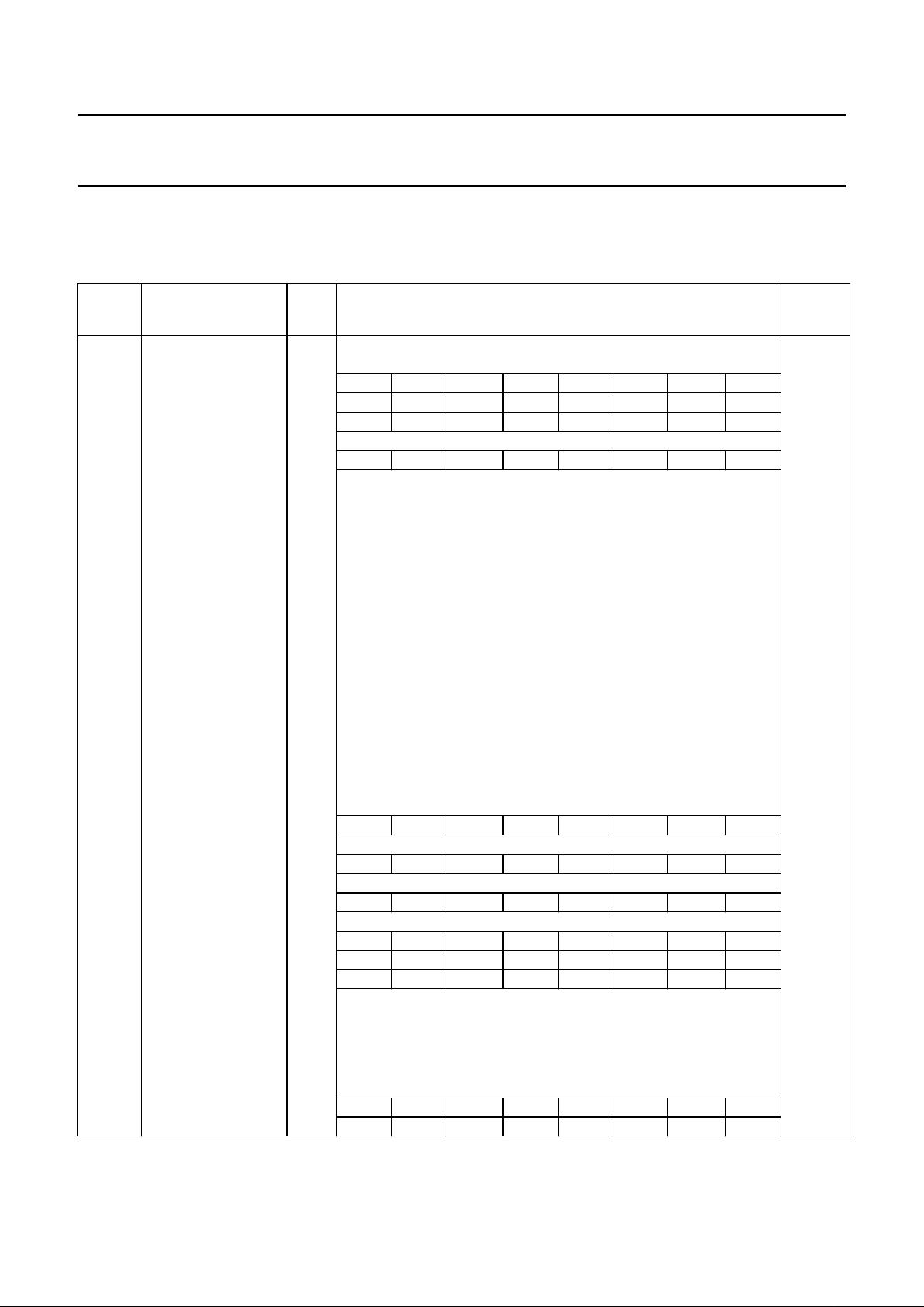
7.3.1 SPECIAL FUNCTION REGISTERS
Table 4 Special Function Register Bit Address, Symbol or Alternate Port Function
* = SFRs are bit addressable; # = SFRs are modified from or added to the 80C51 SFRs.
NAME DESCRIPTION
SFR
ADDR
BIT FUNCTIONS AND ADDRESSES
RESET
VALUE
MSB LSB
ACC* Accumulator E0H E7 E6 E5 E4 E3 E2 E1 E0 00H
ADCH# A/D converter high C6H xxxxxxxxb
ADCON# A/D control C5H ADC.1 ADC.0 - ADCI ADCS AADR2 AADR1 AADR0 xx000000b
AUXR Auxiliary 8EH - - - - - LVADC EXTRAM A0 xxxxx110B
AUXR1 Auxiliary A2H ADC8 AIDL SRST WDE WUPD 0 - DPS 000000x0B
B* B register F0H F7 F6 F5 F4 F3 F2 F1 F0 00H
CTCON# Capture control EBH CTN3 CTP3 CTN2 CTP2 CTN1 CTP1 CTN0 CTP0 00H
CTH3# Capture high 3 CFH xxxxxxxxB
CTH2# Capture high 2 CEH xxxxxxxxB
CTH1# Capture high 1 CDH xxxxxxxxB
CTH0# Capture high 0 CCH xxxxxxxxB
CMH2# Compare high 2 CBH 00H
CMH1# Compare high 1 CAH 00H
CMH0# Compare high 0 C9H 00H
CTL3# Capture low 3 AFH xxxxxxxxB
CTL2# Capture low 2 AEH xxxxxxxxB
CTL1# Capture low 1 ADh xxxxxxxxB
CTL0# Capture low 0 ACH xxxxxxxxB
CML2# Compare low 2 ABH 00H
CML1# Compare low 1 AAH 00H
CML0# Compare low 0 A9H 00H
DPTR: Data Pointer (2 bytes):
DPH Data Pointer High 83h 00H
DPL Data Pointer Low 82h 00H
AF AE AD AC AB AA A9 A8
IENO*# Interrupt Enable 0 A8H EA EAD ES1 ES0 ET1 EX1 ET0 EX0 00H
EF EE ED EC EB EA E9 E8
IEN1*# Interrupt Enable 1 E8H ET2 ECAN ECM1 ECM0 ECT3 ECT2 ECT1 ECT0 00H
BF BE BD BC BB BA B9 B8
IP0*# Interrupt Priority 0 B8H - PAD PS1 PS0 PT1 PX1 PT0 PX0 x0000000B
FF FE FD FC FB FA F9 F8
IP0H Interrupt Priority 0 high B7H - PADH PS1H PS0H PT1H PX1H PT0H PX0H x0000000B
IP1*# Interrupt Priority 1 F8h PT2 PCAN PCM1 PCM0 PCT3 PCT2 PCT1 PCT0 00H
IP1H Interrupt Priority 1 high F7H PT2H PCANH PCM1H PCM0H PCT3H PCT2H PCT1H PCT0H 00H
CANMOD CAN Mode Register C4H 00H
CANCON CAN Command (w) and
Interrupt (r)
C3H 00H
CANDAT CAN Data C2H 00H
CANADR CAN Address C1H 00H
C7 C6 C5 C4 C3 C2 C1 C0
CANSTA CAN Status (r) C0H BS ES TS RS TCS TBS DOS RBS 00H
CAN Interrupt Enable (w) BEIE ALIE EPIE WUIE DOIE EIE TIE RIE
Page 17

1999 Aug 19 17
Philips Semiconductors Objective Specification
Single-chip 8-bit microcontroller with CAN controller P8xC591
P1M1 Port 1 output mode 1 92H FCH
P1M2 Port 1 output mode 2 93H 00H
P2M1 Port 2 output mode 1 94H 00H
P2M2 Port 2 output mode 2 95H 00H
P3M1 Port 3 output mode 1 9AH 00H
P3M2 Port 3 output mode 2 9BH 00H
B7 B6 B5 B4 B3 B2 B1 B0
- - CSMR3 CSMR2 CSMR1 CSMR0 RT2 T2
P3* Port 3 B0H RD WR T1 T0 INT1 INT0 TXD RXD FFH
A7 A6 A5 A4 A3 A2 A1 A0
P2* Port 2 A0H A15 A14 A13 A12 A11 A10 A9 A8 FFH
97 96 95 94 93 92 91 90
ADC5 ADC4 ADC3 ADC2 ADC1 ADC0 −−
P1* Port 1 90H SDA SCL CT3I CT2I CT1I CT0I TXDC RXDC FFH
87 86 85 84 83 82 81 80
P0* Port 0 80H AD7 AD6 AD5 AD4 AD3 AD2 AD1 AD0 FFH
PCON Power Control 87H SMOD1 SMOD0 POF WLE GF1 GF0 PD IDL 00x00000B
PSW Program Status Word D0H CY AC F0 RS1 RS0 OV F1 P 00H
PWMP# PWM Prescaler FEH 00H
PWMP1# PWM Register 1 FDH 00H
PWMP0# PWM Register 0 FCH 00H
RTE# Reset Enable EFH RP35 RP34 RP33 RP32 xxxx0000B
S0ADDR Serial 0 Slave Address CBh 00H
S0ADEN Slave Address Mask F9H 00H
SP Stack Pointer 81H 07H
S0BUF Serial 0 Data Buffer 99H xxxxxxxxB
S0PSL Prescaler Value UART FAH 00H
S0PSH Prescaler/Value UART FBH SPS Prescaler higher nibble 0xxx0000B
9F 9E 9D 9C 9B 9A 99 98
S0CON* Serial 0 Control 98H SM0/FE SM1 SM2 REN TB8 RB8 TI RI 00H
S1CON#* Serial 1Control D8H CR2 ENS1 STA ST0 SI AA CR1 CR0 00H
S1ADR# Serial 1 Address DBH SLAVE ADDRESS GC 00H
S1DAT# Serial 1 Data DAH 00H
S1STA# Serial 1 Status D9H SC4 SC3 SC2 SC1 SC0 0 0 0 F8H
DF DE DD DC DB DA D9 D8
STE# Set Enable EEH SP35 SP34 SP33 SP32 xxxx0000B
TH1 Timer High 1 8DH 00H
TH0 Timer High 0 8CH 00H
TL1 Timer Low 1 8BH 00H
TL0 Timer Low 0 8AH 00H
TMH2# Timer High 2 EDH 00H
TML2# Timer Low 2 ECH 00H
NAME DESCRIPTION
SFR
ADDR
BIT FUNCTIONS AND ADDRESSES
RESET
VALUE
MSB LSB
Page 18

1999 Aug 19 18
Philips Semiconductors Objective Specification
Single-chip 8-bit microcontroller with CAN controller P8xC591
TMOD Timer Mode 89H GATE C/T M1 M0 GATE C/T M1 M0 00H
8F 8E 8D 8C 8B 8A 89 88
TCON* Timer Control 88H TF1 TR1 TF0 TR0 IE1 IT1 IE0 IT0 00H
TM2CON# Timer 2 Control EAH T2IS1 T2IS0 T2ER T2B0 T2P1 T2P0 T2MS1 T2MS0 00H
CF CE CD CC CB CA C9 C8
TM2IR#* Timer 2/CAN Int Flag Reg C8H T2OV CMI2/
CAN
CMI1 CMI0 CTI3 CTI2 CTI1 CTI0 00H
T3# Timer 3 FFH 00H
NAME DESCRIPTION
SFR
ADDR
BIT FUNCTIONS AND ADDRESSES
RESET
VALUE
MSB LSB
Page 19

1999 Aug 19 19
Philips Semiconductors Objective Specification
Single-chip 8-bit microcontroller with CAN controller P8xC591
Fig.7 Dual DPTR:
handbook, full pagewidth
DPH
(83H)
BT0
AUXR1
DPS
DPL
(82H)
EXTERNAL
DATA
MEMORY
DPTR0
MHI007
DPTR1
7.4 Dual DPTR
The dual DPTR structure (see Figure 7) is a way by which
the chip will specify the address of an external data
memory location. There are two 16-bit DPTR registers that
address the external memory, and a single bit called DPS
= AUXR1/bit0 that allows the program code to switch
between them.
The DPS bit status should be saved by software when
switching between DPTR0 and DPTR1.
Note that bit 2 is not writable and is always read as a zero.
This allows the DPS bit to be quickly toggled simply by
executing an INC AUXR1 instruction without affecting the
other bits.
DPTR Instructions
The instructions that refer to DPTR refer to the data pointer
that is currently selected using the AUXR1/bit 0 register.
The six instructions that use the DPTR are as follows:
INC DPTRIncrements the data pointer by 1
MCV DPTR, #data 16 Loads the DPTR with a 16-bit
constant
MOV A, @ A+DPTR Move code byte relative to
DPTR to ACC
MOVX A, @ DPTR Move external RAM (16-bit
address) to ACC
MOVX @ DPTR, A Move ACC to external RAM
(16-bit address)
JMP @ A + DPTR Jump indirect relative to
DPTR
The data pointer can be accessed on a byte-by-byte basis
by specifying the low or high byte in an instruction which
accesses the SFRs. See application note AN458 for more
details.
Page 20

1999 Aug 19 20
Philips Semiconductors Objective Specification
Single-chip 8-bit microcontroller with CAN controller P8xC591
7.4.1 AUXR1 PAGE REGISTER
Table 5 AUXR1 Page Register (address A2H)
Table 6 Description of AUXR1 of bits
User software should not write 1s to reserved bits. Theses bits may be used in future 8051 family products to invoke
new features. In that case, the reset or inactive value of the new bit will be logic 0, and its active value will be logic 1.
The value read from a reserved bit is indeterminate. The reset value of AUXR1 is (000000xB).
76543210
ADC8 AIDL SRST WDE WUPD 0 − DSP
BIT SYMBOL DESCRIPTION
7 ADC8 ADC Mode Switch. Switches between 10-bit conversion and 8-bit conversion
ADC8
0
1
Operating Mode
10-bit conversion (50 machine cycles)
8-bit conversion (24 machine cycles)
6 AIDL Enables the ADC during Idle mode.
5 SRST Software Reset.
4 WDE Watchdog Timer Enable Flag.
3 WUPD Enable Wake-up from Power-down.
20Reserved.
1 − Reserved.
0 DSP Data Pointer Switch. Switches between DPRT0 and DPTR1.
ADC8
0
1
Operating Mode
DPTR0
DPTR1
Page 21
1999 Aug 19 21
Philips Semiconductors Objective Specification
Single-chip 8-bit microcontroller with CAN controller P8xC591
8 I/O FACILITIES
The P8xC591 consists of 32 I/O Port lines with partly
multiple functions. The I/O’s are held HIGH during reset
(asynchronous, before oscillator is running).
Ports 0, 1, 2 and 3 perform the following alternative
functions:
Port 0 is the same as in the 80C51. After reset the Port
Special Function Register is set to ’FFh’ as known
from other 80C51 derivatives. Port 0 also provides
the multiplexed low-order address and data bus
used for expanding the P8xC591 with standard
memories and peripherals.
Port 1 supports several alternative functionalities. For this
reason it has different I/O stages. Note, port P1.0
and P1.1 are Driven-High and P1.2 to P1.7 are
High-Impedance (Tri-state) after reset.
Port 2 is the same as in the 80C51. After reset the Port
Special Function Register is set to ’FFh’ as known
from other 80C51 derivatives. Port 2 also provides
the high-order address bus when the P8xC591 is
expanded with external Program Memory and/or
external Data Memory.
Port 3 is the same as in the 80C51. During reset the Port
3 Special Function Register is set to ’FFh’ as known
from other 80C51 derivatives.
9 OSCILLATOR CHARACTERISTICS
XTAL1 and XTAL2 are the input and output, respectively,
of an inverting amplifier. The pins can be configured for
use as an on-chip oscillator, as shown in the logic symbol.
To drive the device from an external clock source, XTAL1
should be driven while XTAL2 is left unconnected. There
are no requirements on the duty cycle of the external clock
signal. However, minimum and maximum high and low
times specified in the data sheet must be observed.
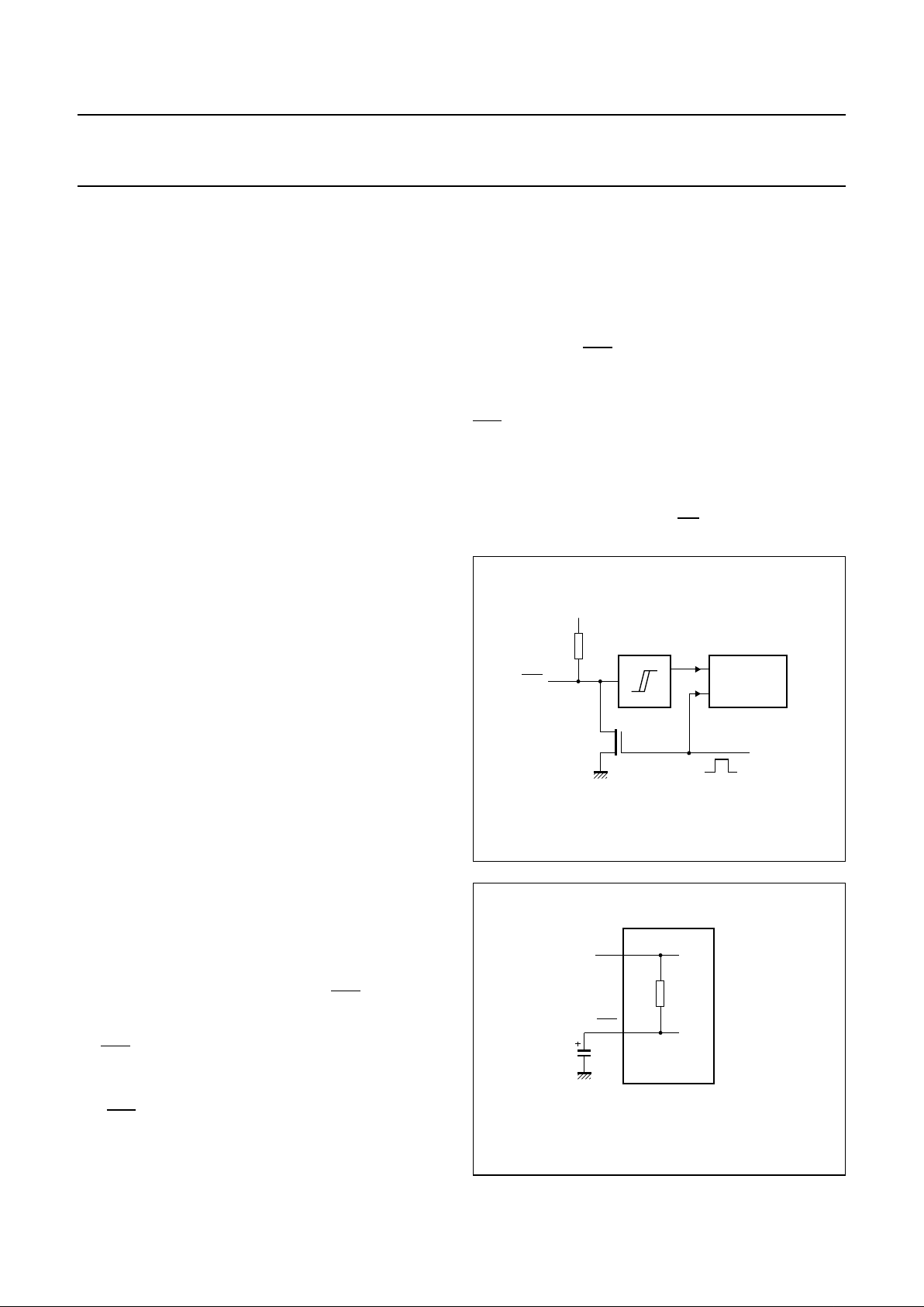
10 RESET
A reset is accomplished by holding the RST pin LOW for
at least two machine cycles (12 oscillator periods), while
the oscillator is running. To insure a good power-on reset,
theRST pin must be low long enough to allow the oscillator
time to start up (normally a few milliseconds) plus two
machine cycles.
The RST line can also be pulled LOW internally by a
pull-down transistor activated by the watchdog timer T3.
The length of the output pulse from T3 is 3 machine cycles.
A pulse of such short duration is necessary in order to
recover from a processor or system fault as fast as
possible.
Note that the short reset pulse from Timer T3 cannot
discharge the power-on reset capacitor (see Figure 8).
Consequently, when the watchdog timer is also used to set
external devices, this capacitor arrangement should not be
connected to the RST pin, and a different circuit should be
used to perform the power-on reset operation. A timer T3
overflow, if enabled, will force a reset condition to the
P8xC591 by an internal connection, whether the output
RST is pulled-up HIGH or not.
A reset may be performed in software by setting the
software reset bit, SRST (AUXR1.5).
This device also has a Power-on Detect Reset circuit as
VCC transitions from VCC past V
RST
.
Fig.8 On-Chip Reset Configuration.
handbook, halfpage
MHI008
SCHMITT
TRIGGER
RESET
CIRCUITRY
RST
overflow
timer T3
on-chip
resistor
V
DD
Fig.9 Power-on Reset.
handbook, halfpage
MHI009
RST
R
RST
2.2 µF
P8xC591
V
DD
Page 22

1999 Aug 19 22
Philips Semiconductors Objective Specification
Single-chip 8-bit microcontroller with CAN controller P8xC591
11 LOW POWER MODES
11.1 Stop Clock Mode
The static design enables the clock speed to be reduced
down to 0 MHz (stopped). When the oscillator is stopped,
the RAM and Special Function Registers retain their
values. This mode allows step-by-step utilization and
permits reduced system power consumption by lowering
the clock frequency down to any value. For lowest power
consumption the Power-down mode is suggested.
11.2 Idle Mode
In the Idle mode (see Table 7), the CPU puts itself to sleep
while all of the on-chip peripherals stay active. The
instruction to invoke the idle mode is the last instruction
executed in the normal operating mode before the Idle
mode is activated. The CPU contents, the on-chip RAM,
and all of the special function registers remain intact during
this mode. The Idle mode can be terminated either by any
enabled interrupt (at which time the process is picked up
at the interrupt service routine and continued), or by a
hardware reset which starts the processor in the same
manner as a Power-on reset.
11.3 Power-down Mode
To save even more power, a Power-down mode (see
Table 7) can be invoked by software. In this mode, the
oscillator is stopped and the instruction that invoked Power
Down is the last instruction executed. The on-chip RAM
and Special Function Registers retain their values down to
2.0 V and care must be taken to return VCCto the minimum
specified operating voltages before the Power-down Mode
is terminated.
A hardware reset or external interrupt can be used to exit
from Power-down. The Wake-up from Power-down bit,
WUPD (AUXR1.3) must be set in order for an interrupt to
cause a Wake-up from Power-down. Reset redefines all
the SFRs but does not change the on-chip RAM. A
Wake-up allows both the SFRs and the on-chip RAM to
retain their values.
To properly terminate Power-down the reset or external
interrupt should not be executed before VCC is restored to
its normal operating level and must be held active long
enough for the oscillator to restart and stabilize (normally
less than 10 ms).
Table 7 Status of external pins during Idle and Power-down modes
With an external interrupt, INT0 and INT1 must be enabled and configured as level-sensitive. Holding the pin low restarts
the oscillator but bringing the pin back high completes the exit. Once the interrupt is serviced, the next instruction to be
executed after RETI will be the one following the instruction that put the device into Power-down.
MODE MEMORY ALE PSEN PORT 0 PORT 1 PORT 2 PORT 3
PWM0/
PWM1
Idle internal 1 1 port data port data port data port data high
external 1 1 float port data address port data high
Power-down internal 0 0 port data port data port data port data high
external 0 0 float port data port data port data high
Page 23

1999 Aug 19 23
Philips Semiconductors Objective Specification
Single-chip 8-bit microcontroller with CAN controller P8xC591
11.3.1 POWER OFF FLAG
The Power Off Flag (POF) is set by on-chip circuitry when
the VCC level on the P8xC591 rises from 0 to 5 V. The POF
bit can be set or cleared by software allowing a user to
determine if the reset is the result of a power-on or warm
after Power-down. The VCC level must remain above 3 V
for the POF to remain unaffected by the VCC level.
11.3.2 DESIGN CONSIDERATION
• When the Idle mode is terminated by a hardware reset,
the device normally resumes program execution, from
where it left off, up to two machine cycles before the
internal reset algorithm takes control. On-chip hardware
inhibits access to internal RAM in this event, but access
to the port pins is not inhibited. To eliminate the
possibility of an unexpected write when Idle is
terminated by reset, the instruction following the one
that invokes Idle should not be one that writes to a port
pin or to external memory.
11.3.3 ONCE
TM
MODE
The ONCETM (“On-Circuit Emulation”) Mode facilities
testing and debugging of systems without the device
having to be removed from the circuit. The ONCE Mode is
invoked by:
1. Pull ALE low while the device is in reset an PSEN is
high,
2. Hold ALE low as RST is deactivated.
While the device is in ONCE Mode, the Port 0 pins go into
a float state, and the other port pins and ALE and PSEN
are weakly pulled high. The oscillator circuit remains
active. While the device is in this mode, an emulator or test
CPU can be used to drive the circuit. Normal operation is
restored when a normal reset is applied.
11.3.4 REDUCED EMI MODE
The ALE-Off bit, AO (AUXR.0) can be set to 0 disable the
ALE output. It will automatically become active when
required for external memory accesses and resume to the
OFF state after completing the external memory access.
11.3.5 P
OWER CONTROL REGISTER (PCON)
Table 8 Power Control Register (address 87H)
Table 9 Description of PCON bits
If logic 1s are written to PD and IDL at the same time, PD takes precedence. The reset value of PCON is (0XX00000).
76543210
SMOD1 SMOD0 POF WLE GF1 GF0 PD IDL
BIT SYMBOL DESCRIPTION
7 SMOD1 Double Baud rate. When set to logic 1 the baud rate is doubled when the serial port
SIO0 is being used in Modes 1, 2 and 3.
6 SMOD0 Double Baud rate. Selects SM0/FE for SCON.7 bit.
5 POF Power Off flag.
4 WLE Watchdog Load Enable. This flag must be set by software prior to loading T3
(Watchdog Timer). It is cleared when T3 is loaded.
3 GF1 General purpose flag bits.
2 GF0
1PDPower-down mode select. Setting this bit activates Power-down mode. It can only be
set if the Watchdog timer enable bit ‘WDE’ is set to logic 0.
0 IDL Idle mode select. Setting this bit activates the Idle mode.
Page 24

1999 Aug 19 24
Philips Semiconductors Objective Specification
Single-chip 8-bit microcontroller with CAN controller P8xC591
12 CAN, CONTROLLER AREA NETWORK
Controller Area Network is the definition of a high
performance communication protocol for serial data
communication. The CAN controller circuitry is designed to
provide a full implementation of the CAN-Protocol
according to the CAN Specification Version 2.0 B.
Microcontroller including this on-chip CAN Controller are
used to build powerful local networks, both for general
industrial and automotive environments. The result is a
strongly reduced wiring harness and enhanced diagnostic
and supervisory capabilities.
The P8xC591 includes the same functions known from the
SJA1000 stand-alone CAN Controller from Philips
Semiconductors with the following improvements:
• Enhanced receive interrupt
• Enhanced acceptance filter
– 8 filter for standard frame formats
– 4 filter for extended formats
– “change on the fly” feature.
12.1 Features of the PeliCAN Controller
12.1.1 GENERAL CAN FEATURES
• CAN 2.0B protocol compatibility
• Multi-master architecture
• Bus access priority determined by the message
identifier (11 bit or 29 bit)
• Non destructive bit-wise arbitration
• Guaranteed latency time for high priority messages
• Programmable transfer rate (up to 1Mbit/s)
• Multicast and broadcast message facility
• Data length from 0 up to 8 bytes
• Powerful error handling capability
• Non-return-to-zero (NRZ) coding/decoding with
bit-stuffing
• Suitable for use in a wide range of networks including
SAE’s network classes A, B, C.
12.1.2 P8XC591 PELICAN FEATURES (ADDITIONAL TO
CAN 2.0B)
• Supports 11-bit identifier as well as 29-bit identifier
• Bit rates up to 1 Mbit/s
• Error Counters with read / write access
• Programmable Error Warning Limit
• Arbitration Lost Interrupt with detailed bit position
• Single Shot Transmission (no re-transmission)
• Listen Only Mode (no acknowledge, no active error
flags)
• Hot Plugging support (software driven bit rate detection)
• Extended receive buffer (FIFO, 64 byte)
• Receive Buffer level sensitive Receive Interrupt
• High Priority Acceptance Filters for Receive Interrupt
• Acceptance Filters with “change on the fly” feature
• Reception of “own” messages (Self Reception Request)
• Programmable CAN output driver configuration
Page 25
1999 Aug 19 25
Philips Semiconductors Objective Specification
Single-chip 8-bit microcontroller with CAN controller P8xC591
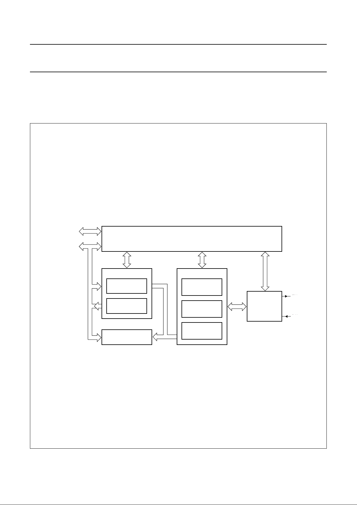
12.2 PeliCAN structure
A 80C51 CPU Interface connects the PeliCAN to the internal bus of the P8xC591 microcontroller. Via five Special
Function Registers CANADR, CANDAT, CANMOD, CANSTA and CANCON the CPU has access to the PeliCAN. The
SFR will described later on.
Fig.10 Block Diagram of the PeliCAN.
handbook, full pagewidth
MHI010
PeliCAN Core BlockMESSAGE BUFFER
ERROR
MANAGEMENT
LOGIC
TRANSMIT
BUFFER
control
address/data
RECEIVE
FIFO
ACCEPTANCE
FILTER
BIT
TIMING
LOGIC
TRANSMIT
MANAGEMENT
LOGIC
INTERFACE
MANAGEMENT
LOGIC
TX
RX
BIT
STREAM
PROCESSOR
TXDC
RXDC
Page 26

1999 Aug 19 26
Philips Semiconductors Objective Specification
Single-chip 8-bit microcontroller with CAN controller P8xC591
12.2.1 INTERFACE MANAGEMENT LOGIC (IML)
The Interface Management Logic interprets commands
from the CPU, controls addressing of the CAN Registers
and provides interrupts and status information to the CPU.
Additionally it drives the universal interface of the PeliCAN.
12.2.2 TRANSMIT BUFFER (TXB)
The Transmit Buffer is an interface between the CPU and
the Bit Stream Processor (BSP) and is able to store a
complete CAN message which should be transmitted over
the CAN network. The buffer is 13 bytes long, written by
the CPU and read out by the BSP or the CPU itself.
12.2.3 RECEIVE BUFFER (RXB, RXFIFO)
The Receive Buffer is an interface between the
Acceptance Filter and the CPU and stores the received
and accepted messages from the CAN Bus line. The
Receive Buffer (RXB) represents a CPU-accessible
13-byte-window of the Receive FIFO (RXFIFO), which has
a total length of 64 bytes depending on the
implementation. With the help of this FIFO the CPU is able
to process one message while other messages are being
received.
12.2.4 ACCEPTANCE FILTER (ACF)
The Acceptance Filter compares the received identifier
with the Acceptance Filter Table contents and decides
whether this message should be accepted or not. In case
of a positive acceptance test, the complete message is
stored in the RXFIFO. The ACF contains 4 independent
Acceptance Filter banks supporting extended and
standard CAN frames with “change on the fly” feature.
12.2.5 B
IT STREAM PROCESSOR (BSP)
The Bit Stream Processor is a sequencer, controlling the
data stream between the Transmit Buffer, RXFIFO and the
CAN-Bus. It also performs the error detection, arbitration,
stuffing and error handling on the CAN bus.
12.2.6 ERROR MANAGEMENT LOGIC (EML)
The EML is responsible for the error confinement of the
transfer-layer modules. It gets error announcements from
the BSP and then informs the BSP and IML about error
statistics.
12.2.7 B
IT TIMING LOGIC (BTL)
The Bit Timing Logic monitors the serial CAN bus line and
handles the Bus line-related bit timing. It synchronizes to
the bit stream on the CAN Bus on a “recessive” to
“dominant” Bus line transition at the beginning of a
message (hard synchronization) and resynchronizes on
further transitions during the reception of a message (soft
synchronization). The BTL also provides programmable
time segments to compensate for the propagation delay
times and phase shifts (e.g., due to oscillator drifts) and to
define the sampling time and the number of samples to be
taken within a bit time.
12.2.8 TRANSMIT MANAGEMENT LOGIC (TML)
The Transmit Management Logic provides the driver
signals for the push-pull CAN TX transistor stage.
Depending on the programmable output driver
configuration the external transistors are switched on or
off. Additionally a short circuit protection and the
asynchronous float on hardware reset is performed here.
Page 27

1999 Aug 19 27
Philips Semiconductors Objective Specification
Single-chip 8-bit microcontroller with CAN controller P8xC591
12.3 Communication between PeliCAN Controller
and CPU
A 80C51 CPU Interface connects the PeliCAN to the
internal bus of an 80C51 microcontroller. Special Function
Registers, allows a smart and fast access to the PeliCAN
registers and RAM area. Because of the big address range
to be supported, an indirect pointer based addressing is
included allowing a fast register access with address
autoincrement mode. This reduces the needed number of
Special Function Registers to an amount of 5.
• Five Special Function Registers (SFRs)
• Register address generation in auto-increment mode
• Access to the complete address range of the PeliCAN
Fig.11 CPU to CAN Interfacing.
handbook, full pagewidth
MHI020
data
80C51
CORE
write
read
SFRs
PeliCAN
address
CANDAT
CANADR
INTERFACE CAN CONTROLLER
CANSTA
CANCON
CANMOD
12.3.1 SPECIAL FUNCTION REGISTERS
Via the five Special Function Registers CANADR,
CANDAT, CANMOD, CANSTA and CANCON the CPU
has access to the PeliCAN Block. Note that CANCON and
CANSTA have different registers mapped depending on
the direction of the access.
The PeliCAN registers may be accessed in two different
ways. The most important registers, which should support
software polling or are controlling major CAN functions are
accessible directly as separate SFRs. Other parts of the
PeliCAN Block are accessible using an indirect pointer
mechanism. In order to achieve a high data throughput
even if the indirect access is used, an address
auto-increment feature is included here.
Page 28

1999 Aug 19 28
Philips Semiconductors Objective Specification
Single-chip 8-bit microcontroller with CAN controller P8xC591
Table 10 CAN Special Function Registers
SFR ACCESS
PELICAN
REG.
BIT7 BIT6 BIT5 BIT4 BIT3 BIT2 BIT1 BIT0
SFR
ADDR
CANADR Read/
Write
- CANA7 CANA6 CANA5 CANA4 CANA3 CANA2 CANA1 CANA0 C1
CANDAT Read/
Write
- CAND7 CAND6 CAND5 CAND4 CAND3 CAND2 CAND1 CAND0 C2
CANMOD Read/
Write
Mode TM RIPM RPM SM − STM LOM RM C4
CANSTA Read Status BS ES TS RS TCS TBS DOS RBS C0
Write Interrupt
Enable
BEIE ALIE EPIE WUIE DOIE EIE TIE RIE
CANCON Read Interrupt BEI ALI EPI WUI DOI EI TI RI C3
Write Command - - - SRR CDO RRB AT TR
12.3.2 CANADR
This read/write register defines the address of one of the
PeliCAN internal registers to be accessed via CANDAT. It
could be interpreted as a pointer to the PeliCAN.
The read and write access to the PeliCAN Block register is
performed using the CANDAT register.
With the implemented auto address increment mode a fast
stack-like reading and writing of CAN Controller internal
registers is provided. IF the currently defined address
within CANADR is above or equal to 32 decimal, the
content of CANADR is incremented automatically after any
read or write access to CANDAT. For instance, loading a
message into the Transmit Buffer can be done by writing
the first Transmit Buffer Address (112 decimal) into
CANADR and then moving byte by byte of the message to
CANDAT. Incrementing CANADR beyond FFh resets
CANADR to 00h.
In case CANADR is below 32 decimal, there is no
automatic address incrementation performed. CANADR
keeps its value even if CANDAT is accessed for reading or
writing. This is to allow polling of registers in the lower
address space of the PeliCAN Controller.
12.3.3 CANDAT REGISTER
CANDAT is implemented as a read/write register.
The Special Function Register CANDAT appears as a port
to the CAN Controller’s internal register (memory location)
being selected by CANADR. Reading or writing CANDAT
is effectively an access to that PeliCAN internal register,
which is selected by CANADR. CANDAT is implemented
as a read/write register.
Note that any access to this register automatically
increments CANADR if the current address within
CANADR is above ore equal to 32 decimal.
12.3.4 CANMOD
With a read or write access to CANMOD the Mode
Register of the PeliCAN is accessed directly. The Mode
register is located at address 00h within the PeliCAN
Block.
12.3.5 CANSTA
The CANSTA SFR provides a direct access to the Status
Register of the PeliCAN as well as to the Interrupt Enable
Register, depending on the direction of the access.
Reading CANSTA is an access to the Status Register of
the PeliCAN (address 2). When writing to CANSTA the
Interrupt Enable Register is accessed (address 4).
12.3.6 CANCON
The CANCON SFR provides a direct access to the
Interrupt Register of the PeliCAN as well as to the
Command register, depending on the direction of the
access.
When reading CANCON the Interrupt Register of the
PeliCAN is accessed (address 3), while writing to
CANCON means an access to the Command Register
(address 01).
Page 29

1999 Aug 19 29
Philips Semiconductors Objective Specification
Single-chip 8-bit microcontroller with CAN controller P8xC591
12.4 Register and Message Buffer description
12.4.1 ADDRESS LAYOUT
The PeliCAN internal registers appear to the host CPU as on-chip memory mapped peripheral registers. Because the
PeliCAN can operate in different modes (Operating / Reset, see also Mode Register), one have to distinguish between
different internal address definitions. Starting from CAN Address 128 the complete internal FIFO RAM is mapped to the
CPU Interface.
Table 11 Address allocation
CAN
ADDR.
OPERATING MODE RESET MODE
READ WRITE READ WRITE
0 Mode Mode Mode Mode
1 (00) Command (00) Command
2 Status - Status 3 Interrupt - Interrupt 4 Interrupt Enable Interrupt Enable Interrupt Enable Interrupt Enable
5 Rx Interrupt Level Rx Interrupt Level Rx Interrupt Level Rx Interrupt Level
6 Bus Timing 0 - Bus Timing 0 Bus Timing 0
7 Bus Timing 1 - Bus Timing 1 Bus Timing 1
8 See Note 2 - - 9 Rx Message Counter - Rx Message Counter -
10 Rx Buffer Start Address - Rx Buffer Start Address -
11 Arbitration Lost Capture - Arbitration Lost Capture 12 Error Code Capture - Error Code Capture 13 Error Warning Limit Error Warning Limit Error Warning Limit Error Warning Limit
14 Rx Error Counter - Rx Error Counter Rx Error Counter
15 TX Error Counter - TX Error Counter TX Error Counter
16 to 28 reserved (00) - reserved (00) -
29 ACF Mode - ACF Mode ACF Mode
30 ACF Enable ACF Enable ACF Enable ACF Enable
31 ACF Priority ACF Priority ACF Priority ACF Priority
32
B
A
N
K
1
Acceptance Code 0 Acceptance Code 0 Acceptance Code 0 Acceptance Code 0
33 Acceptance Code 1 Acceptance Code 1 Acceptance Code 1 Acceptance Code 1
34 Acceptance Code 2 Acceptance Code 2 Acceptance Code 2 Acceptance Code 2
35 Acceptance Code 3 Acceptance Code 3 Acceptance Code 3 Acceptance Code 3
36 Acceptance Mask 0 Acceptance Mask 0 Acceptance Mask 0 Acceptance Mask 0
37 Acceptance Mask 1 Acceptance Mask 1 Acceptance Mask 1 Acceptance Mask 1
38 Acceptance Mask 2 Acceptance Mask 2 Acceptance Mask 2 Acceptance Mask 2
39 Acceptance Mask 3 Acceptance Mask 3 Acceptance Mask 3 Acceptance Mask 3
40
B
A
N
K
2
Acceptance Code 0 Acceptance Code 0 Acceptance Code 0 Acceptance Code 0
41 Acceptance Code 1 Acceptance Code 1 Acceptance Code 1 Acceptance Code 1
42 Acceptance Code 2 Acceptance Code 2 Acceptance Code 2 Acceptance Code 2
43 Acceptance Code 3 Acceptance Code 3 Acceptance Code 3 Acceptance Code 3
44 Acceptance Mask 0 Acceptance Mask 0 Acceptance Mask 0 Acceptance Mask 0
45 Acceptance Mask 1 Acceptance Mask 1 Acceptance Mask 1 Acceptance Mask 1
46 Acceptance Mask 2 Acceptance Mask 2 Acceptance Mask 2 Acceptance Mask 2
47 Acceptance Mask 3 Acceptance Mask 3 Acceptance Mask 3 Acceptance Mask 3
Page 30

1999 Aug 19 30
Philips Semiconductors Objective Specification
Single-chip 8-bit microcontroller with CAN controller P8xC591
48
B
A
N
K
3
Acceptance Code 0 Acceptance Code 0 Acceptance Code 0 Acceptance Code 0
49 Acceptance Code 1 Acceptance Code 1 Acceptance Code 1 Acceptance Code 1
50 Acceptance Code 2 Acceptance Code 2 Acceptance Code 2 Acceptance Code 2
51 Acceptance Code 3 Acceptance Code 3 Acceptance Code 3 Acceptance Code 3
52 Acceptance Mask 0 Acceptance Mask 0 Acceptance Mask 0 Acceptance Mask 0
53 Acceptance Mask 1 Acceptance Mask 1 Acceptance Mask 1 Acceptance Mask 1
54 Acceptance Mask 2 Acceptance Mask 2 Acceptance Mask 2 Acceptance Mask 2
55 Acceptance Mask 3 Acceptance Mask 3 Acceptance Mask 3 Acceptance Mask 3
56
B
A
N
K
4
Acceptance Code 0 Acceptance Code 0 Acceptance Code 0 Acceptance Code 0
57 Acceptance Code 1 Acceptance Code 1 Acceptance Code 1 Acceptance Code 1
58 Acceptance Code 2 Acceptance Code 2 Acceptance Code 2 Acceptance Code 2
59 Acceptance Code 3 Acceptance Code 3 Acceptance Code 3 Acceptance Code 3
60 Acceptance Mask 0 Acceptance Mask 0 Acceptance Mask 0 Acceptance Mask 0
61 Acceptance Mask 1 Acceptance Mask 1 Acceptance Mask 1 Acceptance Mask 1
62 Acceptance Mask 2 Acceptance Mask 2 Acceptance Mask 2 Acceptance Mask 2
63 Acceptance Mask 3 Acceptance Mask 3 Acceptance Mask 3 Acceptance Mask 3
64 to 95 reserved (00) - reserved (00) -
(SFF) (EFF) (SFF) (EFF) (SFF) (EFF)
96 Rx Frame Info Rx Frame Info - Rx Frame Info Rx Frame Info Rx Frame Info Rx Frame Info
97 Rx Identifier 1 Rx Identifier 1 - Rx Identifier 1 Rx Identifier 1 Rx Identifier 1 Rx Identifier 1
98 Rx Identifier 2 Rx Identifier 2 - Rx Identifier 2 Rx Identifier 2 Rx Identifier 2 Rx Identifier 2
99 Rx Data 1 Rx Identifier 3 - Rx Data 1 Rx Identifier 3 Rx Data 1 Rx Identifier 3
100 Rx Data 2 Rx Identifier 4 - Rx Data 2 Rx Identifier 4 Rx Data 2 Rx Identifier 4
101 Rx Data 3 Rx Data 1 - Rx Data 3 Rx Data 1 Rx Data 3 Rx Data 1
102 Rx Data 4 Rx Data 2 - Rx Data 4 Rx Data 2 Rx Data 4 Rx Data 2
103 Rx Data 5 Rx Data 3 - Rx Data 5 Rx Data 3 Rx Data 5 Rx Data 3
104 Rx Data 6 Rx Data 4 - Rx Data 6 Rx Data 4 Rx Data 6 Rx Data 4
105 Rx Data 7 Rx Data 5 - Rx Data 7 Rx Data 5 Rx Data 7 Rx Data 5
106 Rx Data 8 Rx Data 6 - Rx Data 8 Rx Data 6 Rx Data 8 Rx Data 6
107 (FIFO RAM)
(1)
Rx Data 7 - (FIFO RAM)
(1)
Rx Data 7 (FIFO RAM)
(1)
Rx Data 7
108 (FIFO RAM)
(1)
Rx Data 8 - (FIFO RAM)
(1)
Rx Data 8 (FIFO RAM)
(1)
Rx Data 8
109 to 111 reserved (00) - reserved (00) -
(SFF) (EFF) (SFF) (EFF) (SFF) (EFF)
112 Tx Frame Info Tx Frame Info Tx Frame Info Tx Frame Info Tx Frame Info Tx Frame Info Tx Frame Info Tx Frame Info
113 Tx Identifier 1 Tx Identifier 1 Tx Identifier 1 Tx Identifier 1 Tx Identifier 1 Tx Identifier 1 Tx Identifier 1 Tx Identifier 1
114 Tx Identifier 2 Tx Identifier 2 Tx Identifier 2 Tx Identifier 2 Tx Identifier 2 Tx Identifier 2 Tx Identifier 2 Tx Identifier 2
CAN
ADDR.
OPERATING MODE RESET MODE
READ WRITE READ WRITE
Page 31

1999 Aug 19 31
Philips Semiconductors Objective Specification
Single-chip 8-bit microcontroller with CAN controller P8xC591
Notes
1. These address locations reflect the FIFO RAM space behind the current message. The contents are randomly after
power-up and contain the beginning of the next message that is received after the current one. If no further message
is received, parts of old messages may occur here.
2. Register at address 8 performs NO system function; reserved for future use.
115 Tx Data 1 Tx Identifier 3 Tx Data 1 Tx Identifier 3 Tx Data 1 Tx Identifier 3 Tx Data 1 Tx Identifier 3
116 Tx Data 2 Tx Identifier 4 Tx Data 2 Tx Identifier 4 Tx Data 2 Tx Identifier 4 Tx Data 2 Tx Identifier 4
117 Tx Data 3 Tx Data 1 Tx Data 3 Tx Data 1 Tx Data 3 Tx Data 1 Tx Data 3 Tx Data 1
118 Tx Data 4 Tx Data 2 Tx Data 4 Tx Data 2 Tx Data 4 Tx Data 2 Tx Data 4 Tx Data 2
119 Tx Data 5 Tx Data 3 Tx Data 5 Tx Data 3 Tx Data 5 Tx Data 3 Tx Data 5 Tx Data 3
120 Tx Data 6 Tx Data 4 Tx Data 6 Tx Data 4 Tx Data 6 Tx Data 4 Tx Data 6 Tx Data 4
121 Tx Data 7 Tx Data 5 Tx Data 7 Tx Data 5 Tx Data 7 Tx Data 5 Tx Data 7 Tx Data 5
122 Tx Data 8 Tx Data 6 Tx Data 8 Tx Data 6 Tx Data 8 Tx Data 6 Tx Data 8 Tx Data 6
123 (TXB Memory) Tx Data 7 (TXB Memory) Tx Data 7 (TXB Memory) Tx Data 7 (TXB Memory) Tx Data 7
124 (TXB Memory) Tx Data 8 (TXB Memory) Tx Data 8 (TXB Memory) Tx Data 8 (TXB Memory) Tx Data 8
125 to 127 General purpose RAM General purpose RAM General purpose RAM General purpose RAM
128
...
191
Internal RAM Address 0 (FIFO)
…
Internal RAM Address 63 (FIFO)
-
-
-
Internal RAM Address 0 (FIFO)
…
Internal RAM Address 63 (FIFO)
Internal RAM Address 0 (FIFO)
…
Internal RAM Address 63 (FIFO)
CAN
ADDR.
OPERATING MODE RESET MODE
READ WRITE READ WRITE
Page 32

1999 Aug 19 32
Philips Semiconductors Objective Specification
Single-chip 8-bit microcontroller with CAN controller P8xC591
12.5 CAN Registers
12.5.1 R
ESET VALUES
Detection of a set Reset Mode bit results in aborting the current transmission / reception of a message and entering the
Reset Mode. On the ‘1’-to-’0’ transition of the Reset Mode bit, the CAN Controller returns to the mode defined within the
Mode Register.
Table 12 Reset mode configuration
“X” means that the values of these registers or bits are not influenced.
ADDR. REGISTER BIT SYMBOL NAME
RESET BY
HARDWARE
SETTING MOD.0 BY
SOFTWARE OR
DUE TO BUS-OFF
0 Mode MOD.7
MOD.6
MOD.5
MOD.4
MOD.3
MOD.2
MOD.1
MOD.0
TM
RIPM
RPM
SM
STM
LOM
RM
Test Mode
Receive Interrupt Pulse Mode
Receive Polarity Mode
Sleep Mode
Self Test Mode
Listen Only Mode
Reset Mode
0 (disabled)
X no change
0 (active low)
0 (wake-up)
0 (reserved)
0 (normal)
0 (normal)
1 (present)
0 (disabled)
X no change
0 (active high)
0 (wake-up)
0 (reserved)
X no change
X no change
1 (present)
1 Command CMR.7-5
CMR.4
CMR.3
CMR.2
CMR.1
CMR.0
SRR
CDO
RRB
AT
TR
Self Reception Request
Clear Data Overrun
Release Receive Buffer
Abort Transmission
Transmission Request
0 (reserved)
0 (absent)
0 (no action)
0 (no action)
0 (absent)
0 (absent)
0 (reserved)
0 (absent)
0 (no action)
0 (no action)
0 (absent)
0 (absent)
2 Status SR.7
SR.6
SR.5
SR.4
SR.3
SR.2
SR.1
SR.0
BS
ES
TS
RS
TCS
TBS
DOS
RBS
Bus Status
Error Status
Transmit Status
Receive Status
Transmission Complete Status
Transmit Buffer Status
Data Overrun Status
Receive Buffer Status
0 (Bus-On)
0 (ok)
1 (wait idle)
1 (wait idle)
1 (complete)
1 (released)
0 (absent)
0 (empty)
0 (reset)
0 (reset)
0 (reset)
0 (reset)
0 (reset)
X no change
(1)
0 (reset)
0 (reset)
3 Interrupt IR.7
IR.6
IR.5
IR.4
IR.3
IR.2
IR.1
IR.0
BEI
ALI
EPI
WUI
DOI
EI
TI
RI
Bus Error Interrupt
Arbitration Lost Interrupt
Error Passive Interrupt
Wake-Up Interrupt
Data Overrun Interrupt
Error Warning Interrupt
Transmit Interrupt
Receive Interrupt
0 (reset)
0 (reset)
0 (reset)
0 (reset)
0 (reset)
0 (reset)
0 (reset)
0 (reset)
X no change
(1)
0 (reset)
0 (reset)
0 (reset)
0 (reset)
X no change
0 (reset)
0 (reset)
4 Interrupt Enable IER.7
IER.6
IER.5
IER.4
IER.3
IER.2
IER.1
IER.0
BEIE
ALIE
EPIE
WUIE
DOIE
EIE
TIE
RIE
Bus Error Interrupt Enable
Arbitr. Lost Interrupt Enable
Error Passive Interrupt
Wake-Up Interrupt Enable
Data Overrun Interrupt Enable
Error Warning Interrupt Enable
Transmit Interrupt Enable
Receive Interrupt Enable
X no change
X no change
X no change
X no change
X no change
X no change
X no change
X no change
X no change
X no change
X no change
X no change
X no change
X no change
X no change
X no change
5 Rx Interrupt Level - RIL Rx Interrupt Level 00000000b X no change
6 Bus Timing 0 BTR0.7
BTR0.6
BTR0.5
BTR0.4
BTR0.3
BTR0.2
BTR0.1
BTR0.0
SJW.1
SJW.0
BRP.5
BRP.4 BRP.3
BRP.2
BRP.1 BRP.0
Synchronization Jump Width 1
Synchronization Jump Width 0
Baud Rate Prescaler 5
Baud Rate Prescaler 4
Baud Rate Prescaler 3
Baud Rate Prescaler 2
Baud Rate Prescaler 1
Baud Rate Prescaler 0
X no change
X no change
X no change
X no change
X no change
X no change
X no change
X no change
X no change
X no change
X no change
X no change
X no change
X no change
X no change
X no change
7 Bus Timing 1 BTR1.7
BTR1.6
BTR1.5
BTR1.4
BTR1.3
BTR1.2
BTR1.1
BTR1.0
SAM
TSEG2.2
TSEG2.1
TSEG2.0
TSEG1.3
TSEG1.2
TSEG1.1
TSEG1.0
Sampling
Time Segment 2.2
Time Segment 2.1
Time Segment 2.0
Time Segment 1.3
Time Segment 1.2
Time Segment 1.1
Time Segment 1.0
X no change
X no change
X no change
X no change
X no change
X no change
X no change
X no change
X no change
X no change
X no change
X no change
X no change
X no change
X no change
X no change
Page 33

1999 Aug 19 33
Philips Semiconductors Objective Specification
Single-chip 8-bit microcontroller with CAN controller P8xC591
Notes
1. On Bus-Off the Error Warning Interrupt is set, if enabled.
2. If the Reset Mode was entered due to a Bus-off condition, the Receive Error Counter is cleared and the Transmit Error
Counter is initialized to 127 to count-down the CAN-defined Bus-off recovery time consisting of 128 occurrences of
11 consecutive recessive bits.
3. Internal read/write pointers of the RXFIFO are reset to their initial values. A subsequent read access to the RXB would
show undefined data values (parts of old messages). If a message is transmitted, this message is written in parallel to
the Receive Buffer. A Receive Interrupt is generated only, if this transmission was forced by the Self Reception Request.
So, even if the Receive Buffer is empty, the last transmitted message may be read from the Receive Buffer until it is
overridden by the next received or transmitted message. Upon a Hardware Reset, the RXFIFO pointers are reset to the
physical RAM address “0”. Setting CR.0 by software or due to the Bus-Off event will reset the RXFIFO pointers to the
currently valid FIFO Start Address (RBSA Register) which is different from the RAM address ”0” after the first Release
Receive Buffer command.
9 Rx Message Counter − RMC Rx Message Counter 0 0
10 Rx Buffer Start Address − RBSA Rx Buffer Start Address 00000000
b
X no change
11 Arbitr. Lost Capture − ALC Arbitration Lost Capture 0 X no change
12 Error Code Capture − ECC Error Code Capture 0 X no change
13 Error Warning Limit − EWLR Error Warning Limit Register 96d X no change
14 Rx Error Counter − RXERR Receive Error Counter 0 (reset) X no change
(2)
15 Tx Error Counter − TXERR Transmit Error Counter 0 (reset) X no change
(2)
29 ACF Mode ACFMOD.7
ACFMOD.6
ACFMOD.5
ACFMOD.4
ACFMOD.3
ACFMOD.2
ACFMOD.1
ACFMOD.0
MFORMATB4
AMODEB4
MFORMATB3
AMODEB3
MFORMATB2
AMODEB2
MFORMATB1
AMODEB1
Message Format Bank4
Accept. Filt. Mode Bank Message
Format Bank3
Accept. Filt. Mode Bank3
Message Format Bank2
Accept. Filt. Mode Bank2
Message Format Bank1
Accept. Filt. Mode Bank1
0 (SFF)
0 (dual)
0 (SFF)
0 (dual)
0 (SFF)
0 (dual)
0 (SFF)
0 (dual)
X no change
X no change
X no change
X no change
X no change
X no change
X no change
X no change
30 ACF Enable ACFEN.7
ACFEN.6
ACFEN.5
ACFEN.4
ACFEN.3
ACFEN.2
ACFEN.1
ACFEN.0
B4F2EN
B4F1EN
B3F2EN
B3F1EN
B2F2EN
B2F1EN
B1F2EN
B1F1EN
Bank 4 Filter 2 Enable
Bank 4 Filter 1 Enable
Bank 3 Filter 2 Enable
Bank 3 Filter 1 Enable
Bank 2 Filter 2 Enable
Bank 2 Filter 1 Enable
Bank 1 Filter 2 Enable
Bank 1 Filter 1 Enable
X no change
X no change
X no change
X no change
X no change
X no change
X no change
X no change
X no change
X no change
X no change
X no change
X no change
X no change
X no change
X no change
31 ACF Priority ACFPRIO.7
ACFPRIO.6
ACFPRIO.5
ACFPRIO.4
ACFPRIO.3
ACFPRIO.2
ACFPRIO.1
ACFPRIO.0
B4F2PRIO
B4F1PRIO
B3F2PRIO
B3F1PRIO
B2F2PRIO
B2F1PRIO
B1F2PRIO
B1F1PRIO
Bank 4 Filter 2 Priority
Bank 4 Filter 1 Priority
Bank 3 Filter 2 Priority
Bank 3 Filter 1 Priority
Bank 2 Filter 2 Priority
Bank 2 Filter 1 Priority
Bank 1 Filter 2 Priority
Bank 1 Filter 1 Priority
X no change
X no change
X no change
X no change
X no change
X no change
X no change
X no change
X no change
X no change
X no change
X no change
X no change
X no change
X no change
X no change
32 to 35 Bank 1 ACR 0 to 3 − ACR0 to ACR3 Acceptance Code Register X no change X no change
36 to 39 AMR 0 to 3 − AMR0 to AMR3 Acceptance Mask Register X no change X no change
40 to 43 Bank 2 ACR 0 to 3 − ACR0 to ACR3 Acceptance Code Register X no change X no change
44 to 47 AMR 0 to 3 − AMR0 to AMR3 Acceptance Mask Register X no change X no change
48 to 51 Bank 3 ACR 0 to 3 − ACR0 to ACR3 Acceptance Code Register X no change X no change
52 to 55 AMR 0 to 3 − AMR0 to AMR3 Acceptance Mask Register X no change X no change
56 to 59 Bank 4 ACR 0 to 3 − ACR0 to ACR3 Acceptance Code Register X no change X no change
60 to 63 AMR 0 to 3 − AMR0 to AMR3 Acceptance Mask Register X no change X no change
96 to 108 Rx Buffer − RXB Receive Buffer X empty
(3)
X empty
(3)
112 to 124 Tx Buffer − TXB Transmit Buffer X no change X no change
125 to 127 General Purpose RAM −− General Purpose RAM X no change X no change
ADDR. REGISTER BIT SYMBOL NAME
RESET BY
HARDWARE
SETTING MOD.0 BY
SOFTWARE OR
DUE TO BUS-OFF
Page 34

1999 Aug 19 34
Philips Semiconductors Objective Specification
Single-chip 8-bit microcontroller with CAN controller P8xC591
12.5.2 MODE REGISTER (MOD)
The contents of the Mode Register are used to change the behaviour of the CAN Controller. Bits may be set or reset by
the CPU that uses the Mode Register as a read / write memory. Reserved Bits are read as “0”.
Table 13 Mode Register (MOD) CAN Addr. 0 bit interpretation
Notes
1. A write access to the bits MOD.1, MOD.2, MOD.5, MOD.6 and MOD.7 is possible only, if the Reset Mode is entered
previously.
2. The PeliCAN Block will enter Sleep Mode, if the Sleep Mode bit is set ‘1’ (sleep), there is no bus activity and no
interrupt is pending. Setting of SM with at least one of the previously mentioned exceptions valid will result in a
wake-up interrupt. The CAN block will wake up if SM is set LOW (wake-up) or there is bus activity. On wake-up, a
Wake-up Interrupt is generated. A sleeping CAN block which wakes up due to bus activity will not be able to receive
this message until it detects 11 consecutive recessive bits (Bus-Free sequence). Note that setting of SM is not
possible in Reset Mode. After clearing of Reset Mode, setting of SM is possible first, when Bus-Free is detected
again.
BIT SYMBOL NAME VALUE FUNCTION
MOD.7 TM Test Mode;
Note 1
1 (activated) The TX0 pin will reflect the bit, detected on RX pin, with the
next positive edge of the system clock. TN0 and TP0 are
configured according the setting of OCR. The TXDC output
directly reflects RXDC. The RPM bit has no influence within
this mode.
0 (disabled)
MOD.6 RIPM Reserved. −−
MOD.5 RPM Receive Polarity
Mode
1 (high active)
0 (low active)
RXD inputs are active high (dominant = 1).
RXD inputs are active low (dominant = 0).
MOD.4 SM Sleep Mode;
Note 2
1 (high active)) The PeliCAN Block enters Sleep Mode if no CAN interrupt is
pending and there is no bus activity.
0 (low active)
MOD.3 − reserved −−
MOD.2 STM Self Test Mode;
Note 1
1 (self test) In this mode a full node test is possible without any other
active node on the bus using the Self Reception Request
command. The CAN Controller will perform a successful
transmission, even if there is no acknowledge received.
0 (normal) An acknowledge is required for successful transmission.
MOD.1 LOM Listen Only
Mode; Notes 1
and 3
1 (reset) In this mode the CAN would give no acknowledge to the
CAN bus, even if a message is received successfully. No
active error flags are driven to the bus. The error counters
are stopped at the current value.
0 (normal) Normal communication.
MOD.0 RM Reset Mode;
Note 4
1 (reset) Setting the Reset Mode bit results in aborting the current
transmission/reception of a message and entering the Reset
Mode.
0 (normal) On the’1’-to-’0’ transition of the Reset Mode bit, the CAN
Controller returns to the Operating Mode.
Page 35

1999 Aug 19 35
Philips Semiconductors Objective Specification
Single-chip 8-bit microcontroller with CAN controller P8xC591
3. This mode of operation forces the CAN Controller to be error passive. Message Transmission is not possible. The
Listen Only Mode can be used e.g. for software driven bit rate detection and “hot plugging”.
4. During a Hardware reset or when the Bus Status bit is set ‘1’ (Bus-Off), the Reset Mode bit is set ‘1’ (present). During
an external reset the CPU cannot set the Reset Mode bit ‘0’ (absent). Therefore, after having set the Reset Mode bit
‘0’, the CPU must check this bit to ensure that the external reset pin is not being held HIGH. After the Reset Mode
bit is set ‘0’ the CAN Controller will wait for:
a) one occurrence of Bus-Free signal (11 recessive bits), if the preceding reset has been caused by Hardware reset
or a CPU-initiated reset.
b) 128 occurrences of Bus-Free, if the preceding reset has been caused by a CAN Controller initiated Bus-Off,
before re-entering the Bus-On mode
12.5.3 COMMAND REGISTER (CMR)
The contents of the Command Register are used to change the behaviour of the CAN Controller. Control bits may be set
or reset by the CPU which uses the Command Register as a read/write memory.
Table 14 Command Register (CMR) CAN Addr. 1, bit interpretation
Notes
1. Upon Self Reception Request a message is transmitted and simultaneously received if the acceptance filter is set to
the corresponding identifier. A receive and a transmit interrupt will indicate correct self reception. (see also Self Test
Mode in Mode Register).
2. This command bit is used to clear the Data Overrun condition signalled by the Data Overrun Status bit. As long as
the Data Over run Status bit is set no further Data Overrun Interrupt is generated.
3. After reading the contents of the Receive Buffer, the CPU can release this memory space of the RXFIFO by setting
the Release Receive Buffer bit ‘1’. This may result in another message becoming immediately available within the
Receive Buffer. If there is no other message available, the Receive Interrupt bit is reset. The Receive Interrupt is also
reset in case there is no “high priority” message available within the FIFO (see acceptance filter description) and the
available message bytes are equal to or less to the specified value within the Receive Interrupt Level Register. If the
RRB command is given, it will take at least 2 internal clock cycles before a new receive interrupt is generated and
Rx Buffer Start Address is updated.
BIT SYMBOL NAME VALUE FUNCTION
CMR.7
to
CMR.5
- reserved -
CMR.4 SRR Self Reception Request;
Notes 1 and 6
1 (present) A message shall be transmitted and received
simultaneously.
0 (absent)
CMR.3 CDO Clear Data Overrun;
Note 2
1 (clear) The Data Overrun Status bit is cleared.
0 (no action)
CMR.2 RRB Release Receive Buffer;
Note 3
1 (released) The Receive Buffer, representing the message
memory space in the RXFIFO is released.
0 (no action)
CMR.1 AT Abort Transmission;
Notes 4 and 6
1 (present) If not already in progress, a pending Transmission
Request is cancelled.
0 (absent)
CMR.0 TR Transmission Request;
Notes 5 and 6
1 (present) A message shall be transmitted.
0 (absent)
Page 36

1999 Aug 19 36
Philips Semiconductors Objective Specification
Single-chip 8-bit microcontroller with CAN controller P8xC591
4. The Abort Transmission bit is used when the CPU requires the suspension of the previously requested transmission,
e.g. to transmit a more urgent message before. A transmission already in progress is not stopped. In order to see if
the original message had been either transmitted successfully or aborted, the Transmission Complete Status bit
should be checked. This should be done after the Transmit Buffer Status bit has been set ‘1’ or a Transmit Interrupt
has been generated.
5. If the Transmission Request or the Self Reception Request bit was set ‘1’ in a previous command, it cannot be
cancelled by setting the Transmission Request bit ‘0’. The requested transmission may be cancelled by setting the
Abort Transmission bit ‘1’.
6. Setting the command bits CMR.0 and CMR.1 simultaneously results in transmitting a message once. No
re-transmission will be performed in case of an error or arbitration lost (single shot transmission). Setting the
command bits CMR.4 and CMR.1 simultaneously results in sending the transmit message once using the self
reception feature. No re-transmission will be performed in case of an error or arbitration lost. Setting the command
bits CMR.0, CMR.1 and CMR.4 simultaneously results in transmitting a message once as described for CMR.0 and
CMR.1. The moment the Transmit Status bit is set within the Status Register, the internal Transmission Request Bit
is cleared automatically. Setting CMR.0 and CMR.4 simultaneously will ignore the set CMR.4 bit.
12.5.4 STATUS REGISTER (SR)
The content of the Status Register reflects the status of the CAN Controller. The Status Register appears to the CPU as
a read only memory.
Table 15 Status Register (SR) CAN Addr. 2, bit interpretation
BIT SYMBOL NAME VALUE FUNCTION
SR.7 BS Bus Status; Note 1 1 (Bus-Off) The CAN Controller is not involved in bus activities.
0 (Bus-On) The CAN Controller is involved in bus activities
SR.6 ES Error Status; Note 2 1 (error) At least one of the error counters has reached or
exceeded the CPU warning limit (96).
0 (ok) Both error counters are below the warning limit.
SR.5 TS Transmit Status;
Note 3
1 (transmit) The CAN Controller is transmitting a message.
0 (idle)
SR.4 RS Receive Status;
Note 3
1 (receive) The CAN Controller is receiving a message.
0 (idle)
SR.3 TCS Transmission
Complete Status;
Note 4
1 (complete) Last requested transmission has been successfully
completed. Previously requested transmission is not
yet completed
0 (incomplete)
SR.2 TBS Transmit Buffer
Status; Note 5
1 (released) The CPU may write a message into the Transmit
Buffer.
0 (locked) The CPU cannot access the Transmit Buffer. A
message is either waiting for transmission or is in
transmitting process.
SR.1 DOS Data Overrun
Status; Note 6
1 (overrun) A message was lost because there was not enough
space for that message in the RXFIFO.
0 (absent) No data overrun has occurred since the last Clear Data
Overrun command was given
SR.0 RBS Receive Buffer
Status; Note 7
1 (full) One or more complete messages are available in the
RXFIFO.
0 (empty) No message is available.
Page 37

1999 Aug 19 37
Philips Semiconductors Objective Specification
Single-chip 8-bit microcontroller with CAN controller P8xC591
Notes to Table 15:
1. When the Transmit Error Counter exceeds the limit of 255, the Bus Status bit is set ‘1’ (Bus-Off), the CAN Controller
will set the Reset Mode bit ‘1’ (present), an Error Warning and a Bus Error Interrupt is generated, if enabled. The
Receive Error Counter is set to ‘127’. It will stay in this mode until the CPU clears the Reset Request bit. Once this
is completed the CAN Controller will wait the minimum protocol-defined time (128 occurrences of the Bus-Free
signal) counting down the Receive Error Counter. After that the Bus Status bit is cleared (Bus-On), the Error Status
bit is set ‘0’ (ok), the Error Counters are reset and an Error Interrupt is generated, if enabled. Reading the RX Error
Counter during this time gives information about the status of the Bus-Off recovery.
2. Errors detected during reception or transmission will effect the error counters according to the CAN specification. The
Error Status bit is set when at least one of the error counters has reached or exceeded the CPU warning limit of 96.
An Error Interrupt is generated, if enabled.
3. If both the Receive Status and the Transmit Status bits are ‘0’ (idle) the CAN-Bus is idle.
4. The Transmission Complete Status bit is set ‘0’ (incomplete) whenever the Transmission Request bit or the Self
Reception Request bit is set ‘1’. The Transmission Complete Status bit will remain ‘0’ until a message is transmitted
successfully.
5. If the CPU tries to write to the Transmit Buffer when the Transmit Buffer Status bit is ‘0’ (locked), the written byte will
not be accepted and will be lost without this being signalled.
6. After reading all messages within the RXFIFO and releasing their memory space with the command Release Receive
Buffer this bit is cleared.
7. After reading all messages within the RXFIFO and releasing their memory space with the command Release Receive
Buffer this bit is cleared.
Page 38

1999 Aug 19 38
Philips Semiconductors Objective Specification
Single-chip 8-bit microcontroller with CAN controller P8xC591
12.5.5 INTERRUPT REGISTER (IR)
The Interrupt Register allows the identification of an interrupt source. When one or more bits of this register are set, a
CAN interrupt will be indicated to the CPU. After this register is read by the CPU all bits are reset except of the Receive
Interrupt bit.
The Interrupt Register appears to the CPU as a read only memory.
Table 16 Interrupt Register (IR) CAN Addr. 3, bit interpretation
BIT SYMBOL NAME VALUE FUNCTION
IR.7 BEI Bus Error Interrupt 1 (set) This bit is set when the CAN Controller detects an error on
the CAN Bus and the BEIE bit is set within the Interrupt
Enable Register. After a bus error interrupt event this
interrupt is locked until the Error Code Capture Register is
read out once.
0 (reset)
IR.6 ALI Arbitration Lost
Interrupt
1 (set) This bit is set when the CAN Controller has lost arbitration
and becomes a receiver and the ALIE bit is set within the
Interrupt Enable Register. After an arbitration lost interrupt
event this interrupt is locked until the Arbitration Lost Capture
Register is read out once.
0 (reset)
IR.5 EPI Error Passive
Interrupt
1 (set) This bit is set whenever the CAN Controller has reached the
Error Passive Status (at least one error counter exceeds the
CAN protocol defined level of 127) or if the CAN Controller is
in Error Passive Status and enters the Error Active Status
again and the EPIE bit is set within the Interrupt Enable
Register.
0 (reset)
IR.4 WUI Wake-Up Interrupt;
Note 1
1 (set) This bit is set when the CAN Controller is sleeping and bus
activity is detected and the WUIE bit is set within the
Interrupt Enable Register.
0 (reset)
IR.3 DOI Data Overrun
Interrupt
1 (set) This bit is set on a 0-to-1 change of the Data Overrun Status
bit, when the Data Overrun Interrupt Enable is set to ‘1’
(enabled).
0 (reset)
IR.2 EI Error Interrupt 1 (set) This bit is set on every change (set and clear) of either the
Error Status or Bus Status bits if the Error Interrupt Enable is
set to ‘1’ (enabled).
0 (reset)
IR.1 TI Transmit Interrupt;
Note 2
1 (set) This bit is set whenever the Transmit Buffer Status changes
from ‘0’ to ‘1’ (released) and Transmit Interrupt Enable is set
to ‘1’ (enabled).
0 (reset)
IR.0 RI Receive Interrupt;
Note 4
1 (set) This bit is set whenever the RXFIFO is filled with more bytes
than specified in the Rx Interrupt Level register or a message
has passed an acceptance filter which is set to “high priority”
and the RIE bit is set within the Interrupt Enable Register.
0 (reset)
Page 39

1999 Aug 19 39
Philips Semiconductors Objective Specification
Single-chip 8-bit microcontroller with CAN controller P8xC591
Notes to Table 16:
1. A Wake-Up Interrupt is also generated, if the CPU tries to set the Sleep bit while the CAN controller is involved in bus
activities or a CAN Interrupt is pending.
2. In order to support high priority messages, the Receive Interrupt is forced immediately upon a received message,
which has passed successfully an acceptance filter with high priority (see acceptance filter section). As long as only
messages are received via low priority acceptance filters, the receive interrupt is not forced until the FIFO is filled
with more bytes than programmed in the Rx Interrupt Level Register.
The Receive Interrupt Bit is not cleared upon a read access to the Interrupt Register. Giving the Command “Release
Receive Buffer” will clear RI temporarily. If there is another message available within the FIFO after the release
command, RI is set again. Otherwise RI keeps cleared.
12.5.6 INTERRUPT ENABLE REGISTER (IER)
The register allows to enable different types of interrupt sources which are signalled to the CPU. The Interrupt Enable
Register appears to the CPU as a read / write memory.
Table 17 Interrupt Enable Register (IER) CAN Addr. 4, bit interpretation
Note
1. The Receive Interrupt Enable bit has direct influence to the Receive Interrupt Bit and the interrupt output. If RIE is
cleared, the interrupt pin (INT) will become HIGH immediately, if there is no other interrupt pending.
BIT SYMBOL NAME VALUE FUNCTION
IER.7 BEIE Bus Error
Interrupt Enable
1 (enabled) If a bus error has been detected, the CAN Controller requests
the respective interrupt.
0 (disabled)
IER.6 ALIE Arbitration Lost
Interrupt Enable
1 (enabled) If the CAN Controller has lost arbitration, the respective
interrupt is requested.
0 (disabled)
IER.5 EPIE Error Passive
Interrupt Enable
1 (enabled) If the error status of the CAN Controller changes from error
active to error passive or vice versa, the respective interrupt is
requested.
0 (disabled)
IER.4 WUIE Wake-Up
Interrupt Enable;
Note 1
1 (enabled) If the sleeping CAN controller wakes up, the respective interrupt
is requested.
0 (disabled)
IER.3 DOIE Data Overrun
Interrupt Enable
1 (enabled) If the Data Overrun Status bit is set (see Status Register), the
CAN Controller requests the respective interrupt.
0 (disabled)
IER.2 EIE Error Interrupt
Enable
1 (enabled) If the Error or Bus Status change (see Status Register), the
CAN Controller requests the respective interrupt.
0 (disabled)
IER.1 TIE Transmit Interrupt
Enable2
1 (enabled) When a message has been successfully transmitted or the
Transmit Buffer is accessible again, (e.g. after an Abort
Transmission command) the CAN Controller requests the
respective interrupt.
0 (disabled)
IER.0 RIE Receive Interrupt
Enable; Note 1
1 (enabled) When the Receive Buffer Status is ‘full’ the CAN Controller
requests the respective interrupt.
0 (disabled)
Page 40

1999 Aug 19 40
Philips Semiconductors Objective Specification
Single-chip 8-bit microcontroller with CAN controller P8xC591
12.5.7 RX INTERRUPT LEVEL (RIL)
The RIL register is used to define the receive interrupt level for the RXFIFO. A receive interrupt is generated if the number
of valid CAN message bytes in the RXFIFO exceeds the level specified in this register. Note that receive interrupts are
only generated if complete messages have been received. If RIL is set to 00 the PeliCAN functions like the receive
interrupt behaviour of the SJA1000.
Table 18 Bit interpretation of the Rx Interrupt Level (RIL)
12.5.8 BUS TIMING REGISTER 0 (BTR0)
The contents of the Bus Timing Register 0 defines the values of the Baud Rate Prescaler (BRP) and the Synchronization
Jump Width (SJW). This register can be accessed (read/write) if the Reset Mode is active. In Operating Mode, this
register is read only.
Table 19 Bus Timing Register 0 (BTR0) (CAN address 6)
12.5.8.1 Baud Rate Prescaler (BRP)
The period of the CAN system clock t
scl
is programmable and determines the individual bit timing. The CAN system clock
is calculated using the following equation:
12.5.8.2 Synchronization Jump Width (SJW)
To compensate for phase shifts between clock oscillators of different bus controllers, any bus controller must
resynchronize on any relevant signal edge of the current transmission. The synchronization jump width defines the
maximum number of clock cycles a bit period may be shortened or lengthened by one resynchronization:
CAN ADDR. 5 RX INTERRUPT LEVEL (RIL)
76543 2 1 0
RIL.7 RIL.6 RIL.5 RIL.4 RIL.3 RIL.2 RIL.1 RIL.0
7 6 5 4 3 2 1 0
SJW.1 SJW.0 BRP.5 BRP.4 BRP.3 BRP.2 BRP.1 BRP.0
t
scltCLK
32 BRP.5 16 BRP.4 8 BRP.3 4 BRP.2 2 BRP.1 BRP.0 1++×+×+×+×+×( )×=
t
CLK
time period of the µC´s system clock
1
f
CLK
---------------
==
t
SJWtscl
2 SJW.1 SJW.0 1++×()×=
Page 41
1999 Aug 19 41
Philips Semiconductors Objective Specification
Single-chip 8-bit microcontroller with CAN controller P8xC591
12.5.9 BUS TIMING REGISTER 1 (BTR1)
The contents of Bus Timing Register 1 defines the length of the bit period, the location of the sample point and the number
of samples to be taken at each bit time. This register can be accessed (read/write) if the Reset Mode is active. In
Operating Mode, this register is read only.
Table 20 Bus Timing Register 1 (BTR1) (CAN address 7)
12.5.9.1 Sampling (SAM)
Table 21 Sampling (SAM)
12.5.9.2 Time Segment 1 (TSEG1) and Time Segment 2 (TSEG2)
TSEG1 and TSEG2 determine the number of clock cycles per bit period and the location of the sample point:
7 6 5 4 3 2 1 0
SAM TSEG2.2 TSEG2.1 TSEG2.0 TSEG1.3 TSEG1.2 TSEG1.1 TSEG1.0.
BIT VALUE FUNCTION
SAM 1 (triple) The bus is sampled three times
-> recommended for low/medium speed buses (class A and B) where filtering
spikes on the bus-line is beneficial
0 (once) The bus is sampled once
-> recommended for high speed buses (SAE class C)
t
SYNCSEG
1t
scl
×=
t
TSEG1tscl
8 TSEG1.3× 4 TSEG1.2 2 TSEG1.1 TSEG1.0 1++×+×+()×=
t
TSEG2tscl
4 TSEG2.2 2 TSEG2.1 TSEG2.0 1++×+×()×=
Fig.12 General structure of a bit period.
handbook, full pagewidth
MHI011
t
scl
t
SYNCSEG
sync.
seg.
CAN:
µC:
sync.
seg.
t
TSEG1
t
TSEG2
TSEG1
e.g. BRP = 000001b
TSEG1 = 010b
TSEG2 = 010b
TSEG2TSEG1
sample point(s)
nominal bit time
t
CLK
baud rate prescaler
Page 42

1999 Aug 19 42
Philips Semiconductors Objective Specification
Single-chip 8-bit microcontroller with CAN controller P8xC591
12.5.10 RX MESSAGE COUNTER (RMC)
The RMC Register (CAN Address 9) reflects the number of messages available within the RXFIFO. The value is
incremented with each receive event and decremented by the Release Receive Buffer command. After any reset event,
this register is cleared.
Table 22 RX Message Counter (RMC) (CAN address 9)
7 6 5 4 3 2 1 0
RMC.7 RMC.6 RMC.5 RMC.4 RMC.3 RMC.2 RMC.1 RMC.0
12.5.11 RX BUFFER START ADDRESS (RBSA)
The RBSA register (CAN Address 10) reflects the currently
valid internal RAM address, where the first byte of the
received message, which is mapped to the Receive Buffer
Window, is stored. With the help of this information it is
possible to interpret the internal RAM contents. The
internal RAM address area begins at CAN address 32 and
may be accessed by the CPU for reading and writing
(writing in Reset Mode only).
Example:
If RBSA is set to 24 (decimal), the current message visible
in the Receive Buffer Window (CAN Address 96 -108) is
stored within the internal RAM beginning at RAM address
24. Because the RAM is also mapped directly to the CAN
address space beginning at CAN address 128 (equal to
RAM address 0) this message may also be accessed
using CAN address 152 and the following bytes
(CAN Address = RBSA + 128--> 24 + 128= 152).
Always, the Release Receive Buffer Command is given
while there is at least one more message available within
the FIFO, RBSA is updated to the beginning of the next
message.
On Hardware Reset, this pointer is initialised to “00h”.
Upon a Software Reset (setting of Reset Mode) this
pointer keeps its old value, but the FIFO is cleared, what
means, that the RAM contents are not changed, but the
next received (or transmitted) message will override the
currently visible message within the Receive Buffer
Window.
The RX Buffer Start Address Register appears to the CPU
as a read only memory in Operating Mode and as read /
write memory in Reset Mode.
Table 23 RX Buffer Start Address (RBSA) (CAN address 10)
7 6 5 4 3 2 1 0
RBSA.7 RBSA.6 RBSA.5 RBSA.4 RBSA.3 RBSA.2 RBSA.1 RBSA.0
Page 43

1999 Aug 19 43
Philips Semiconductors Objective Specification
Single-chip 8-bit microcontroller with CAN controller P8xC591
12.5.12 ARBITRATION LOST CAPTURE (ALC)
This register contains information about the bit position of losing arbitration. The Arbitration Lost Capture Register
appears to the CPU as a read only memory. Reserved Bits are read as “0”.
Table 24 Arbitration Lost Capture (ALC) (CAN address 11)
Table 25 Description of Arbitration Lost Capture (ALC) Register 1 bits
On arbitration lost, the corresponding arbitration lost interrupt is forced, if enabled. In the same time, the current bit
position of the Bit Stream Processor is captured into the Arbitration Lost Capture Register. The content within this register
is fixed until the users software has read out its contents once. From now on the capture mechanism is activated again.
The corresponding Interrupt Flag located in the Interrupt Register is cleared during the read access to the Interrupt
Register. A new Arbitration Lost Interrupt is not possible until the Arbitration Lost Capture Register is read out once.
7 6 5 4 3 2 1 0
- - - BITNO4 BITNO3 BITNO2 BITNO1 BITNO0
BIT SYMBOL NAME VALUE FUNCTION
7 to 5 −− −Reserved.
4 BITNO4 Bit Number 4 Binary coded Frame Bit Number where arbitration was lost.
00 -> arbitration lost in first bit of identifier
3 BITNO3 Bit Number 3 …
2 BITNO2 Bit Number 2 11 -> arbitration lost in SRTR bit (RTR bit for standard frame messages)
12 -> arbitration lost in IDE bit
13 -> arbitration lost in 12th bit of identifier (extended frame only)
1 BITNO1 Bit Number 1 …
0 BITNO0 Bit Number 0 30 -> arbitration lost in last bit of identifier (extended frame only)
31 -> arbitration lost in RTR bit (extended frame only)
Page 44
1999 Aug 19 44
Philips Semiconductors Objective Specification
Single-chip 8-bit microcontroller with CAN controller P8xC591
handbook, full pagewidth
MHI013
ID28
arbitration lost
ALC = 08
ID27 ID26 ID25 ID24 ID23 ID22 ID21 ID20 ID19 ID18 SRTR IDE
ID17 ID16 ID15 ID14 ID13 ID12 ID11 ID10 ID09 ID08 ID07 ID06 ID05
00bit number:
standard and extended
frame messages:
extended
frame messages:
example:
TX
RX
01 02 03 04 05 06 07 08 09 10 11 12
13bit number: 14 15 16 17 18 19 20 21 22
bit number: 00 01 02 03 04 05 06 07 08
23 24 25
ID0426ID0327ID0228ID0129ID0030RTR
31
start of frame
Fig.13 Arbitration Lost Bit Number Interpretation.
Page 45

1999 Aug 19 45
Philips Semiconductors Objective Specification
Single-chip 8-bit microcontroller with CAN controller P8xC591
12.5.13 ERROR CODE CAPTURE (ECC)
This register contains information about the type and location of errors on the bus. The Error Code Capture Register
appears to the CPU as a read only memory.
Table 26 Error Code Capture (ECC) (CAN address 12)
Table 27 Description of Error Code Capture (ECC) Register 1 bits
Always if a bus error occurs, the corresponding bus error interrupt is forced, if enabled. In the same time, the current
position of the Bit Stream Processor is captured into the Error Code Capture Register. The content within this register is
fixed until the users software has read out its content once. From now on the capture mechanism is activated again.
The corresponding Interrupt Flag located in the Interrupt Register is cleared during the read access to the Interrupt
Register. A new Bus Error Interrupt is not possible until the Capture Register is read out once.
7 6 5 4 3 2 1 0
ERRC1 ERRC0 DIR SEG4 SEG3 SEG2 SEG1 SEG0
BIT SYMBOL NAME VALUE FUNCTION
7 ERRC1 Error Code 1 ERRC1 ERRC0
6 ERRC0 Error Code 0 0
0
1
1
0
1
0
1
Bit Error
Form Error
Stuff Error
Other Error
5 DIR Direction 1 (RX)
0 (TX)
Error occurred during reception
Error occurred during transmission
4 SEG4 Segment 4 Reflects the current Frame Segment to determine between different error events:
3 SEG3 Segment 3 00011 Start Of Frame
2 SEG2 Segment 2 00010 ID28 ... ID21
1 SEG1 Segment 1 00110 ID20 ... ID18
0 SEG0 Segment 0 00100
00111
01111
01110
01100
01101
01001
01011
01010
01000
11000
11001
11011
11010
10010
10001
10110
00011
10111
11100
IDE Bit
ID17 ... ID13
ID12 ... ID5
ID4 ... ID0
RTR Bit
Reserved Bit 1
Reserved Bit 0
Data Length Code
Data Field
CRC Sequence
CRC Delimiter
Acknowledge Slot
Acknowledge Delimiter
End Of Frame
Intermission
Active Error Flag
Passive Error Flag
Tolerate Dom. Bits
Error Delimiter
Overload Flag
Page 46

1999 Aug 19 46
Philips Semiconductors Objective Specification
Single-chip 8-bit microcontroller with CAN controller P8xC591
12.5.14 ERROR WARNING LIMIT REGISTER (EWLR)
The Error Warning Limit could be defined within this register. The default value (after hardware reset) is 96d. In Reset
Mode this register appears to the CPU as a read / write memory.
Table 28 Error Warning Limit Register (EWLR) (CAN address 13)
Note that a content change of the EWL-Register is possible only, if the Reset Mode was entered previously. An Error
Status change (Status Register) and an Error Warning Interrupt forced by the new register content will not occur, until
the Reset Mode is cancelled again.
12.5.15 RX ERROR COUNTER REGISTER (RXERR)
The RX Error Counter Register reflects the current value of the Receive Error Counter. After hardware reset this register
is initialised to “0”. In Operating Mode this register appears to the CPU as a read only memory. A write access to this
register is possible only in Reset Mode.
If a Bus Off event occurs, the RX Error counter is initialised to “0”. As long as Bus Off is valid, writing to this register has
no effect.
Table 29 RX Error Counter Register (RXERR) (CAN address 14)
Note that a CPU-forced content change of the RX Error Counter is possible only, if the Reset Mode was entered
previously. An Error Status change (Status Register), an Error Warning or an Error Passive Interrupt forced by the new
register content will not occur, until the Reset Mode is cancelled again.
7 6 5 4 3 2 1 0
EWL.7 EWL.6 EWL.5 EWL.4 EWL.3 EWL.2 EWL.1 EWL.0
7 6 5 4 3 2 1 0
RXERR.7 RXERR.6 RXERR.5 RXERR.4 RXERR.3 RXERR.2 RXERR.1 RXERR.0
Page 47

1999 Aug 19 47
Philips Semiconductors Objective Specification
Single-chip 8-bit microcontroller with CAN controller P8xC591
12.5.16 TX ERROR COUNTER REGISTER (TXERR)
The TX Error Counter Register reflects the current value of
the Transmit Error Counter. In Operating Mode this
register appears to the CPU as a read only memory. A
write access to this register is possible only in Reset Mode.
After hardware reset this register is initialised to “0”. If a
bus-off event occurs, the TX Error Counter is initialised to
127 to count the minimum protocol-defined time (128
occurrences of the Bus-Free signal). Reading the TX Error
Counter during this time gives information about the status
of the Bus-Off recovery.
If Bus Off is active, a write access to TXERR in the range
of 0 to 254 clears the Bus Off Flag and the controller will
wait for one occurrence of 11 consecutive recessive bits
(bus free) after clearing of Reset Mode.
Writing 255 to TXERR allows to initiate a CPU-driven Bus
Off event. Note, that a CPU-forced content change of the
TX Error Counter is possible only, if the Reset Mode was
entered previously. An Error or Bus Status change (Status
Register), an Error Warning or an Error Passive Interrupt
forced by the new register content will not occur, until the
Reset Mode is cancelled again. After leaving the Reset
Mode, the new TX Counter content is interpreted and the
Bus Off event is performed in the same way, as if it was
forced by a bus error event. That means, that the Reset
Mode is entered again, the TX Error Counter is initialised
to 127, the RX Counter is cleared and all concerned Status
and Interrupt Register Bits are set.
Clearing of Reset Mode now will perform the protocol
defined Bus Off recovery sequence (waiting for 128
occurrences of the Bus-Free signal).
If the Reset Mode is entered again before the end of Bus
Off recovery (TXERR > 0), Bus Off keeps active and
TXERR is frozen.
Table 30 TX Error Counter Register (TXERR) (CAN address 15)
7 6 5 4 3 2 1 0
TXERR.7 TXERR.6 TXERR.5 TXERR.4 TXERR.3 TXERR.2 TXERR.1 TXERR.0
12.5.17 ACCEPTANCE FILTER
With the help of the Acceptance Filter the CAN Controller
is able to allow passing of received messages to the
RXFIFO only when the identifier bits and the Frame Type
of the received message are equal to the predefined ones
within the Acceptance Filter Registers. If at least one filter
matches, the message is copied to the receive FIFO.
The Acceptance Filter is defined by the Acceptance Code
Registers (ACRn) and the Acceptance Mask Registers
(AMRn). Within the Acceptance Code Registers the bit
patterns of messages to be received are defined. The
corresponding Acceptance Mask Registers allow defining
certain bit positions to be “don‘t care”.
The PeliCAN is designed to support four of so called
Acceptance Filter Banks. Each bank has the functionality
known from the SJA1000 with the extension, that a filter
change is possible “on the fly”. Additionally the used
Frame Format of each filter bank is programmable now.
Page 48
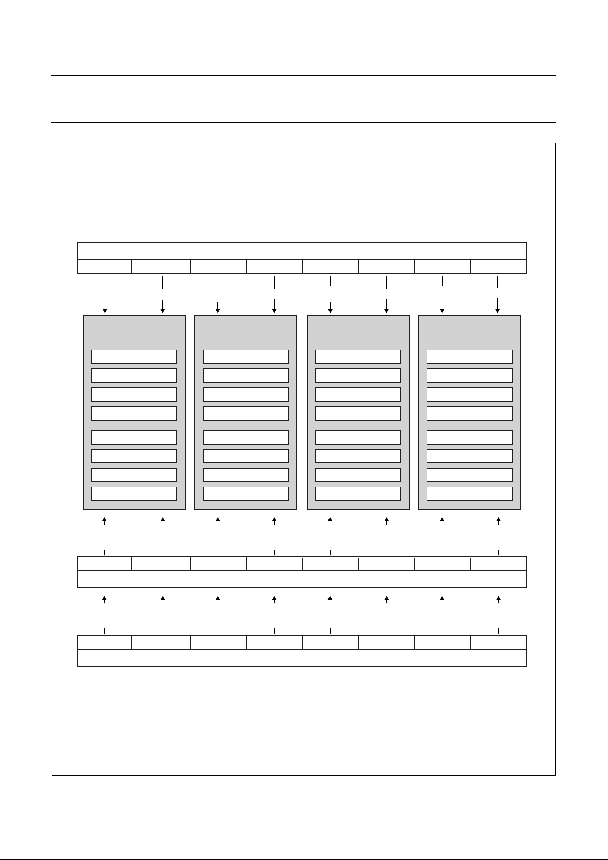
1999 Aug 19 48
Philips Semiconductors Objective Specification
Single-chip 8-bit microcontroller with CAN controller P8xC591
Fig.14 Acceptance Filter Tables.
handbook, full pagewidth
MHI014
ACCEPTANCE FILTER
BANK 4
ACR 0
MFORMATB4 AMODEB4 MFORMATB3 AMODEB3 MFORMATB2
ACCEPTANCE FILTER MODE REGISTER
AMODEB2 MFORMATB1 AMODEB1
B4F2EN B4F1EN B3F2EN B3F1EN B2F2EN
ACCEPTANCE FILTER ENABLE REGISTER
B2F1EN B1F2EN B1F1EN
dual/single
standard/
extended
ACR 1
ACR 2
ACR 3
AMR 0
AMR 1
AMR 2
AMR 3
ACCEPTANCE FILTER
BANK 3
ACR 0
ACR 1
ACR 2
ACR 3
AMR 0
AMR 1
AMR 2
AMR 3
ACCEPTANCE FILTER
BANK 2
ACR 0
ACR 1
ACR 2
ACR 3
AMR 0
AMR 1
AMR 2
AMR 3
ACCEPTANCE FILTER
BANK 1
ACR 0
ACR 1
ACR 2
ACR 3
AMR 0
AMR 1
AMR 2
AMR 3
dual/single
standard/
extended
dual/single
standard/
extended
dual/single
standard/
extended
filter 2
enable/
disable
filter 2
enable/
disable
filter 1
enable/
disable
filter 1
enable/
disable
filter 2
enable/
disable
filter 1
enable/
disable
filter 2
enable/
disable
filter 1
enable/
disable
B4F2PRIO B4F1PRIO B3F2PRIO B3F1PRIO B2F2PRIO
ACCEPTANCE FILTER PRIORITY REGISTER
B2F1PRIO B1F2PRIO B1F1PRIO
filter 2
priority
low/high
filter 2
priority
low/high
filter 1
priority
low/high
filter 1
priority
low/high
filter 2
priority
low/high
filter 1
priority
low/high
filter 2
priority
low/high
filter 1
priority
low/high
Page 49

1999 Aug 19 49
Philips Semiconductors Objective Specification
Single-chip 8-bit microcontroller with CAN controller P8xC591
12.5.17.1 Acceptance Filter Mode Register
The current operating mode is defined within the Acceptance Filter Mode Register located at CAN Address 29. A write
access to this register is possible only within Reset Mode (Mode Register).
Note, that some bits are implemented only in case of the corresponding acceptance filter bank is implemented.
Not implemented bits are read as “0”.
Table 31 Acceptance Filter Mode Register (ACF Mode) (CAN address 29)
7 6 5 4 3 2 1 0
MFORMATB4 AMODEB4 MFORMATB3 AMODEB3 MFORMATB2 AMODEB2 MFORMATB1 AMODEB1
Table 32 Acceptance Filter Mode Register (ACF Mode) 1 bits
BIT SYMBOL NAME VALUE FUNCTION
ACFMOD.7 MFORMATB4 Acceptance Filter
Format Bank 4
1 (EFF) Acceptance Filter Bank 4 is used for Extended Frame
Messages only, Standard Frame Messages are ignored
0 (SFF) Acceptance Filter Bank 4 is used for Standard Frame
Messages only, Extended Frame Messages are ignored
ACFMOD.6 AMODEB4 Acceptance Filter
Mode Bank 4
1 (single) The Single Acceptance Filter option is enabled for filter
bank 4, -> one long filter is active
0 (dual) The Dual Acceptance Filter option is enabled for filter
bank 4, -> two short filters are active
ACFMOD.5 MFORMATB3 Acceptance Filter
Format Bank 3
1 (EFF) Acceptance Filter Bank 3 is used for Extended Frame
Messages only, Standard Frame Messages are ignored
0 (SFF) Acceptance Filter Bank 3 is used for Standard Frame
Messages only, Extended Frame Messages are ignored
ACFMOD..4 AMODEB3 Acceptance Filter
Mode Bank 3
1 (single) The Single Acceptance Filter option is enabled for filter
bank 3, -> one long filter is active
0 (dual) The Dual Acceptance Filter option is enabled for filter
bank 3, -> two short filters are active
ACFMOD.3 MFORMATB2 Acceptance Filter
Format Bank 2
1 (EFF) Acceptance Filter Bank 2 is used for Extended Frame
Messages only , Standard Frame Messages are ignored.
0 (SFF) Acceptance Filter Bank 2 is used for Standard Frame
Messages only, Extended Frame Messages are
ignored.
ACFMOD.2 AMODEB2 Acceptance Filter
Mode Bank 2
1 (single) The Single Acceptance Filter option is enabled for filter
bank 2, -> one long filter is active
0 (dual) The Dual Acceptance Filter option is enabled for filter
bank 2, -> two short filters are active
ACFMOD.1 MFORMATB1 Acceptance Filter
Format Bank 1
1 (EFF) Acceptance Filter Bank 1 is used for Extended Frame
Messages only, Standard Frame Messages are ignored
0 (SFF) Acceptance Filter Bank 1 is used for Standard Frame
Messages only, Extended Frame Messages are ignored
ACFMOD.0 AMODEB1 Acceptance Filter
Mode Bank 1
1 (single) The Single Acceptance Filter option is enabled for filter
bank 1, -> one long filter is active
0 (dual) The Dual Acceptance Filter option is enabled for filter
bank 1, -> two short filters are active
Page 50

1999 Aug 19 50
Philips Semiconductors Objective Specification
Single-chip 8-bit microcontroller with CAN controller P8xC591
12.5.17.2 Acceptance Filter Enable Register
Each defined Acceptance Filter is enabled or disabled by a certain bit located within the Acceptance Filter Enable
Register. This allows to change the Acceptance Filter Contents “on the fly” during normal operation if the corresponding
filter is disabled previously. A disabled Acceptance Filter does not allow passing of messages to the receive buffer. If all
Acceptance Filters are disabled (default after hardware reset) no messages will pass to the receive buffer at all.
The Acceptance Code and Mask registers are writable only, if the related Acceptance Filter is disabled or the CAN Block
is in Reset Mode.
Note, that some bits are implemented only in case of the corresponding acceptance filter bank is implemented.
Not implemented bits are read as “0”.
Table 33 Acceptance Filter Enable Register (ACF Enable) (CAN address 30)
7 6 5 4 3 2 1 0
B4F2EN B4F1EN B3F2EN B3F1EN B2F2EN B2F1EN B1F2EN B1F1EN
Table 34 Acceptance Filter Enable Register (ACF Enable)
Note, if the Single Filter Mode is selected for an Acceptance Filter Bank, this single filter is related to the corresponding
Filter 1 Enable Bit. The Filter 2 Enable Bits have no influence within Single Filter Mode.
BIT SYMBOL NAME VALUE FUNCTION
ACFEN.7 B4F2EN Bank 4 Filter 2
Enable
1 (enabled) Filter 2 of Bank 4 is enabled, no write access to
corresponding Mask and Code Registers is possible
0 (disabled) Filter 2 of Bank 4 is enabled, changing of corresponding
Mask and Code Registers is possible.
ACFEN.6 B4F1EN Bank 4 Filter 1
Enable
1 (enabled) Filter 1 of Bank 4 is enabled, no write access to
corresponding Mask and Code Registers is possible
0 (disabled) Filter 1 of Bank 4 is enabled, changing of corresponding
Mask and Code Registers is possible.
ACFEN.5 B3F2EN Bank 3 Filter 2
Enable
1 (enabled) Filter 2 of Bank 3 is enabled, no write access to
corresponding Mask and Code Registers is possible
0 (disabled) Filter 2 of Bank 3 is enabled, changing of corresponding
Mask and Code Registers is possible.
ACFEN.4 B3F1EN Bank 3 Filter 1
Enable
1 (enabled) Filter 1 of Bank 3 is enabled, no write access to
corresponding Mask and Code Registers is possible
0 (disabled) Filter 1 of Bank 3 is enabled, changing of corresponding
Mask and Code Registers is possible.
ACFEN.3 B2F2EN Bank 2 Filter 2
Enable
1 (enabled) Filter 2 of Bank 2 is enabled, no write access to
corresponding Mask and Code Registers is possible
0 (disabled) Filter 2 of Bank 2 is enabled, changing of corresponding
Mask and Code Registers is possible.
ACFEN.2 B2F1EN Bank 2 Filter 1
Enable
1 (enabled) Filter 1 of Bank 2 is enabled, no write access to
corresponding Mask and Code Registers is possible
0 (disabled) Filter 1 of Bank 2 is enabled, changing of corresponding
Mask and Code Registers is possible.
ACFEN.1 B1F2EN Bank 1 Filter 2
Enable
1 (enabled) Filter 2 of Bank 1 is enabled, no write access to
corresponding Mask and Code Registers is possible
0 (disabled) Filter 2 of Bank 1 is enabled, changing of corresponding
Mask and Code Registers is possible.
ACFEN.0 B1F1EN Bank 1 Filter 1
Enable
1 (enabled) Filter 1 of Bank 1 is enabled, no write access to
corresponding Mask and Code Registers is possible
0 (disabled) Filter 1 of Bank 1 is enabled, changing of corresponding
Mask and Code Registers is possible.
Page 51

1999 Aug 19 51
Philips Semiconductors Objective Specification
Single-chip 8-bit microcontroller with CAN controller P8xC591
12.5.17.3 Acceptance Filter Priority Register
For each available Acceptance Filter it could be defined, whether a receive interrupt is forced immediately if a message
passes a certain Acceptance Filter or whether the programmed Receive Interrupt Level should be used for interruption.
This allows to use certain Acceptance Filters for alarm message recognition interrupting the host CPU immediately.
Note, that some bits are implemented only in case of the corresponding acceptance filter bank is implemented.
Not implemented bits are read as “0”.
Table 35 Acceptance Filter Priority Register (ACF Priority) (CAN address 31)
7 6 5 4 3 2 1 0
B4F2PRIO B4F1PRIO B3F2PRIO B3F1PRIO B2F2PRIO B2F1PRIO B1F2PRIO B1F1PRIO
Table 36 Acceptance Filter Priority Register (ACF Priority)
BIT SYMBOL NAME VALUE FUNCTION
ACFPRIO.7 B4F2PRIO Bank 4 Filter 2
Priority
1 (high) A receive interrupt is generated immediately, if a message
passes Filter 2 within Acceptance Filter Bank 4
0 (low) A receive interrupt is generated, if the FIFO level exceeds
the Receive Interrupt Level Register.
ACFPRIO.6 B4F1PRIO Bank 4 Filter 1
Priority
1 (high) A receive interrupt is generated immediately, if a message
passes Filter 1 within Acceptance Filter Bank 4
0 (low) A receive interrupt is generated, if the FIFO level exceeds
the Receive Interrupt Level Register.
ACFPRIO.5 B3F2PRIO Bank 3 Filter 2
Priority
1 (high) A receive interrupt is generated immediately, if a message
passes Filter 2 within Acceptance Filter Bank 3
0 (low) A receive interrupt is generated, if the FIFO level exceeds
the Receive Interrupt Level Register.
ACFPRIO.4 B3F1PRIO Bank 3 Filter 1
Priority
1 (high) A receive interrupt is generated immediately, if a message
passes Filter 1 within Acceptance Filter Bank 3
0 (low) A receive interrupt is generated, if the FIFO level exceeds
the Receive Interrupt Level Register.
ACFPRIO.3 B2F2PRIO Bank 2Filter 2
Priority
1 (high) A receive interrupt is generated immediately, if a message
passes Filter 2 within Acceptance Filter Bank 2
0 (low) A receive interrupt is generated, if the FIFO level exceeds
the Receive Interrupt Level Register.
ACFPRIO.2 B2F1PRIO Bank 2 Filter 1
Priority
1 (high) A receive interrupt is generated immediately, if a message
passes Filter 1 within Acceptance Filter Bank 2
0 (low) A receive interrupt is generated, if the FIFO level exceeds
the Receive Interrupt Level Register.
ACFPRIO.1 B1F2PRIO Bank 1 Filter 2
Priority
1 (high) A receive interrupt is generated immediately, if a message
passes Filter 2 within Acceptance Filter Bank 1
0 (low) A receive interrupt is generated, if the FIFO level exceeds
the Receive Interrupt Level Register.
ACFPRIO.0 B1F1PRIO Bank 1 Filter 1
Priority
1 (high) A receive interrupt is generated immediately, if a message
passes Filter 1 within Acceptance Filter Bank 1
0 (low) A receive interrupt is generated, if the FIFO level exceeds
the Receive Interrupt Level Register.
Page 52

1999 Aug 19 52
Philips Semiconductors Objective Specification
Single-chip 8-bit microcontroller with CAN controller P8xC591
12.5.17.4 Single Filter Configuration
In this filter configuration one long filter (4-byte) could be
defined. The bit correspondences between the filter bytes
and the Message bytes depends on the programmed
Frame Format (see ACF Mode Register).
Single Filter Standard Frame:
If the Standard Frame Format is selected, the complete
Identifier including the RTR bit and the first two data bytes
are used for acceptance filtering. Messages may also be
accepted if there are no data bytes existing due to a set
RTR bit or if there is no or only one data byte because of
the corresponding data length code.
For a successful reception of a message, all single bit
comparisons have to signal acceptance. Note that the 4
least significant bits of AMR1 and ACR1 are not used. In
order to keep compatible with future products these bits
should be programmed to be “don‘t care” by setting
AMR1.3, AMR1.2, AMR1.1 and AMR1.0 to “1”.
Fig.15 Single Filter Configuration, receiving Standard Frame Messages.
handbook, full pagewidth
Addr.: 16 ACR0
7
6 5 4 3 2 10
MSB LSB
Addr.: 18 ACR2
7
6 5 4 3 2 10
MSB LSB
Addr.: 19 ACR3
7
6 5 4 3 2 10
MSB LSB
Addr.: 17 ACR1
7
6 5 4 3 2 10
MSB LSB
unused
Addr.: 20 AMR0
7
6 5 4 3 2 10
ID.28
ID.27
ID.26
ID.25
ID.24
ID.23
ID.22
MSB LSB
Addr.: 22 AMR2
7
6 5 4 3 2 10
MSB LSB
Addr.: 23 AMR3
7
6 5 4 3 2 10
MSB LSB
Addr.: 21 AMR1
7
6 5 4 3 2 10
MSB LSB
unused
ID.21
DB1.7
DB1.6
DB1.5
DB1.4
DB1.3
DB1.2
DB1.1
DB1.0
DB2.7
DB2.6
DB2.5
DB2.4
DB2.3
DB2.2
DB2.1
DB2.0
ID.20
ID.19
ID.18
RTR
&
[6]
[7]
0 1 not accepted
accepted
≥1
[0]
=
Message Bit
Acceptance Code Bit
Acceptance Mask Bit
DBx.y = Data Byte x, Bit y
MHI015
Page 53

1999 Aug 19 53
Philips Semiconductors Objective Specification
Single-chip 8-bit microcontroller with CAN controller P8xC591
Single Filter Extended Frame:
If the Extended Frame Format is selected, the complete
Identifier including the RTR bit is used for acceptance
filtering.
For a successful reception of a message, all single bit
comparisons have to signal acceptance. Note that the 2
least significant bits of AMR3 and ACR3 are not used. In
order to keep compatible with future products these bits
should be programmed to be “don‘t care” by setting
AMR3.1 and AMR3.0 to “1”.
Fig.16 Single Filter Configuration, receiving Extended Frame Messages.
handbook, full pagewidth
Addr.: 16 ACR0
7
6 5 4 3 2 10
MSB LSB
Addr.: 18 ACR2
7
6 5 4 3 2 10
MSB LSB
Addr.: 19 ACR3
7
6 5 4 3 2 10
MSB LSB
Addr.: 17 ACR1
7
6 5 4 3 2 10
MSB LSB
unused
Addr.: 20 AMR0
7
6 5 4 3 2 10
ID.28
ID.27
ID.26
ID.25
ID.24
ID.23
ID.22
MSB LSB
Addr.: 22 AMR2
7
6 5 4 3 2 10
MSB LSB
Addr.: 23 AMR3
7
6 5 4 3 2 10
MSB LSB
Addr.: 21 AMR1
7
6 5 4 3 2 10
MSB LSB
unused
ID.21
ID.20
ID.19
ID.18
ID.17
ID.16
ID.15
ID.14
ID.13
ID.12
ID.11
ID.10
ID.9
ID.8
ID.7
ID.6
ID.5
ID.2
ID.3
ID.4
ID.1
ID.0
RTR
&
[6]
[7]
0 1 not accepted
accepted
≥1
[0]
=
Message Bit
Acceptance Code Bit
Acceptance Mask Bit
MHI016
Page 54
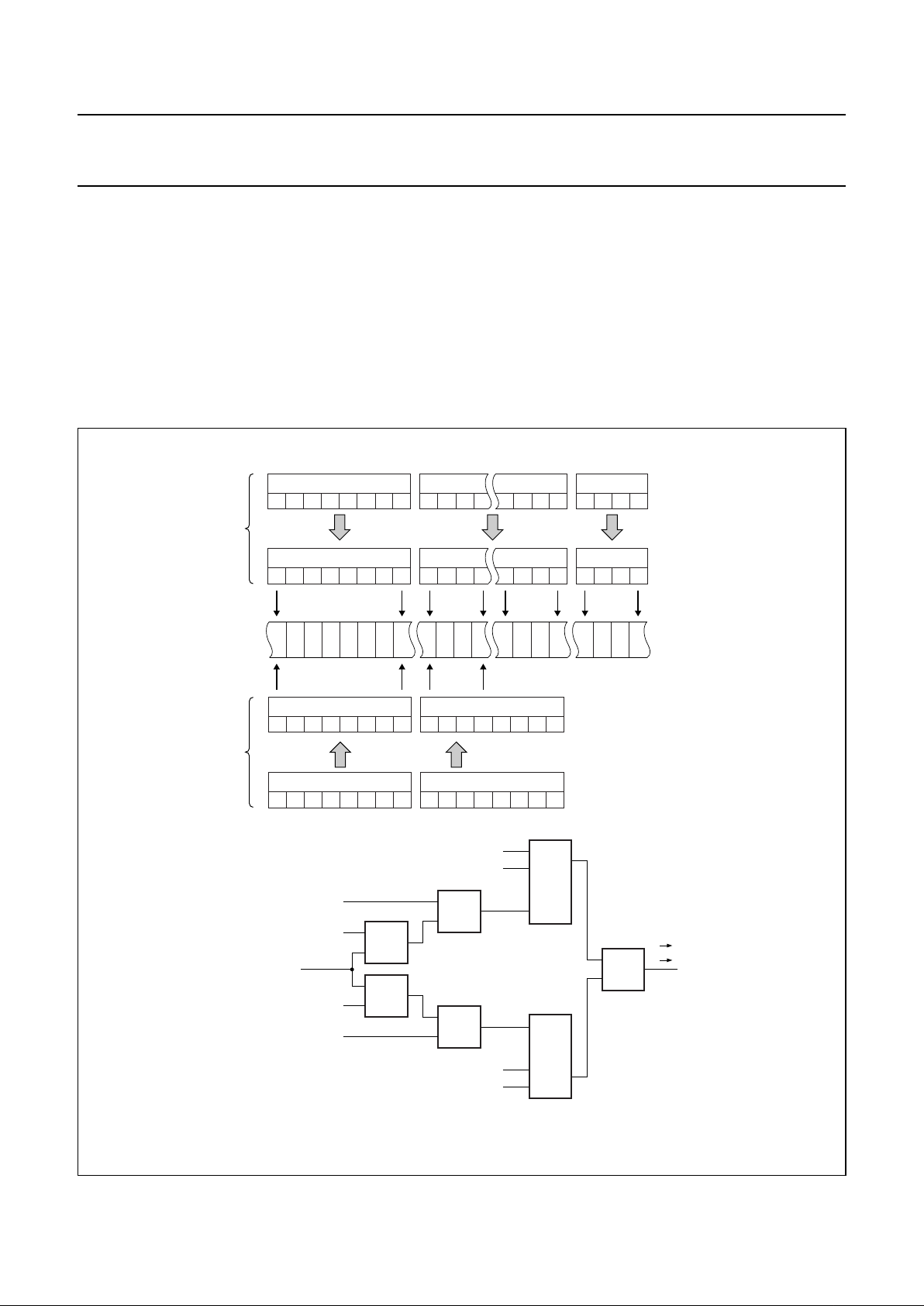
1999 Aug 19 54
Philips Semiconductors Objective Specification
Single-chip 8-bit microcontroller with CAN controller P8xC591
12.5.17.5 Dual Filter Configuration
In this filter configuration two short filters could be defined.
A received message is compared with both filters to
decide, whether this message should be copied into the
Receive Buffer or not. If at least one of the filters signals an
acceptance, the received message becomes valid. The bit
correspondences between the filter bytes and the
message bytes depends on the currently received Frame
Format.
Dual Filter Standard Frame:
If the Standard Frame Format is selected, the two defined
filters are different. The first filter compares the complete
Standard Identifier including the RTR bit and the first Data
Byte of the message. The second filter just compares the
complete Standard Identifier including the RTR bit.
Fig.17 Dual Filter Configuration, receiving Standard Frame Messages.
handbook, full pagewidth
Addr.: 16 ACR0
7
6 5 4 3 2 10
MSB LSB
ACR1
3 2 10
LSB
ACR3
3 2 10
LSB
Addr.: 17
7
6 54
MSB
ID.28
ID.27
ID.26
ID.25
ID.24
ID.23
ID.22
ID.21
ID.20
ID.19
ID.18
RTR
DB1.7
DB1.6
DB1.5
DB1.4
DB1.1
DB1.2
DB1.3
DB1.0
Addr.: 20 AMR0
7
6 5 4 3 2 10
MSB LSB
AMR1
3 2 10
LSB
AMR3
3 2 10
LSB
Addr.: 21
7
6 54
MSB
[6]
[7]
≥1
≥1
[0]
[0]
≥1
=
Acceptance Code Bit
Acceptance Mask Bit
Filter 1
Filter 2
Filter 1
Filter 2
Message
Addr.: 22 AMR2
7
6 5 4 3 2 10
MSB LSB
Addr.: 23 AMR3
7
6 5 4
MSB
Addr.: 18 ACR2
7
6 5 4 3 2 10
MSB LSB
Addr.: 19 ACR3
7
6 5 4
MSB
. . .
. . .
. . .
.
.
.
[6]
[7]
0
1
not accepted
accepted
=
Message Bit
Acceptance Code Bit
Acceptance Mask Bit
. . .
. . .
. . .
.
.
.
&
&
MHI017
Page 55
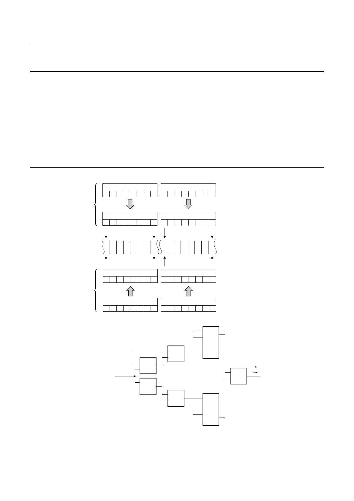
1999 Aug 19 55
Philips Semiconductors Objective Specification
Single-chip 8-bit microcontroller with CAN controller P8xC591
For a successful reception of a message, all single bit
comparisons of at least one complete filter have to signal
acceptance. In case of a set RTR bit or a data length code
of “0” no data byte is existing. Nevertheless, a message
may pass Filter 1, if the first part up to the RTR bit signals
acceptance.
If no data byte filtering is required for Filter 1, the four least
significant bits of AMR1 and AMR3 have to be set “1”
(don‘t care). Then both filters are working identically using
the standard identifier range including the RTR bit.
Dual Filter Extended Frame:
If the Extended Frame Format is selected, the two defined
filters are looking identically. Both filters are comparing the
first two bytes of the Extended Identifier range only.
For a successful reception of a message, all single bit
comparisons of at least one complete filter have to signal
acceptance.
Fig.18 Dual Filter Configuration, receiving Extended Frame Messages.
handbook, full pagewidth
Addr.: 16 ACR0
7
6 5 4 3 2 10
MSB LSB
ID.28
ID.27
ID.26
ID.25
ID.24
ID.23
ID.22
ID.21
ID.20
ID.19
ID.18
ID.17
ID.16
ID.15
ID.14
ID.13
Addr.: 20 AMR0
7
6 5 4 3 2 10
MSB LSB
[6]
[7]
≥1
≥1
[0]
[0]
≥1
=
Acceptance Code Bit
Acceptance Mask Bit
Filter 1
Filter 2
Filter 1
Filter 2
Message
Addr.: 22 AMR2
7
6 5 4 3 2 10
MSB LSB
Addr.: 23 AMR3
Addr.: 18 ACR2
7 6 5 4 3 2 10
76543210
76543210
MSB LSB
MSB LSB
MSB LSB
Addr.: 19 ACR3
. . .
. . .
. . .
.
.
.
[6]
[7]
0
1
not accepted
accepted
=
Message Bit
Acceptance Code Bit
Acceptance Mask Bit
. . .
. . .
. . .
.
.
.
&
&
MHI018
Addr.: 17 ACR1
67 5 4 3 2 10
MSB LSB
Addr.: 21 AMR1
67 5 4 3 2 10
MSB LSB
Page 56

1999 Aug 19 56
Philips Semiconductors Objective Specification
Single-chip 8-bit microcontroller with CAN controller P8xC591
12.5.18 TRANSMIT BUFFER
The global layout of the Transmit Buffer is shown in Fig.19.
One has to distinguish between the Standard Frame
Format (SFF) and the Extended Frame Format (EFF)
configuration. The transmit buffer allows the definition of
one transmit message with up to eight data bytes.
12.5.18.1 Transmit Buffer Layout
It is subdivided into Descriptor and Data Field where the
first byte of the Descriptor Field is the Frame Information
Byte (Frame Info). It describes the Frame Format (SFF or
EFF), Remote or Data Frame and the Data Length. Two
identifier bytes for SFF and four bytes for EFF messages
follow. The Data Field contains up to eight data bytes. The
Transmit Buffer has a length of 13 bytes and is located in
the CAN address range from 112 to 124.
Fig.19 Transmit Buffer Layout for Standard and Extended Frame Format configurations.
handbook, full pagewidth
MHI023
TX Frame information
Standard Frame Format (SFF)
112CAN Address
TX Identifier 1113
TX Identifier 2114
TX Data byte 1115
TX Data byte 2116
TX Data byte 3117
TX Data byte 4118
TX Data byte 5119
TX Data byte 6120
TX Data byte 7121
TX Data byte 8122
unused123
unused124
TX Frame information
Extended Frame Format (EFF)
112CAN Address
TX Identifier 1113
TX Identifier 2114
TX Identifier 3115
TX Identifier 4116
TX Data byte 1117
TX Data byte 2118
TX Data byte 3119
TX Data byte 4120
TX Data byte 5121
TX Data byte 6122
TX Data byte 7123
TX Data byte 8124
Page 57

1999 Aug 19 57
Philips Semiconductors Objective Specification
Single-chip 8-bit microcontroller with CAN controller P8xC591
12.5.18.2 Descriptor Field of the Transmit Buffer
This configuration is chosen to be compatible with the Receive Buffer Layout (see Section 12.5.19.1).
The values marked with “( )” in the Transmit Buffer should be set to the values expected in the Receive Buffer for an easy
comparison, only when using the Self Reception facility, otherwise they are don’t care.
Table 37 Frame Format (FF) and Remote Transmission Request (RTR) bits
BIT VALUE FUNCTION
FF 1 (EFF) Extended Frame Format will be transmitted by the CAN Controller
0 (SFF) Standard Frame Format will be transmitted by the CAN Controller
RTR 1 (remote) Remote Frame will be transmitted by the CAN Controller
0 (data) Data Frame will be transmitted by the CAN Controller
Fig.20 Bit Layout Transmit Buffer.
7
FF
6
RTR5(0)4(0)3DLC.32DLC.21DLC.10DLC.0
6
RTR5(0)4(0)3DLC.32DLC.21DLC.10DLC.0
Addr. 112 TX Frame Information Addr. 112 TX Frame Information
Standard Frame Format (SFF) Extended Frame Format (EFF)
7
ID.286ID.275ID.264ID.253ID.242ID.231ID.220ID.21
Addr 113 TX Identifier 1
7
ID.206ID.195ID.184(RTR)3(0)2(0)1(0)0(0)
Addr. 114 TX Identifier 2
7
ID.286ID.275ID.264ID.253ID.242ID.231ID.220ID.21
Addr. 113 TX Identifier 1
7
ID.206ID.195ID.184ID.173ID.162ID.151ID.140ID.13
Addr. 114 TX Identifier 2
7
ID.126ID.115ID.104ID.93ID.82ID.71ID.60ID.5
Addr. 115 TX Identifier 3
7
ID.46ID.35ID.24ID.13ID.02(RTR)1(0)0(0)
Addr. 116 TX Identifier 4
Meaning of the Transmit Buffer Bits:
ID.x Identifier bit x
FF Frame Format
RTR Remote Transmission Request
DLC.x Data Length Code bit x
X don’t care
0 don’t care, but recommended to be
compatible to Receive Buffer
7
FF
Page 58

1999 Aug 19 58
Philips Semiconductors Objective Specification
Single-chip 8-bit microcontroller with CAN controller P8xC591
12.5.18.3 Data Length Code (DLC)
The number of bytes in the Data Field of a message is
coded by the Data Length Code. At the start of a Remote
Frame transmission the Data Length Code is not
considered due to the RTR bit being ‘1’ (remote). This
forces the number of transmitted/received data bytes to be
0. Nevertheless, the Data Length Code must be specified
correctly to avoid bus errors, if two CAN Controllers start a
Remote Frame transmission with the same identifier
simultaneously.
The range of the Data Byte Count is 0 to 8 bytes and is
coded as follows:
`
For reasons of compatibility no Data Length Code > 8
should be used. If a value greater than 8 is selected, 8
bytes are transmitted in the data frame with the Data
Length Code specified in DLC.
12.5.18.4 Identifier (ID)
In Standard Frame Format (SFF) the Identifier consists of
11 bits (ID.28 to ID.18) and in Extended Frame Format
(EFF) messages the identifier consists of 29 bits (ID.28 to
ID.0). ID.28 is the most significant bit, which is transmitted
first on the bus during the arbitration process. The
Identifier acts as the message’s name, used in a receiver
for acceptance filtering, and also determines the bus
access priority during the arbitration process. The lower
the binary value of the Identifier the higher the priority. This
is due to the larger number of leading dominant bits during
arbitration.
12.5.18.5 Data Field
The number of transferred data bytes is defined by the
Data Length Code. The first bit transmitted is the most
significant bit of data byte 1 at address 115 (SFF) or
address 117 (EFF).
DataByteCount 8 DLC.3 4 DLC.2 2 DLC.1 DLC.0
+×+×+×=
Page 59
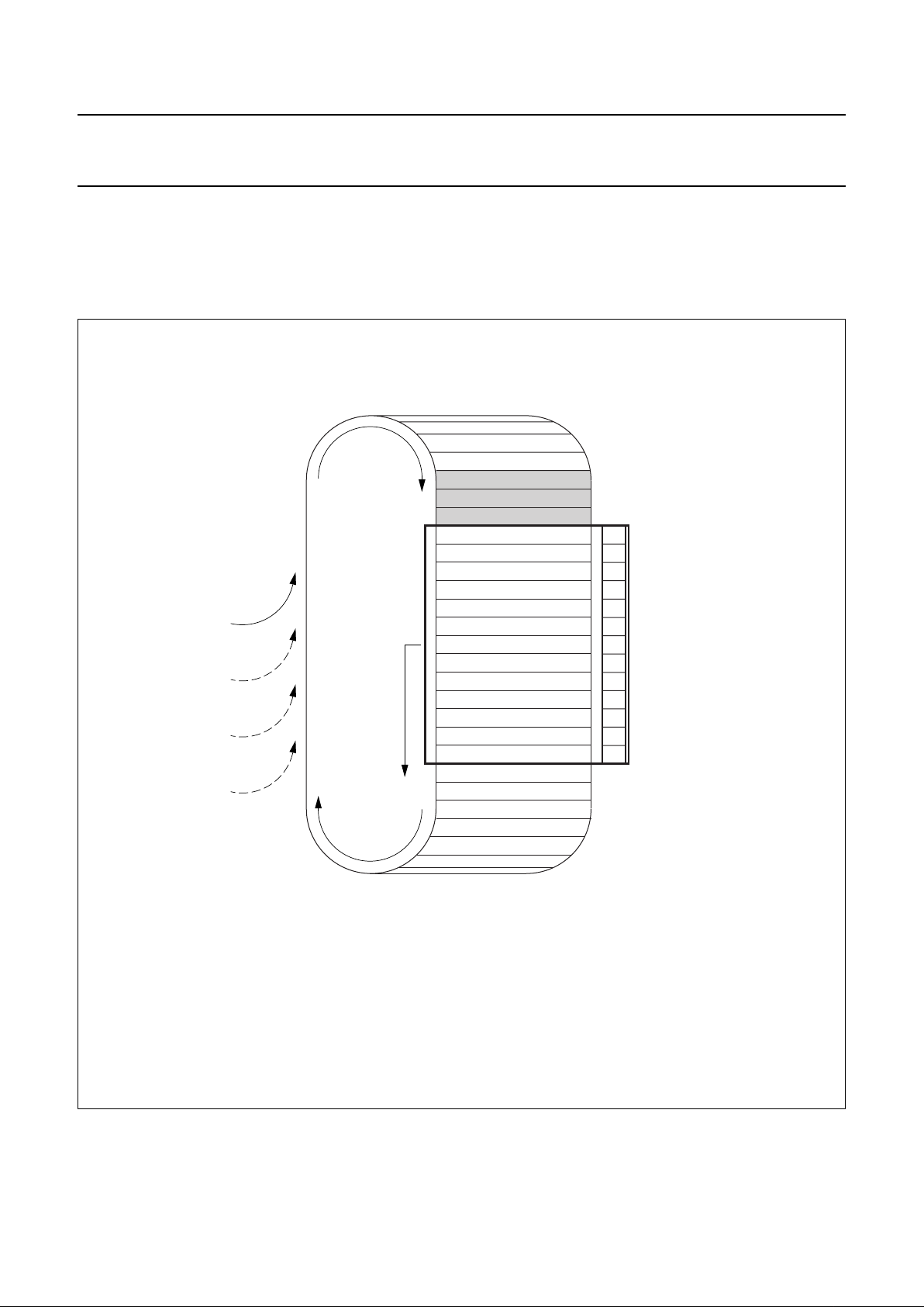
1999 Aug 19 59
Philips Semiconductors Objective Specification
Single-chip 8-bit microcontroller with CAN controller P8xC591
12.5.19 RECEIVE BUFFER
The global layout of the Receive Buffer is very similar to the Transmit Buffer described in the previous chapter. The
Receive Buffer is the accessible part of the RXFIFO and is located in the range between CAN Address 96 and 108. Each
message is subdivided into a Descriptor and a Data Field.
Fig.21 Example of the message storage within the RXFIFO.
Message 1 is now available in the Receive Buffer
Note that message 2 should not be read until it has been shifted to address 96 by a Release Receive
Buffer Command because this message may be in process now and due to this not fixed.
handbook, full pagewidth
MHI019
message 3
message 2
message 1
receive
buffer
window
incoming
messages
receive
FIFO
106
107
108
103
104
105
100
101
102
99
96
97
98
Page 60
1999 Aug 19 60
Philips Semiconductors Objective Specification
Single-chip 8-bit microcontroller with CAN controller P8xC591
12.5.19.1 Descriptor File of the Receive Buffer
Identifier, Frame Format, Remote Transmission Request bit and Data Length Code have the same meaning as described
in the Transmit Buffer.
Fig.22 Bit Layout Receive Buffer.
7
ID.28
6
ID.275ID.264ID.253ID.242ID.231ID.220ID.21
7
ID.28
6
ID.275ID.264ID.253ID.242ID.231ID.220ID.21
Addr. 97 RX Identifier 1 Addr. 97 RX Identifier 1
Standard Frame Format (SFF) Extended Frame Format (EFF)
7
ID.206ID.195ID.184RTR30
2
0
1
0
0
0
Addr. 98 RX Identifier 2
7
ID.206ID.195ID.184ID.173ID.162ID.151ID.140ID.13
Addr. 98 RX Identifier 2
7
ID.126ID.115ID.104ID.93ID.82ID.71ID.60ID.5
Addr. 99 RX Identifier 3
7
ID.46ID.35ID.24ID.13ID.02RTR10
0
0
Addr. 100 RX Identifier 4
Meaning of the Receive Buffer Bits:
ID.x Identifier bit x
IDX.x Index bit x
FF Frame Format
RTR Remote Transmission Request
DLC.x Data Length Code bit x
7
FF6RTR50
4
03DLC.32DLC.21DLC.10DLC.0
Addr. 96 RX Frame Information
7
FF6RTR50
4
03DLC.32DLC.21DLC.10DLC.0
Addr. 96 RX Frame Information
Note:
The received Data Length Code located in the Frame
Information Byte represents the real sent Data Length
Code, which may be greater than 8 (depends on
transmitting CAN node). Nevertheless, the maximum
number of received data bytes is 8. This should be taken
into account by reading a message from the Receive
Buffer.
It depends on the data length how many CAN messages
can fit in the RXFIFO at one time. If there is not enough
space for a new message within the RXFIFO, the CAN
Controller generates a Data Overrun condition the
moment this message becomes valid and the acceptance
test was positive. A message that is partly written into the
RXFIFO, when the Data Overrun situation occurs, is
deleted. This situation is signalled to the CPU via the
Status Register and the Data Overrun Interrupt, if enabled.
Page 61

1999 Aug 19 61
Philips Semiconductors Objective Specification
Single-chip 8-bit microcontroller with CAN controller P8xC591
13 SERIAL I/O
The P8xC591 is equipped with three independent serial
ports: CAN, SIO0 and SIO1. SIO0 is a Standard Serial
Interface UART with enhanced functionality. In following
there will be one Section describing the Standard UART
functionality and an extra Section for Enhanced UART.
SIO1 accommodates the I2C bus.
14 SIO0 STANDARD SERIAL INTERFACE UART
The serial port is full duplex, meaning it can transmit and
receive simultaneously. It is also receive-buffered,
meaning it can commence reception of a second byte
before a previously received byte has been read from the
register. (However, if the first byte still hasn’t been read by
the time reception of the second byte is complete, one of
the bytes will be lost.) The serial port receive and transmit
registers are both accessed at Special Function Register
transmit registers are both accessed at Special Function
Register S0BUF. Writing to S0BUF loads the transmit
register, and reading S0BUF accesses a physically
separate receive register.
The serial port can operate in 4 modes (one synchronous
mode, three asynchronous modes). The baud rate clock
for the serial port is derived from the oscillator frequency
(mode 0, 2) or generated either by timer 1 or by dedicated
baud rate generator (mode 1, 3).
Mode 0 Shift Register (Synchronous) Mode:
Serial data enters and exits through RxD. TxD
outputs the shift clock. 8 bits are transmitted/
received (LSB first). The baud rate is fixed1⁄6the
oscillator frequency.
Mode 1 8-bit UART, Variable Baud Rate:
10 bits are transmitted (through TxD) or received
(through RxD): a start bit (0), 8 data bits (LSB
first), and a stop bit (1). On receive, the stop bit
goes into RB8 in Special Function Register
SCON. The baud rate is variable.
Mode 2 9-bit UART, Fixed Baud Rate:
11 bits are transmitted (through TxD) or received
(through RxD): start bit (0), 8 data bits (LSB first),
a programmable 9th data bit, and a stop bit (1).
On Transmit, the 9th data bit (TB8 in SCON) can
be assigned the value of 0 or 1. Or, for example,
the parity bit (P, in the PSW) could be moved into
TB8. On receive, the 9th data bit goes into RB8 in
Special Function Register SCON, while the stop
bit ignored. The baud rate is programmable to
either1⁄16 or1⁄32 the oscillator frequency.
Mode 3 9-bit UART, Variable Baud Rate:
11 bits are transmitted (through TxD) or received
(through RxD): start bit (0), 8 data bits (LSB first),
a programmable 9th data bit, and a stop bit (1). In
fact, Mode 3 is the same as Mode 2 in all respects
except baud rate. The baud rate in Mode 3 is
variable.
In all four modes, transmission is initiated by any
instruction that uses S0BUF as a destination register.
Reception is initiated in Mode 0 by the condition RI = 0 and
REN = 1. Reception is initiated in the other modes by the
incoming start bit if REN = 1.
14.1 Multiprocessor Communications
Modes 2 and 3 have a special provision for multiprocessor
communications. In these modes, 9 data bits are received.
The 9th one goes into RB8. Then comes a stop bit. The
port can be programmed such that when the stop bit is
received, the serial port interrupt will be activated only if
RB8 = 1. This feature is enabled by setting bit SM2 in
SCON. A way to use this feature in multiprocessor
systems is as follows:
When the master processor wants to transmit a block of
data to one of several slaves, it first send out an address
byte which indentifies the target slave. An address byte
differs from a data byte in that the 9th bit is 1 in an address
byte and 0 in a data byte. With SM2 = 1, no slave will be
interrupted by a data byte. An address byte, however, will
interrupt all slaves, so that each slave can examine the
received byte and see if it is being addressed. The
addressed slave will clear its SM2 bit and prepare to
receive the data bytes that will be coming. The slaves that
weren’t being addressed leave their SM2s set and go on
about their business, ignoring the coming data bytes.
SM2 has no effect in Mode 0, and in Mode 1 can be used
to check the validity of the stop bit. In a Mode 1 reception,
if SM2 = 1, the receive interrupt will not be activated unless
a valid stop bit is received.
14.2 Serial Port Control Register
The serial port control and status register is the Special
Function Register SCON, shown in Table 38, 40 and 41.
This register contains not only the mode selection bits, but
also the 9th data bit for transmit and receive (TB8 and
RB8), and the serial port interrupt bits (TI and RI).
S0BUF is the receive and transmit buffer of serial
interface. Writing to S0BUF loads the transmit register and
initiates transmission. Reading out S0BUF accesses a
physically separate receive register.
Page 62

1999 Aug 19 62
Philips Semiconductors Objective Specification
Single-chip 8-bit microcontroller with CAN controller P8xC591
14.3 Baud Rate Generation
There are several possibilities to generate the baud rate
clock for the serial port depending on the mode in which it
is operating.
For clarification some terms regarding the difference
between “baud rate clock” and “baud rate” should be
mentioned. The serial interface requires a clock rate which
is 16 times the baud rate for internal synchronization.
Therefore, the baud rate generators have to provide a
“baud rate clock” to the serial interface which - there
divided by 16 - results in the actual “baud rate”. However,
all formulas given in the following section already include
the factor and calculate the final baud rate. Further, the
abbreviation f
CLK
refers to the external clock frequency
(oscillator or external input clock operation).
The baud rate of the serial port is controlled by the two bits
SPS and SMOD1 which are located in the Special
Function Registers S0PSH and PCON. In SFRs S0PSH
and S0PSL the prescaler load value of the internal baud
rate generator can be programmed (see Table 38 to 43).
14.3.1 I
NTERNAL BAUD RATE GENERATOR PRESCALER S0PSH, S0PSL
Table 38 Internal Baud Rate Generator Prescaler Low Register S0PSL (address FAH)
Prescaler load value
Table 39 Description of S0PSL bits
Table 40 Internal Baud Rate Generator Prescaler High Register S0PSH (address FBH)
Prescaler higher nibble load value
Table 41 Description of S0PSH bits
14.3.2 PCON
FOR THE INTERNAL BAUD RATE GENERATOR
Table 42 PCON (address 87H)
Prescaler load value
Table 43 Description of SMOD1 and SMOD0 bits
76543210
prescaler load value
BIT SYMBOL DESCRIPTION
7 to 0 − Baud reload low value. Lower 8 bits of the baud rate timer reload value.
76543210
SPS −−− higher nibble load value
BIT SYMBOL DESCRIPTION
7 SPS Baud rate generator enable. When set, the baud rate of serial interface is derived from
the dedicated baud rate generator. When cleared (default after reset), baud rate is derived
from the Timer 1 overflow rate.
6 to 4 − Reserved.
3 to 0 − Baud rate generator reload high value. Upper four bits of the baud rate timer value.
76543210
SMOD1 SMOD0 (POF) (WLE) (GF1) (GF0) (PD) (IDL)
BIT SYMBOL DESCRIPTION
7 SMOD1 Double Baud rate. When set, the baud rate of serial interface is modes 1, 2, 3 is
doubled. After reset this bit is cleared.
6 SMOD0 Double Baud rate. Selects SM0/FE for SCON.7 bit.
5 to 0 (POF) to (IDL) Description refer to Section 11.3.5“Power Control Register (PCON)”.
Page 63
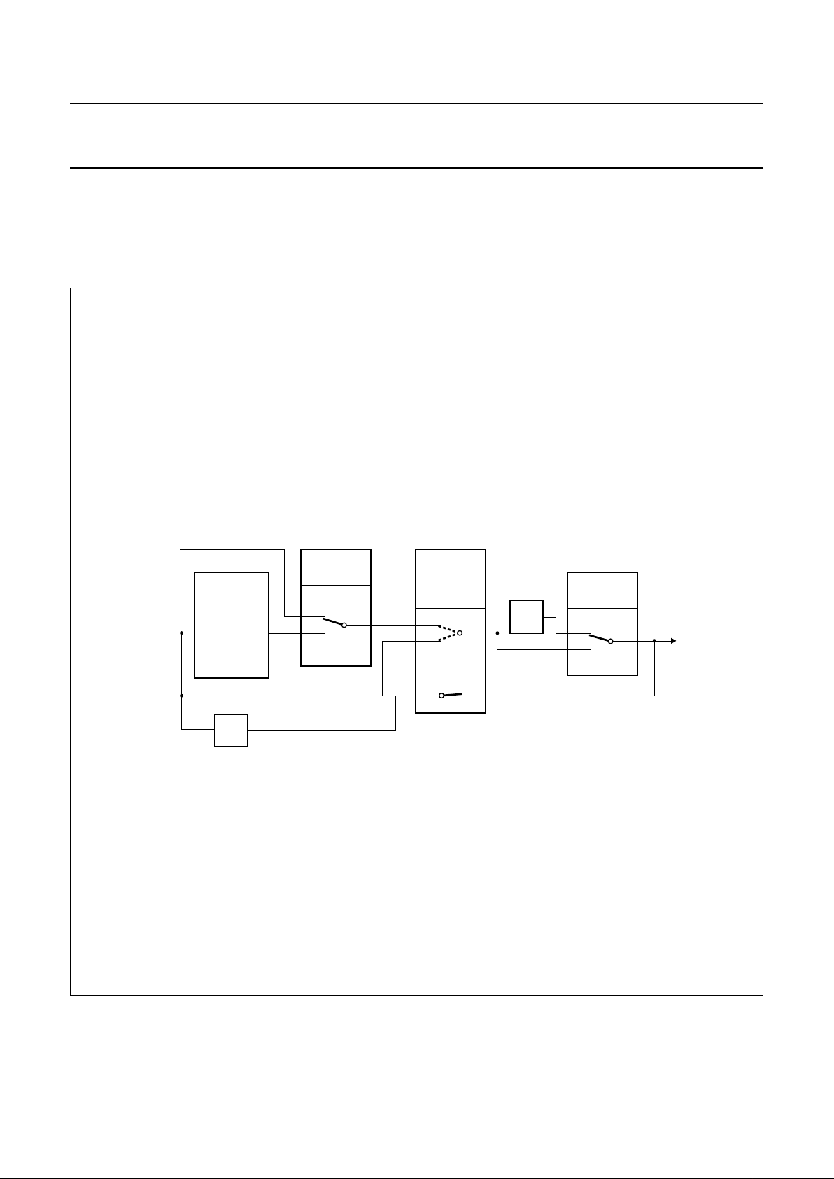
1999 Aug 19 63
Philips Semiconductors Objective Specification
Single-chip 8-bit microcontroller with CAN controller P8xC591
14.3.3 BAUD RATE GENERATION OVERVIEW OF OPTIONS
Depending on the programmed operating mode different paths are selected for the baud rate clock generation. Figure 23
shows the dependencies of the serial port baud rate clock generation on the two control bits and from the mode which
is selected in the Special Function Register SCON:
Fig.23 Baud Rate Generation for the Serial Port.
Note: The switch configuration shows the reset state.
handbook, full pagewidth
MHI024
BAUD
RATE
GENERATOR
BAUD
RATE
CLOCK
÷6
(S0PSH
S0PSL)
S0PSH.7
(SPS)
TIMER 1
overflow
f
CLK
SCON.7
SCON.6
(SM0/FE)
mode 1
mode 3
only one
mode can be selected
mode 2
mode 0
0
1
PCON.7
(SMOD1)
0
1
÷2
Page 64
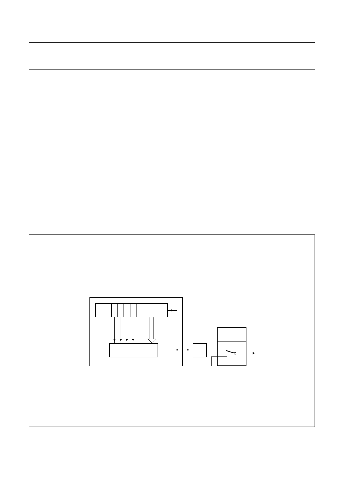
1999 Aug 19 64
Philips Semiconductors Objective Specification
Single-chip 8-bit microcontroller with CAN controller P8xC591
14.3.4 BAUD RATE IN MODE 0
The baud rate in Mode 0 is fixed to:
14.3.5 BAUD RATE IN MODE 2
The baud rate in Mode 2 depends on the value of bit
SMOD1 in Special Function Register PCON. If SMOD1 =
0 (which is the value after reset), the baud rate is
1
⁄32 of
oscillator frequency. If SMOD1 = 1, the baud rate is
1
⁄16 of
the oscillator frequency:
14.3.6 B
AUD RATE IN MODE 1 AND 3
In these modes the baud rate is variable and can be
generated alternatively by a baud rate generator or by
Timer 1.
Mode 0 baud rate
oscillator frequency
6
-------------------------------------------------------
=
Mode 2 baud rate
2
SMO
D1
32
--------------------
oscillator frequency×=
14.3.7 USING THE INTERNAL BAUD RATE GENERATOR
In Modes 1 and 3, the P8xC591 can use an internal baud
rate generator for the serial port. To enable this feature, bit
SPS (bit 7 of Special Function Register S0PSH) must be
set. Bit SMOD1 (PCON.7) controls a divide-by-2 circuit
which affect the input and output clock signal of the baud
rate generator. After reset the divide-by-2 circuit is active
and the resulting overflow output clock will be divided by 2.
The input clock of the baud rate generator is f
CLK.
The baud rate generator consists of its own free running
upward counting 12-bit timer. On overflow of this timer
(next count step after counter value FFFH) there is an
automatic 12-bit reload from the registers S0PSL and
S0PSH. The lower 8 bits of the timer are reloaded from
S0PSL, while the upper four bits are reloaded from bit 0 to
3 of register S0PSH. The baud rate timer is reloaded by
writing to S0PSH.
Fig.24 Serial Port Input Clock when using the Baud Rate Generator.
Note: The switch configuration shows the reset state.
handbook, full pagewidth
MHI025
BAUD
RATE
CLOCK
BAUD RATE
f
CLK
PCON.7
(SMOD1)
0
1
÷212 BIT TIMER
S0PSH S0PSL
overflow
input
clock
.3
.2 .1 .0
Page 65

1999 Aug 19 65
Philips Semiconductors Objective Specification
Single-chip 8-bit microcontroller with CAN controller P8xC591
With the baud rate generator as clock source for the serial
port in Mode 1 and Mode 3, the baud rate of can be
determined as follows:
Mode 1, 3 baud rate =
Baud rate generator overflow rate =
2
12
- S0PS with S0PS = S0PSH.3 - 0, S0PSL.7 - 0.
S0PS: Baud Rate Generator Prescaler load value
Table 47 lists baud rates and how they can be obtained
from the Internal Baud Rate Generator.
14.3.8 USING TIMER 1 TO GENERATE BAUD RATES
In Mode 1 and 3 of the serial port also timer 1 can be used
for generating baud rates. Then the baud rate is
determined by the timer 1 overflow rate and the value of
SMOD1 as follows:
2
SMOD1
osciillator frequency×
32 (baud rate generator overflow rate)×
---------------------------------------------------------------------------------------------------------
The Timer 1 interrupt is usually disabled in this application.
Timer 1 itself can be configured for either “timer” or
“counter” operation, and in any of its operating modes. In
most typical applications, it is configured for “timer”
operation in the auto-reload (high nibble of TMOD =
0010B). In this case the baud rate is given by the formula:
Very low baud rates can be achieved with Timer 1 if
leaving the Timer 1 interrupt enabled, configuring the timer
to run as 16-bit timer (high nibble of TMOD = 0001B), and
using the Timer 1 interrupt for a 16-bit software reload.
Table 48 lists lower baud rates and how they can be
obtained from Timer 1.
Mode 1, 3 baud rate
2
SMOD1
32
--------------------
(timer 1 overflow rate)×=
Mode1 3 baud rate =
2
SMOD1
oscillator frequency×
32 6 256 TH1()–()××
------------------------------------------------------------------------------ -
,
Table 44 Serial Port Control Register SCON (address)
Table 45 Description of S0PSH and S0PSL bits
76543210
SM0 SM1 SM2 REN TB8 RB8 TI RI
BIT SYMBOL DESCRIPTION
7 SM0 See Table 46.
6 SM1 See Table 46.
5 SM2 Enables the multiprocessor communication feature in Modes 2 and 3. In Mode 2 or
3, if SM2 is set to 1, then RI will not be activated if the received 9
th
data bit (RB8) is 0. In
Mode 1, if SM2 = 1 then RI will not be activated if a valid stop bit was not received. In
Mode 0, SM2 should be 0.
4 REN Enables serial reception. Set by software to enable reception. Clear by software to
disable reception.
3 TB8 The 9th data bit that will be transmitted in Modes 2 and 3. Set or clear by software as
desired.
2 RB8 In Modes 2 and 3, is the 9th data bit that was received. In Mode 1, if SM2 = 0, RB8 is
the stop bit that was received. In Mode 0, RB8 is not used.
1TITransmit interrupt flag. Set by hardware at the end of the 8th bit time in Mode 0, or at
the beginning of the stop bit in the other modes, in any serial transmission. Must be
cleared by software.
0RIReceive interrupt flag. Set by hardware at the end of the 8th bit time in Mode 0, or
halfway through the stop bit time in the other modes, in any serial reception (except see
SM2). Must be cleared by software.
Page 66

1999 Aug 19 66
Philips Semiconductors Objective Specification
Single-chip 8-bit microcontroller with CAN controller P8xC591
Table 46 Serial port mode select
Table 47 Internal baud rate timer generated baud rates
Table 48 Timer 1 generated baud rates
SM0 SM1 MODE DESCRIPTION BAUD RATE
0 0 Mode 0 Shift register
1
⁄6× f
CLK
0 1 Mode 1 8-bit UART variable
1 0 Mode 2 9-bit UART
1
⁄32or1⁄16× f
CLK
1 1 Mode 3 9-bit UART variable
BAUD RATE
(KBits/s)
f
CLK
(MHz) SPS SMOD1
INTERNAL BAUD RATE TIMER
DEVIATION % MODE RELOAD VALUE
1000 16 1 1 0 1/3 FFFh
750 12 1 1 0 1/3 FFFh
500 8 1 1 0 1/3 FFFh
250 8 1 0 0 1/3 FFFh
250 8 1 1 0 1/3 FFEh
38.4 8 1 1 0.16 1/3 FF3h
38.4 16 1 0 0.16 1/3 FF3h
19.2 4 1 1 0.16 1/3 FF3h
9.6 16 1 1 0.16 1/3 F98h
4.8 16 1 1 0.16 1/3 F30h
0.3 16 1 1 0.01 1/3 2FBh
0.11 8 1 0 −0.01 1/3 71Fh
BAUD RATE
(KBits/s)
f
CLK
(MHz) SPS SMOD1
INTERNAL BAUD RATE TIMER
DEVIATION % MODE RELOAD VALUE
110 16 0 1 0.01 1 FA15h
110 12 0 0 0.03 1 FDC8h
110 4 0 1 −0.06 1 FE85h
110 4 0 0 0.21 2 43h
Page 67

1999 Aug 19 67
Philips Semiconductors Objective Specification
Single-chip 8-bit microcontroller with CAN controller P8xC591
14.4 More about UART Modes
More About Mode 0
Serial data enters and exits through RxD. TxD outputs the
shift clock. 8 bits are transmitted/received: 8 data bits (LSB
first). The baud rate is fixed a1⁄6 the oscillator frequency.
Figure 25 shows a simplified functional diagram of the
serial port in Mode 0, and associated timing.
Transmission is initiated by any instruction that uses
S0BUF as a destination register. The “write to S0BUF”
signal at S6P2 also loads a 1 into the 9th position of the
transmit shift register and tells the TX Control block to
commence a transmission. The internal timing is such that
one full machine cycle will elapse between “write to
S0BUF” and activation of SEND.
SEND enables the output of the shift register to the
alternate output function line of P3.0 and also enable
SHIFT CLOCK to the alternate output function line of P3.1.
SHIFT CLOCK is low during S3, S4, and S5 of every
machine cycle, and high during S6, S1 and S2. At S6P2 of
every machine cycle in which SEND is active, the contents
of the transmit shift are shifted to the right one position.
As data bits shift out to the right, zeros come in from the
left. When the MSB of the data byte is at the output
position of the shift register, then the 1 that was initially
loaded into the 9th position, is just to the left of the MSB,
and all positions to the left of that contain zeros. This
condition flags the TX Control block to do one last shift and
then deactivate SEND and set T1. Both of these actions
occur at S1P1 of the 10th machine cycle after “write to
S0BUF”.
Reception is initiated by the condition REN = 1 and
R1 = 0. At S6P2 of the next machine cycle, the RX Control
unit writes the bits 11111110 to the receive shift register,
and in the next clock phase activates RECEIVE.
RECEIVE enable SHIFT CLOCK to the alternate output
function line of P3.1. SHIFT CLOCK makes transitions at
S3P1 and S6P1 of every machine cycle. At S6P2 of every
machine cycle. At S6P2 of every machine cycle in which
RECEIVE is active, the contents of the receive shift
register are shifted to the left one position. The value that
comes in from the right is the value that was sampled at
the P3.0 pin at S5P2 of the same machine cycle.
As data bits come in from the right, 1s shift out to the left.
When the 0 that was initially loaded into the rightmost
position arrives at the leftmost position in the shift register,
it flags the RX Control block to do one last shift and load
S0BUF. At S1P1 of the 10th machine cycle after the write
to SCON that cleared RI, RECEIVE is cleared as RI is set.
More About Mode 1
Ten bits are transmitted (through TxD), or received
(through RxD): a start bit (0), 8 data bits (LSB first), and a
stop bit (1). On receive, the stop bit goes into RB8 in
SCON. In the 80C51 the baud rate is determined by the
Timer 1 overflow rate.
Figure 26 shows a simplified functional diagram of the
serial port in Mode1, and associated timings for transmit
receive.
Transmission is initiated by any instruction that uses
S0BUF as a destination register. The “write to S0BUF”
signal also loads a1 into the 9th bit position of the transmit
shift register and flags the TX Control unit that a
transmission is requested. Transmission actually
commences at S1P1 of the machine cycle following the
next rollover in the divide-by-16 counter. (Thus, the bit
times are synchronized to the divide-by-16 counter, not to
the “write to S0BUF” signal.)
The transmission begins with activation of SEND which
puts the start bit at TxD. One bit time later, DATA is
activated, which enables the output bit of the transmit shift
register to TxD. The first shift pulse occurs one bit time
after that.
As data bits shift out to the right, zeros are clocked in from
the left. When the MSB of the data byte is at the output
position of the shift register, then the 1 that was initially
loaded into the 9th position is just to the left of the MSB,
and all positions to the left of that contain zeros. The
condition flags the TX Control unit to do one last shift and
then deactivate SEND and set TI. This occurs at the 10
th
divide-by-16 rollover after “write to S0BUF”.
Reception is initiated by a detected 1-to-0 transition at
RxD. For this purpose RxD is sampled at a rate of 16 times
whatever baud rate has been established. When a
transition is detected, the divide-by-16 counter is
immediately reset, and 1 FFH is written into the input shift
register. Resetting the divide-by-16 counter aligns its
rollovers with the boundaries of the incoming bit times.
The 16 states of the counter divide each bit time into 16
ths
.
At the 7th, 8th, and 9th counter states of each bit time, the
bit detector samples the value of RxD. The value accepted
is the value that was seen in at least 2 of the 3 samples.
This is done for noise rejection. If the value accepted
during the first bit time is not 0, the receive circuits are
reset and the unit goes back to looking for another 1-to-0
transition. This is to provide rejection of false start bits. If
the start bit proves valid, it shifted into the input shift
register, and reception of the rest of the frame will proceed.
Page 68

1999 Aug 19 68
Philips Semiconductors Objective Specification
Single-chip 8-bit microcontroller with CAN controller P8xC591
As data bits come in from the right, 1s shift out to the left.
When the start bit arrives at the leftmost position in the shift
register (which in Mode 1 is a 9-bit register), it flags the RX
Control block to do one last shift, load S0BUF and RB8,
and set RI. The signal to load S0BUF and RB8, and to set
RI, will be generated if, and only if, the following conditions
are met at the time the final shift pulse is generated:
1. RI = 0, and
2. Either SM2 = 0, or the received stop bit = 1.
If either of these two conditions is not met, the received
frame is irretrievably lost. If both conditions are met, the
stop bit goes into RB8, the 8 data bits go into S0BUF, and
RI is activated. At this time, whether the above conditions
are met or not, the unit goes back to looking for a 1-to-0
transition in RxD.
More About Modes 2 and 3
Eleven bits are transmitted (through TxD), or received
(through RxD): a start bit (0), 8 data bits (LSB first), a
programmable 9th data bit, and a stop bit (1). On transmit,
the 9th data bit (TB8) can be assigned the values of 0 or 1.
On receive, the 9
the
data bit goes into RB8 in SCON. The
baud rate is programmable to either1⁄16 or1⁄32 the
oscillator frequency in Mode 2. Mode 3 may have a
variable baud rate generated from Timer 1.
Figure 27 show a functional diagram of the serial port in
Modes 2 and 3. The receive portion is exactly the same as
in Mode 1. The transmit portion differs from Mode 1 only in
the 9th bit of the transmit shift register.
Transmission is initiated by any instruction that uses
S0BUF as a destination register. The “write to S0BUF”
signal also loads TB8 into the 9th bit position of the transmit
shift register and flags the TX Control unit that a
transmission is requested. Transmission commences at
S1P1 of the machine cycle following the next rollover in the
divide-by-16 counter. (Thus, the bit times are
synchronized to the divide-by-16 counter, not to the “write
to SUB” signal).
The transmission begins with activation of SEND, which
puts the start bit at TxD. One bit time later, DATA is
activated, which enables the output bit of the transmit shift
register to TxD. The first shift pulse occurs one bit time
after that. The first shift clocks a 1 (the stop bit) into the 9
th
bit position of the shift register. Thereafter, only zeros are
clocked in. Thus, as data bit shift out to the right, zeros are
clocked in from the left. When TB8 is at the output position
of the shift register, then the stop bit is just to the left of
TB8, and all positions to the left of that contain zeros.
This condition flags the TX Control unit to do one last shift
and then deactivate SEND and set TI. This occurs at the
11th divide-by-16 rollover after “write to SUBF”.
Reception is initiated by a detected 1-to-0 transition at
RxD. For this purpose RxD is sampled at a rate of 16 times
whatever baud rate has been established. When a
transition is detected, the divide-by-16 counter is
immediately reset, and 1FFH is written to the input shift
register.
At the 7th, 8th, and 9th counter states of each bit time, the
bit detector samples the value of R-D. The value accepted
is the value that was seen in at least 2 of the 3 samples. If
the value accepted during the first bit time is not 0, the
receive circuits are reset and the unit goes back to looking
for another 1-to-0 transition. If the start bit proves valid, it
is shifted into the input shift register, and reception of the
rest of the frame will proceed.
As data bits come in from the right, 1s shift out to the left.
When the start bit arrives at the leftmost position in the shift
register (which in Modes 2 and 3 is a 9-bit register), it flags
the RX Control block to do one last shift, load S0BUF and
RB8, and set RI.
The signal to load S0BUF and RB8, and to set RI, will be
generated if, and only if, the following conditions are met
at the time the final shift pulse is generated.
1. RI = 0, and
2. Either SM2 = 0, or the received 9th data bit = 1.
If either of these conditions is not met, the received frame
is irretrievably lost, and RI is not set. If both conditions are
met, the received 9th data bit goes into RB8, and the first 8
data bits go into S0BUF. One bit time later, whether the
above conditions were met or not, the unit goes back to
looking for a 1-to-0 transition at the RxD input.
Page 69

1999 Aug 19 69
Philips Semiconductors Objective Specification
Single-chip 8-bit microcontroller with CAN controller P8xC591
Fig.25 Serial Port Mode 0.
handbook, full pagewidth
SBUF
TX CONTROL
T1
Start
TX Clock
Shift
Send
S
write to SBUF
serial port interrupt
S6
Q
D
CL
ZERO DETECTOR
INPUT SHIFT REGISTER
SHIFT
CLOCK
SBUF
load SBUF
read SBUF
LSB MSB
LSB
REN
RI
MSB
R1
RxD
P3.0 Alt
input
function
TxD
P3.1 Alt
output
function
RxD
P3.0 Alt
output
function
RX CONTROL
01111111
shift
Start
RX Clock
Shift
Receive
MHI026
80C51 INTERNAL BUS
80C51 INTERNAL BUS
S1 . . . . S6 S1 . . . . S6 S1 . . . . S6 S1 . . . . S6 S1 . . . . S6 S1 . . . . S6 S1 . . . . S6 S1 . . . . S6 S1 . . . . S6 S1 . . . . S6 S1S4 . .
ALE
Shift
Shift
Send
TxD (Shift Clock)
TxD (Shift Clock)
Receive
RxD (Data Out)
RxD (Data In)
S3P1
S5P2
Write to SCON (Clear RI)
TI
RI
D0
Write to SBUF
S6P2
S6P1
D1 D2 D3 D4 D5 D6 D7
D0 D1 D2 D3 D4 D5 D6 D7
Transmit
Receive
Page 70
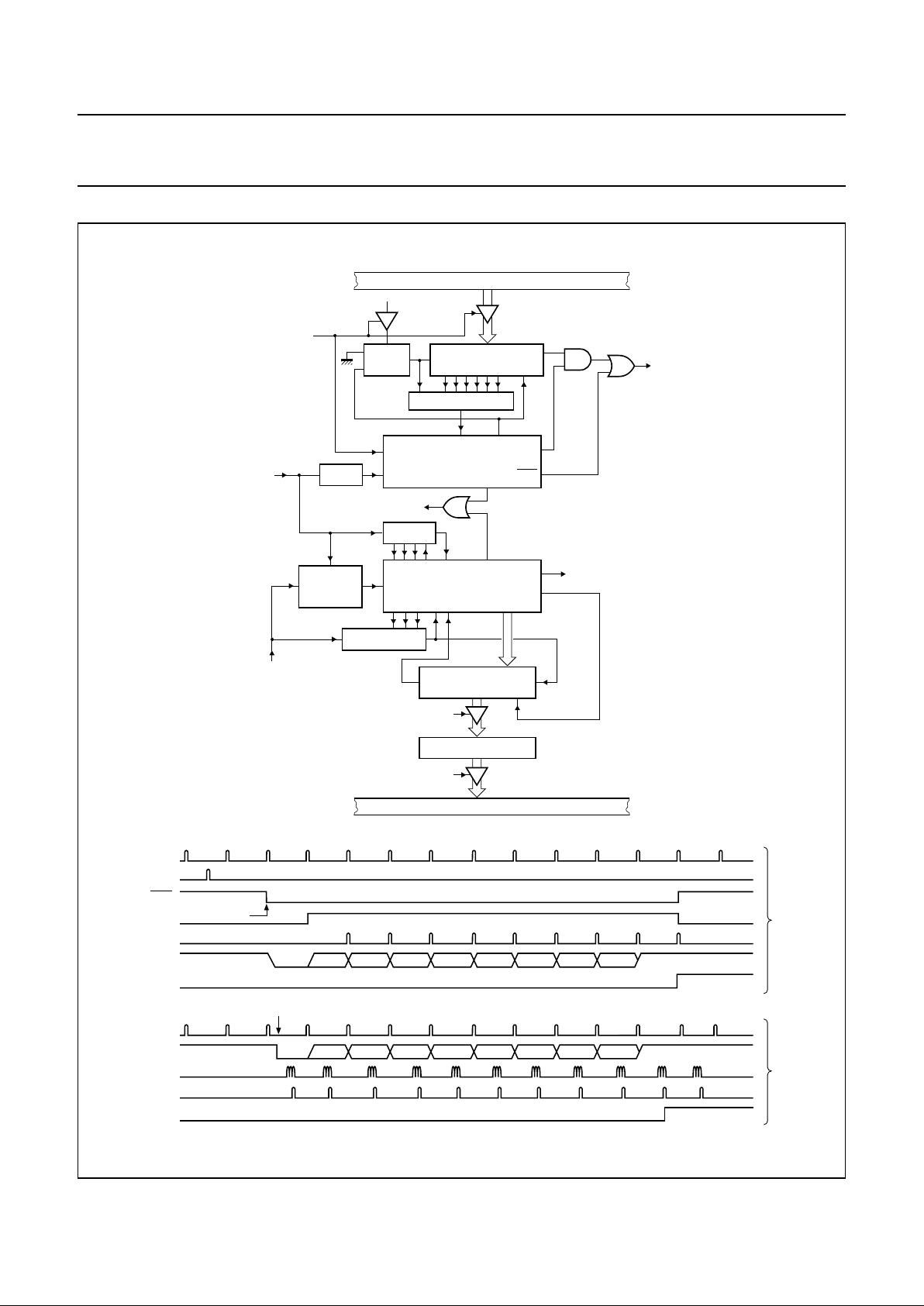
1999 Aug 19 70
Philips Semiconductors Objective Specification
Single-chip 8-bit microcontroller with CAN controller P8xC591
Fig.26 Serial Port Mode 1.
handbook, full pagewidth
TxD
SBUF
Shift
TX CONTROL
T1
Start
TX Clock
Data
Send
S
TB8
write to SBUF
serial port interrupt
BAUD RATE CLOCK
sample
Q
D
CL
ZERO DETECTOR
1-to-0
TRANSITION
DETECTOR
RxD
BIT DETECTOR
INPUT SHIFT REGISTER
(9 BITS)
SBUF
load SBUF
read SBUF
R1
RX CONTROL
1FFH
shift
RX Clock
Start
load
SBUF
Shift
MHI027
D4 D5 D6D3D2D1D0
Start
bit
÷16 Reset
D7
Stop bit
D4 D5 D6D3D2D1D0
Start
bit
D7
Stop bit
Transmit
Receive
TX Clock
write to SBUF
Send
Data
Shift
TxD
TI
RX Clock
RxD
Bit detector sample times
Shift
RI
S1P1
80C51 INTERNAL BUS
80C51 INTERNAL BUS
÷16
÷16
Page 71

1999 Aug 19 71
Philips Semiconductors Objective Specification
Single-chip 8-bit microcontroller with CAN controller P8xC591
Fig.27 Serial Port Mode 2 and 3.
handbook, full pagewidth
TxD
SBUF
Shift
TX CONTROL
T1
Stop bit
gen.
Start
TX Clock
Data
Send
S
TB8
write to SBUF
serial port interrupt
BAUD RATE CLOCK
sample
Q
D
CL
ZERO DETECTOR
1-to-0
TRANSITION
DETECTOR
RxD
BIT DETECTOR
INPUT SHIFT REGISTER
(9 BITS)
SBUF
load SBUF
read SBUF
R1
RX CONTROL
1FFH
shift
RX Clock
Start
load
SBUF
Shift
MHI028
D4 D5 D6D3D2D1D0
Start
bit
D7 TB8
Stop bit
D4 D5 D6D3D2D1D0
Start
bit
D7 TB8
Stop bit
Transmit
Receive
TX Clock
write to SBUF
Send
Data
Shift
TxD
TI
Stop bit gen.
RX Clock
RxD
Bit detector sample times
Shift
RI
S1P1
80C51 INTERNAL BUS
80C51 INTERNAL BUS
÷16 Reset
÷16
÷16
Page 72

1999 Aug 19 72
Philips Semiconductors Objective Specification
Single-chip 8-bit microcontroller with CAN controller P8xC591
14.5 Enhanced UART
The UART operates in all of the usual modes that are
described in the Section of Standard Serial Interface,
80C51-Based 8-Bit Microcontrollers. In addition the UART
can perform framing error detect by looking for missing
stop bits, and automatic address recognition. The UART
also fully supports multiprocessor communication as does
the standard 80C51 UART.
When used for framing error detect the UART looks for
missing stop bits in the communication. A missing bit will
set the FE bit in the S0CON register. The FE bit shares the
S0CON.7 bit with SM0 and the function of S0CON.7 is
determined by PCON.6 (SMOD0) see Table 50. If SMOD0
is set then S0CON.7 functions as FE. S0CON.7 functions
as SM0 when SMOD0 is cleared. When as FE S0CON.7
can only be cleared by software. Refer to Figure 25.
14.5.1 AUTOMATIC ADDRESS RECOGNITION
Automatic Address Recognition is a feature which allows
the UART to recognize certain addresses in the serial bit
stream by using hardware to make the comparisons. This
feature saves a great deal of software overhead by
eliminating the need for the software to examine every
serial address which passes by the serial port. This feature
is enabled by setting the SM2 bit in S0CON. In the 9 bit
UART modes, mode 2 and mode 3, the Receive Interrupt
flag (RI) will be automatically set when the received byte
contains either the “Given” address or the “Broadcast”
address. The 9 bit mode requires that the 9th information
bit is a 1 to indicate that the received information is an
address and not data. Automatic address recognition is
shown in Figure 29.
The 8 bit mode is called Mode 1. In this mode the RI flag
will be set if SM2 is enabled and the information received
has a valid stop bit following the 8 address bits and the
information is either a Given or Broadcast address.
14.5.2 S
ERIAL PORT CONTROL REGISTER (S0CON)
Table 49 Serial Port Control Register (address 98H)
Table 50 Description of S0CON bits
76543210
SM0/FE SM1 SM2 REN TB8 RB8 TI RI
BIT SYMBOL DESCRIPTION
7FE
SM0
Framing Error bit. This bit is set by the receiver when an invalid stop bit is detected. The FE
bit is not cleared by valid frames but should be cleared by software.
Serial Port Mode Bit 0, (SMOD0 must = 0 to access bit SM0), see Table 46.
6 SM1 These bits are used to select the serial port mode; see Table 46.
5 SM2 Enables the Automatic Address Recognition feature in Modes 2 and 3. If SM2 = 1, then RI
will not be set unless the received 9th data bit (RB8) is a logic 1, indicating an address, and the
received byte is a Given or Broadcast Address. In Mode 1, if SM2 = 1, then RI will not be
activated unless a valid stop bit was not received, and the received byte is a Given or
Broadcast Address. In Mode 0, SM2 should be a logic 0.
4 REN Enables serial reception. Set by software to enable reception. Clear by software to disable
reception.
3 TB8 The 9th data bit that will be transmitted in Modes 2 and 3. Set or clear by software as desired.
2 RB8 In modes 2 and 3, the 9th data bit that was received. In Mode 1, if SM2 = 0, RB8 is the stop bit
that was received. In Mode 0, RB8 is not used.
1TITransmit Interrupt flag. Set by hardware at the end of the 8th bit time in Mode 0, or at the
beginning of the stop bit in the other modes, in any serial transmission. Must be cleared by
software.
0RIReceive Interrupt flag. Set by hardware at the end of the 8th bit time in Mode 0, or halfway
through the stop bit time in the other modes, in any serial reception (except see SM2). Must
be cleared by software.
Page 73
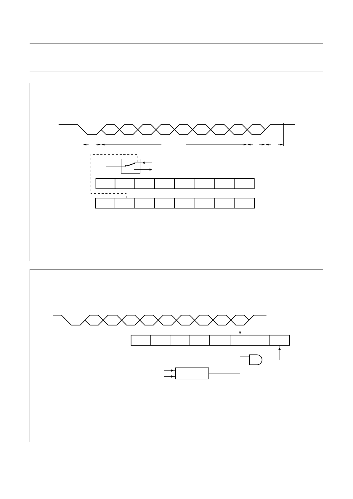
1999 Aug 19 73
Philips Semiconductors Objective Specification
Single-chip 8-bit microcontroller with CAN controller P8xC591
Fig.28 UART Framing Error Detection.
handbook, full pagewidth
MHI029
SM0/FE SM1 SM2 REN TB8 RB8 TI RI
SMOD1 SMOD0
0 : S0CON.7 = SM0
1 : S0CON.7 = FE
POF WLE GF1 GF0 PD IDL
SCON
(98H)
PCON
(87H)
Set FE BIT if STOP BIT is 0 (FRAMING ERROR)
SM0 to UART MODE CONTROL
D0 D1 D2 D3 D4 D5 D6 D7 D8
START
bit
DATA byte
only
in
MODE 2, 3
STOP
bit
Fig.29 UART Multiprocessor Communication, Automatic Address Recognition.
handbook, full pagewidth
MHI030
SM0 SM1 SM2 REN TB8
11 11X
10
COMPARATOR
RB8 TI RI
SCON
(98H)
D0 D1 D2 D3 D4 D5 D6 D7 D8
RECEIVED ADDRESS D0 TO D7
PROGRAMMED ADDRESS
In UART Mode 2 or Mode 3 and SM2 = 1:
Interrupt if REN = 1, RB8 = 1 and “Received Address” = “Programmed Address”
± when own address received, clear SM2 to receive data bytes
± when all data bytes have been received: set SM2 to wait for next address.
Page 74

1999 Aug 19 74
Philips Semiconductors Objective Specification
Single-chip 8-bit microcontroller with CAN controller P8xC591
Mode 0 is the Shift Register mode and SM2 is ignored.
Using the Automatic Address Recognition feature allows a
master to selectively communicate with one or more
slaves by invoking the Given slave address or addresses.
All of the slaves may be contacted by using the Broadcast
address. All of the slaves may be contacted by using the
Broadcast address. Two Special Function Registers are
used to define the slave’s address, SADDR, and the
address mask, SADEN. SADEN is used to define which
bits in the SADDR are to be used and which bits are “don’t
care”. The SADEN mask can be logically ANDed with the
SADDR to create the “Given” address which the master
will use for addressing each of the slaves. Use of the Given
address allows multiple slaves to be recognized while
excluding others. The following examples will help to show
the versatility of this scheme:
Slave 0 SADDR = 1100 0000
SADEN = 1111 1101
Given = 1100 00X0
Slave 1 SADDR = 1100 0000
SADEN = 1111 1110
Given = 1100 000X
In the above example SADDR is the same and the SADEN
data is used to differentiate between the two salves. Slave
0 requires as 0 in bit 0 and it ignores bit 1. Slave 1 requires
a 0 in bit 1 and bit 0 is ignored. A unique address for Slave
0 would be 1100 0010 since slave 1 requires a 0 in bit 1. A
unique address for Slave 1 would be 1100 0001 since a 1
in bit 0 will exclude slave 0. Both slaves can be selected at
the same time by an address which has bit 0 = 0 (for Slave
0) and bit 1 = 0 (for Slave 1). Thus, both could be
addressed with 1100 0000.
In a more complex system the following could be used to
select Slaves 1 and 2 while excluding Slave 0:
Slave 0 SADDR = 1100 0000
SADEN = 1111 1001
Given = 1100 0XX0
Slave 1 SADDR = 1110 0000
SADEN = 1111 1010
Given = 1110 0X0X
Slave 2 SADDR = 1110 0000
SADEN = 1111 1100
Given = 1110 00XX
In the above example the differentiation among the 3
Slaves is in the lower 3 address bits. Slave 0 requires that
bit 0 = 0 and it can be uniquely addressed by 1110 0110.
Slave 1 requires that bit 1 = 0 and it can be uniquely
addressed by 1110 and 0101. Slave 2 requires that bit 2 =
0 and its unique address is 1110 0011. To select Slaves 0
and 1 and exclude Slave 2 use address 1110 0100, since
it is necessary to make bit 2 = 1 to exclude Slave 2.
The Broadcast Address for each slave is created by taking
the logical OR of SADDR and SADEN. Zeros in this result
are trended as don’t cares. In most cases, interpreting the
don’t-cares as ones, the broadcast address will be FF
hexadecimal.
Upon reset SADDR (SFR address 0A9H) and SADEN
(SFR address 0B9H) are leaded with 0s. This produces a
given address of all “don’t cares” as well as a Broadcast
address of all “don’t cares”. This effectively disables the
Automatic Addressing mode and allows the
microcontroller to use standard 80C51 type UART drivers
which do not make use of this feature.
15 SIO1, I
2
C SERIAL IO
The I2C bus uses two wires (SDA and SCL) to transfer
information between devices connected to the bus. The
main features of the bus are:
• Bidirectional data transfer between masters and slaves
• Multimaster bus (no central master)
• Arbitration between simultaneously transmitting
masters without corruption of serial data on the bus
• Serial clock synchronization allows devices with
different bit rates to communicate via one serial bus
• Serial clock synchronization can be used as a
handshake mechanism to suspend and resume serial
transfer
• The I2C bus may be used for test and diagnostic
purposes
The I/O pins P1.6 and P1.7 must be set to Open Drain
(SCL and SDA).
The 8xC591 on-chip I2C logic provides a serial interface
that meets the I2C bus specification. The SIO1 logic
handles bytes transfer autonomously. It also keeps track
of serial transfers, and a status register (S1STA) reflects
the status of SIO1 and the I2C bus.
Page 75

1999 Aug 19 75
Philips Semiconductors Objective Specification
Single-chip 8-bit microcontroller with CAN controller P8xC591
The CPU interfaces to the I2C logic via the following four
special function registers: S1CON (SIO1 control register),
S1STA (SIO1 status register), S1DAT (SIO1 data
register), and S1ADR (SIO1 slave address register). The
SIO1 logic interfaces to the external I2C bus via two port 1
pins: P1.6/SCL (serial clock line) and P1.7/SDA (serial
data line).
A typical I2C bus configuration is shown in Figure 30, and
Figure 31 shows how a data transfer is accomplished on
the bus. Depending on the state of the direction bit (R/W),
two types of data transfers are possible on the I2C bus:
1. Data transfer from a master transmitter to a slave
receiver. The first byte transmitted by the master is the
slave address. Next follows a number of data bytes.
The slave returns an acknowledge bit after each
received byte.
2. Data transfer from a slave transmitter to a master
receiver. The first byte (the slave address) is
transmitted by the master. The slave then returns an
acknowledge bit. Next follows the data bytes
transmitted by the slave to the master. The master
returns an acknowledge bit after all received bytes
other than the last byte. At the end of the last received
byte, a not acknowledge is returned.
The master device generates all of the serial clock pulses
and the START and STOP conditions. A transfer is ended
with a STOP condition or with a repeated START
condition. Since a repeated START condition is also the
beginning of the next serial transfer, the I2C bus will not be
released.
15.1 Modes of Operation
The on-chip SIO1 logic may operate in the following four
modes:
1. Master Transmitter Mode:
Serial data output through P1.7/SDA while P1.6/SCL
outputs the serial clock. The first byte transmitted
contains the slave address of the receiving device (7
bits) and the data direction bit. In this case the data
direction bit (R/W) will be logic 0, and we say that a “W”
is transmitted. Thus the first byte transmitted is
SLA+W. Serial data is transmitted 8 bits at a time. After
each byte is transmitted, an acknowledge bit is
received. START and STOP conditions are output to
indicate the beginning and the end of a serial transfer.
2. Master Receiver Mode:
The first byte transmitted contains the slave address of
the transmitting device (7 bits) and the data direction
bit. In this case the data direction bit (R/W) will be logic
1, and we say that an “R” is transmitted. Thus the first
byte transmitted is SLA+R. Serial data is received via
P1.7/SDA while P1.6/SCL outputs the serial clock.
Serial data is received 8 bits at a time. After each byte
is received, an acknowledge bit is transmitted. START
and STOP conditions are output to indicate the
beginning and end of a serial transfer.
3. Slave Receiver Mode:
Serial data and the serial clock are received through
P1.7/SDA and P1.6/SCL. After each byte is received,
an acknowledge bit is transmitted. START and STOP
conditions are recognized as the beginning and end of
a serial transfer. Address recognition is performed by
hardware after reception of the slave address and
direction bit.
4. Slave Transmitter Mode:
The first byte is received and handled as in the slave
receiver mode. However, in this mode, the direction bit
will indicate that the transfer direction is reversed.
Serial data is transmitted via P1.7/SDA while the serial
clock is input through P1.6/SCL. START and STOP
conditions are recognized as the beginning and end of
a serial transfer.
In a given application, SIO1 may operate as a master and
as a slave. In the slave mode, the SIO1 hardware looks for
its own slave address and the general call address. If one
of these addresses is detected, an interrupt is requested.
When the microcontroller wishes to become the bus
master, the hardware waits until the bus is free before the
master mode is entered so that a possible slave action is
not interrupted. If bus arbitration is lost in the master mode,
SIO1 switches to the slave mode immediately and can
detect its own slave address in the same serial transfer.
Page 76
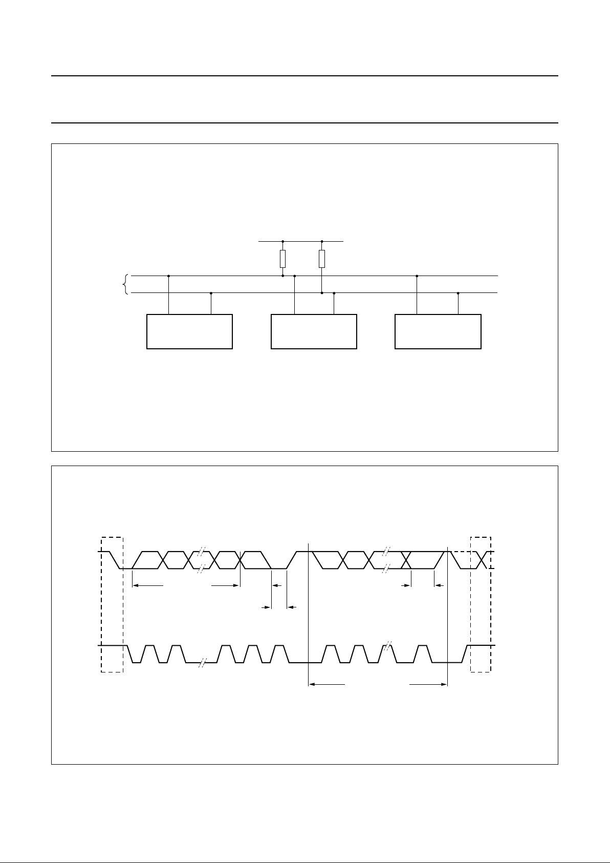
1999 Aug 19 76
Philips Semiconductors Objective Specification
Single-chip 8-bit microcontroller with CAN controller P8xC591
Fig.30 Typical I2C Bus configuration.
handbook, full pagewidth
MHI031
OTHER DEVICE WITH
I
2
C INTERFACE
R
P
OTHER DEVICE WITH
I
2
C INTERFACE
R
P
SDA
V
DD
SCL
P1.7/SDA P1.6/SCL
8xC591
I2C-bus
Fig.31 Data Transfer on the I2C Bus.
handbook, full pagewidth
MHI032
slave address
R/W
direction
bit
acknowledgment
signal from receiver
repeated if more bytes
are transferred
clock line held low while
interrupts are serviced
acknowledgment
signal from receiver
MSB
12 789
ACK
1 2 3-8 9
ACK
SDA
SCL
STOP
condition
START
condition
repeated
START
condition
P/SS
Page 77

1999 Aug 19 77
Philips Semiconductors Objective Specification
Single-chip 8-bit microcontroller with CAN controller P8xC591
15.2 SIO1 Implementation and Operation
Figure 32 shows how the on-chip I2C bus interface is
implemented, and the following text describes the
individual blocks.
15.2.1 INPUT FILTERS AND OUTPUT STAGES
The input filters have I2C compatible input levels. If the
input voltage is less than 1.5 V, the input logic level is
interpreted as 0; if the input voltage is greater than 3.0 V,
the input logic level is interpreted as 1. Input signals are
synchronized with the internal clock (f
CLK
/4), and spikes
shorter than three oscillator periods are filtered out.
The output stages consist of open drain transistors that
can sink 3 mA at V
OUT
< 0.4 V. These open drain outputs
do have clamping diodes to VDD. Thus, precautions have
to be considered, if a powered-down 8xC591 on one board
clamps the I2C bus externally.
15.2.2 ADDRESS REGISTER, S1ADR
This 8-bit special function register may be loaded with the
7-bit slave address (7 most significant bits) to which SIO1
will respond when programmed as a slave transmitter or
receiver. The LSB (GC) is used to enable general call
address (00H) recognition.
15.2.3 COMPARATOR
The comparator compares the received 7-bit slave
address with its own slave address (7 most significant bits
in S1ADR). It also compares the first received 8-bit byte
with the general call address (00H). If an equality is found,
the appropriate status bits are set and an interrupt is
requested.
15.2.4 SHIFT REGISTER, S1DAT
This 8-bit special function register contains a byte of serial
data to be transmitted or a byte which has just been
received. Data in S1DAT is always shifted from right to left;
the first bit to be transmitted is the MSB (bit 7) and, after a
byte has been received, the first bit of received data is
located at the MSB of S1DAT. While data is being shifted
out, data on the bus is simultaneously being shifted in;
S1DAT always contains the last byte present on the bus.
Thus, in the event of lost arbitration, the transition from
master transmitter to slave receiver is made with the
correct data in S1DAT.
Page 78
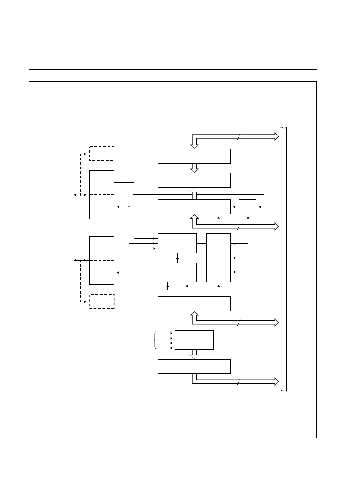
1999 Aug 19 78
Philips Semiconductors Objective Specification
Single-chip 8-bit microcontroller with CAN controller P8xC591
Fig.32 I2C Bus Interface Block Diagram.
handbook, full pagewidth
MHI033
8
8
8
8
ADDRESS REGISTER
COMPARATOR
SHIFT REGISTER
CONTROL REGISTER
ACK
TIMING
&
CONTROL
LOGIC
INPUT
FILTER
OUTPUT
STAGE
INPUT
FILTER
P1.7
OUTPUT
STAGE
1/4 f
OSC
INTERRUPT
TIMER 1
OVERFLOW
ARBITRATION &
SYNC LOGIC
STATUS
DECODER
SERIAL CLOCK
GENERATOR
S1ADR
S1DAT
STATUS REGISTER
S1STA
STATUS BITS
S1CON
P1.7/SDA
P1.6
P1.6/SCL
INTERNAL BUS
Page 79
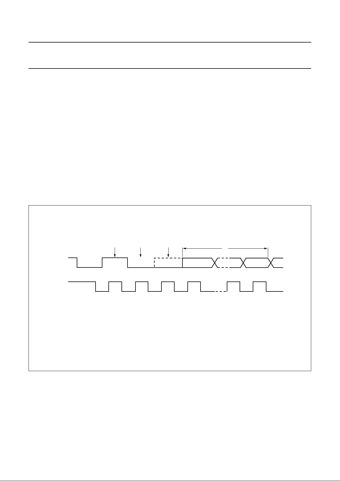
1999 Aug 19 79
Philips Semiconductors Objective Specification
Single-chip 8-bit microcontroller with CAN controller P8xC591
15.2.5 ARBITRATION AND SYNCHRONIZATION LOGIC
In the master transmitter mode, the arbitration logic checks
that every transmitted logic 1 actually appears as a logic 1
on the I2C bus. If another device on the bus overrules a
logic 1 and pulls the SDA line low, arbitration is lost, and
SIO1 immediately changes from master transmitter to
slave receiver. SIO1 will continue to output clock pulses
(on SCL) until transmission of the current serial byte is
complete.
Arbitration may also be lost in the master receiver mode.
Loss of arbitration in this mode can only occur while SIO1
is returning a not acknowledge: (logic 1) to the bus.
Arbitration is lost when another device on the bus pulls this
signal LOW. Since this can occur only at the end of a serial
byte, SIO1 generates no further clock pulses. Figure 33
shows the arbitration procedure.
The synchronization logic will synchronize the serial clock
generator with the clock pulses on the SCL line from
another device. If two or more master devices generate
clock pulses, the mark duration is determined by the
device that generates the shortest marks, and the space
duration is determined by the device that generates the
longest spaces. Figure 34 shows the synchronization
procedure.
A slave may stretch the space duration to slow down the
bus master. The space duration may also be stretched for
handshaking purposes. This can be done after each bit or
after a complete byte transfer. SIO1 will stretch the SCL
space duration after a byte has been transmitted or
received and the acknowledge bit has been transferred.
The serial interrupt flag (SI) is set, and the stretching
continues until the serial interrupt flag is cleared.
Fig.33 Arbitration Procedure.
handbook, full pagewidth
MHI034
SDA
SCL
1234 89
ACK
(2)(1) (1)
(3)
(1) Another device transmits identical serial data.
(2) Another device overrules a logic 1 (dotted line) transmitted by SIO1 (master) by pulling the SDA line low. Arbitration is lost,
and SIO1 enters the slave receiver mode.
(3) SIO1 is in the slave receiver mode but still generates clock pulses until the current byte has been transmitted. SIO1 will not
generate clock pulses for the next byte. Data on SDA originates from the new master once it has won arbitration.
Page 80

1999 Aug 19 80
Philips Semiconductors Objective Specification
Single-chip 8-bit microcontroller with CAN controller P8xC591
Fig.34 Serial Clock Synchronization.
handbook, full pagewidth
MHI035
SDA
SCL
(1) (3) (1)
(2)
mark
duration
space duration
(1) Another service pulls the SCL line low before the SIO “mask” duration is complete. The serial clock generator
is immediately reset and commences with the “space” duration by pulling SCL low.
(2) Another device still pulls the SCL line low after SIO1 releases SCL. The serial clock generator is forced into
the wait state until the SCL line is released.
(3) The SCL line is released, and the serial clock generator commences with the mark duration.
15.2.6 SERIAL CLOCK GENERATOR
This programmable clock pulse generator provides the
SCL clock pulses when SIO1 is in the master transmitter
or master receiver mode. It is switched off when SIO1 is in
a slave mode. The programmable output clock
frequencies are: f
CLK
/120, f
CLK
/9600, and the Timer 1
overflow rate divided by eight. The output clock pulses
have a 50% duty cycle unless the clock generator is
synchronized with other SCL clock sources as described
above.
15.2.7 TIMING AND CONTROL
The timing and control logic generates the timing and
control signals for serial byte handling. This logic block
provides the shift pulses for S1DAT, enables the
comparator, generates and detects start and stop
conditions, receives and transmits acknowledge bits,
controls the master and slave modes, contains interrupt
request logic, and monitors the I2C bus status.
15.2.8 CONTROL REGISTER, S1CON
This 7-bit special function register is used by the
microcontroller to control the following SIO1 functions:
start and restart of a serial transfer, termination of a serial
transfer, bit rate, address recognition, and
acknowledgment.
15.2.9 STATUS DECODER AND STATUS REGISTER
The status decoder takes all of the internal status bits and
compresses them into a 5-bit code. This code is unique for
each I2C bus status. The 5-bit code may be used to
generate vector addresses for fast processing of the
various service routines. Each service routine processes a
particular bus status. There are 26 possible bus states if all
four modes of SIO1 are used. The 5-bit status code is
latched into the five most significant bits of the status
register when the serial interrupt flag is set (by hardware)
and remains stable until the interrupt flag is cleared by
software. The three least significant bits of the status
register are always zero. If the status code is used as a
vector to service routines, then the routines are displaced
by eight address locations. Eight bytes of code is sufficient
for most of the service routines (see the software example
in this section).
15.2.10 THE FOUR SIO1 SPECIAL FUNCTION REGISTERS
The microcontroller interfaces to SIO1 via four special
function registers. These four SFRs (S1ADR, S1DAT,
S1CON, and S1STA) are described individually in the
following sections.
Page 81

1999 Aug 19 81
Philips Semiconductors Objective Specification
Single-chip 8-bit microcontroller with CAN controller P8xC591
15.2.10.1 The Address Register, S1ADR
The CPU can read from and write to this 8-bit, directly
addressable SFR. S1ADR is not affected by the SIO1
hardware. The contents of this register are irrelevant when
SIO1 is in a master mode. In the slave modes, the seven
most significant bits must be loaded with the
microcontrollers own slave address, and, if the least
significant bit is set, the general call address (00H) is
recognized; otherwise it is ignored.
The most significant bit corresponds to the first bit received
from the I2C bus after a start condition. A logic 1 in S1ADR
corresponds to a high level on the I2C bus, and a logic 0
corresponds to a low level on the bus.
Table 51 Address Register S1ADR (address DBH)
Table 52 Description of S1ADR (DBH) bits
76543210
XXXXXXXGC
BIT SYMBOL DESCRIPTION
7 to 1 X Own slave address.
0 GC 0 = general call address is not recognized.
1 = general call address is recognized.
15.2.11 THE DATA REGISTER, S1DAT
S1DAT contains a byte of serial data to be transmitted or
a byte which has just been received. The CPU can read
from and write to this 8-bit, directly addressable SFR while
it is not in the process of shifting a byte. This occurs when
SIO1 is in a defined state and the serial interrupt flag is set.
Data in S1DAT remains stable as long as SI is set. Data in
S1DAT is always shifted from right to left: the first bit to be
transmitted is the MSB (bit 7), and, after a byte has been
received, the first bit of received data is located at the MSB
of S1DAT. While data is being shifted out, data on the bus
is simultaneously being shifted in; S1DAT always contains
the last data byte present on the bus. Thus, in the event of
lost arbitration, the transition from master transmitter to
slave receiver is made with the correct data in S1DAT.
S1DAT and the ACK flag form a 9-bit shift register which
shifts in or shifts out an 8-bit byte, followed by an
acknowledge bit. The ACK flag is controlled by the SIO1
hardware and cannot be accessed by the CPU. Serial data
is shifted through the ACK flag into S1DAT on the rising
edges of serial clock pulses on the SCL line. When a byte
has been shifted into S1DAT, the serial data is available in
S1DAT, and the acknowledge bit is returned by the control
logic during the ninth clock pulse. Serial data is shifted out
from S1DAT via a buffer (BSD7) on the falling edges of
clock pulses on the SCL line.
When the CPU writes to S1DAT, BSD7 is loaded with the
content of S1DAT.7, which is the first bit to be transmitted
to the SDA line (see Figure 36). After nine serial clock
pulses, the eight bits in S1DAT will have been transmitted
to the SDA line, and the acknowledge bit will be present in
ACK. Note that the eight transmitted bits are shifted back
into S1DAT.
Table 53 Address Register S1DAT (address DAH)
Table 54 Description of S1DAT (DAH) bits
76543210
SD7 SD6 SD5 SD4 SD3 SD2 SD1 SD0
BIT SYMBOL DESCRIPTION
7 to 0 SD7 to SD0 Eight bits to be transmitted or just received. A logic 1 in S1DAT corresponds to a high
level on the I
2
C bus, and a logic 0 corresponds to a low level on the bus. Serial data
shifts through S1DAT from right to left. Figure 35 shows how data in S1DAT is serially
transferred to and from the SDA line.
Page 82

1999 Aug 19 82
Philips Semiconductors Objective Specification
Single-chip 8-bit microcontroller with CAN controller P8xC591
15.2.12 THE CONTROL REGISTER, S1CON
The CPU can read from and write to this 8-bit, directly addressable SFR. Two bits are affected by the SIO1 hardware:
the SI bit is set when a serial interrupt is requested, and the STO bit is cleared when a STOP condition is present on the
I2C bus. The STO bit is also cleared when ENS1 = 0.
Table 55 Address Register S1CON (address D8H)
Table 56 Description of S1CON (D8H) bits
76543210
CR2 ENS1 STA STO SI AA CR1 CR0
BIT SYMBOL DESCRIPTION
7 CR2 Clock rate bit 2, see Table 57.
6 ENS1 Enable serial I/O. ENS1 = 0: I2C I/O disabled and reset. ENS1 = 1: serial I/O enabled.
5STAST ART flag. When this bit is set in slave mode, the hardware checks the I2C-bus and generates
a START condition if the bus is free or after the bus becomes free. If the device operates in
master mode it will generate a repeated START condition.
4STOSTOP flag. If this bit is set in a master mode a STOP condition is generated. A STOP condition
detected on the I2C-bus clears this bit. This bit may also be set in slave mode in order to recover
from an error condition. In this case no STOP condition is generated to the I2C-bus, but the
hardware releases the SDA and SCL lines and switches to the not selected receiver mode. The
STOP flag is cleared by the hardware.
3SISerial Interrupt flag. This flag is set and an interrupt request is generated, after any of the
following events occur:
• A START condition is generated in master mode.
• The own slave address has been received during AA = 1.
• The general call address has been received while S1ADR.0 and AA = 1.
• A data byte has been received or transmitted in master mode (even if arbitration is lost).
• A data byte has been received or transmitted as selected slave.
• A STOP or START condition is received as selected slave receiver or transmitter.
While the SI flag is set, SCL remains LOW and the serial transfer is suspended. SI must be
reset by software.
2AAAssert Acknowledge flag. When this bit is set, an acknowledge is returned after any one of the
following conditions:
• Own slave address is received.
• General call address is received (S1ADR.0 = 1).
• A data byte is received, while the device is programmed to be a master receiver.
• A data byte is received. while the device is a selected slave receiver.
When the bit is reset, no acknowledge is returned. Consequently, no interrupt is requested when
the own address or general call address is received.
1 CR1 Clock rate bits 1 and 0; see Table 57.
0 CR0
Page 83

1999 Aug 19 83
Philips Semiconductors Objective Specification
Single-chip 8-bit microcontroller with CAN controller P8xC591
15.2.12.1 ENS1, the SIO1 enable bit
ENS1 = “0”: When ENS1 is “0”, the SDA and SCL input
signals are ignored, SIO1 is in the not addressed slave
state, and the STO bit in S1CON is forced to 0. No other
bits are affected.
ENS1 = “1”: When ENS1 is 1, I2C is enabled. Note, that
P1.6 and P1.7 have to set to Open Drain by writing the Port
mode registers P1M1.x and P1M2.x bits 6 and 7 with a 1
(see Section 6.2 “Pin description”).
ENS1 should not be used to temporarily release SIO1 from
the I2C bus since, when ENS1 is reset, the I2C bus status
is lost. The AA flag should be used instead (see
description of the AA flag in the following text).
In the following text, it is assumed that ENS1 = 1.
15.2.12.2 STA, the START flag
STA = “1”: When the STA bit is set to enter a master mode,
the SIO1 hardware checks the status of the I2C bus and
generates a START condition if the bus is free. If the bus
is not free, then SIO1 waits for a STOP condition (which
will free the bus) and generates a START condition after a
delay of a half clock period of the internal serial clock
generator.
If STA is set while SIO1 is already in a master mode and
one or more bytes are transmitted or received, SIO1
transmits a repeated START condition. STA may be set at
any time. STA may also be set when SIO1 is an addressed
slave.
STA = “0”: When the STA bit is reset, no START condition
or repeated START condition will be generated.
15.2.12.3 STO, the STOP Flag
STO = “1”: When the STO bit is set while SIO1 is in a
master mode, a STOP condition is transmitted to the I2C
bus. When the STOP condition is detected on the bus, the
SIO1 hardware clears the STO flag. In a slave mode, the
STO flag may be set to recover from an error condition. In
this case, no STOP condition is transmitted to the I2C bus.
However, the SIO1 hardware behaves as if a STOP
condition has been received and switches to the defined
not addressed slave receiver mode. The STO flag is
automatically cleared by hardware.
If the STA and STO bits are both set, the a STOP condition
is transmitted to the I2C bus if SIO1 is in a master mode (in
a slave mode, SIO1 generates an internal STOP condition
which is not transmitted). SIO1 then transmits a START
condition.
STO = “0”: When the STO bit is reset, no STOP condition
will be generated.
Page 84
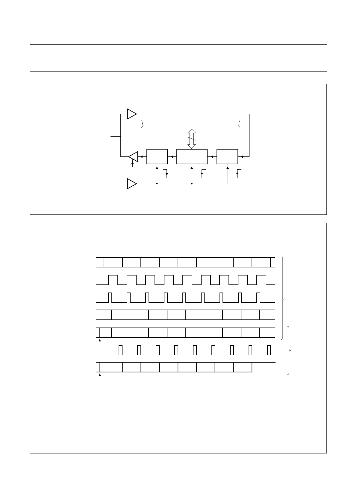
1999 Aug 19 84
Philips Semiconductors Objective Specification
Single-chip 8-bit microcontroller with CAN controller P8xC591
Fig.35 Serial Input/Output Configuration.
handbook, full pagewidth
MHI036
ACKBSD7
8
S1DAT
SHIFT PULSES
SDA
SCL
INTERNAL BUS
Fig.36 Shift-in and Shift-out Timing.
handbook, full pagewidth
MHI037
D7SDA
SCL
SHIFT ACK & S1DAT
SHIFT BSD7
loaded by the CPU
D6 D5 D4 D3 D2 D1 D0 A
(2) (2)(2)(2)(2)(2)(2)(2)
ACK A
(2)(1) (2)(2)(2)(2)(2)(2)(2)
S1DAT (1)
D6D7 D0 (3)D1D2D3D4D5BSD7
SHIFT
OUT
SHIFT
IN
(1) Valid data in S1DAT.
(2) Shifting data in S1DAT and ACK.
(3) High level on SDA.
Page 85

1999 Aug 19 85
Philips Semiconductors Objective Specification
Single-chip 8-bit microcontroller with CAN controller P8xC591
15.2.12.4 SI, the Serial Interrupt Flag
SI = “1”: When the SI flag is set, then, if the EA and ES1
(interrupt enable register) bits are also set, a serial
interrupt is requested. SI is set by hardware when one of
25 of the 26 possible SIO1 states is entered. The only state
that does not cause SI to be set is state F8H, which
indicates that no relevant state information is available.
While SI is set, the low period of the serial clock on the SCL
line is stretched, and the serial transfer is suspended. A
high level on the SCL line is unaffected by the serial
interrupt flag. SI must be reset by software.
SI = 0: When the SI flag is reset, no serial interrupt is
requested, and there is no stretching of the serial clock on
the SCL line.
15.2.12.5 AA, the Assert Acknowledge flag
AA = “1”: If the AA flag is set, an acknowledge (low level to
SDA) will be returned during the acknowledge clock pulse
on the SCL line when:
• The “own slave address” has been received
• The general call address has been received while the
general call bit (GC) in S1ADR is set
• A data byte has been received while SIO1 is in the
master receiver mode
• A data byte has been received while SIO1 is in the
addressed slave receiver mode
AA = “0”: if the AA flag is reset, a not acknowledge (high
level to SDA) will be returned during the acknowledge
clock pulse on SCL when:
• A data has been received while SIO1 is in the master
receiver mode
• A data byte has been received while SIO1 is in the
addressed slave receiver mode
When SIO1 is in the addressed slave transmitter mode,
state C8H will be entered after the last serial is transmitted
(see Figure 40). When SI is cleared, SIO1 leaves state
C8H, enters the not addressed slave receiver mode, and
the SDA line remains at a high level. In state C8H, the AA
flag can be set again for future address recognition.
When SIO1 is in the not addressed slave mode, its own
slave address and the general call address are ignored.
Consequently, no acknowledge is returned, and a serial
interrupt is not requested. Thus, SIO1 can be temporarily
released from the I2C bus while the bus status is
monitored. While SIO1 is released from the bus, START
and STOP conditions are detected, and serial data is
shifted in. Address recognition can be resumed at any time
by setting the AA flag. If the AA flag is set when the parts
own slave address or the general call address has been
partly received, the address will be recognized at the end
of the byte transmission.
15.2.12.6 CR0, CR1, and CR2, the Clock Rate Bits
These three bits determine the serial clock frequency
when SIO1 is in a master mode. The various serial rates
are shown in Table 57.
A 12.5 kHz bit rate may be used by devices that interface
to the I2C bus via standard I/O port lines which are
software driven and slow. 100kHz is usually the maximum
bit rate and can be derived from a 16 MHz, 12 MHz, or a
6 MHz oscillator. A variable bit rate (0.5 kHz to 62.5 kHz)
may also be used if Timer 1 is not required for any other
purpose while SIO1 is in a master mode.
The frequencies shown in Table 57 are unimportant when
SIO1 is in a slave mode. In the slave modes, SIO1 will
automatically synchronize with any clock frequency up to
100 kHz.
Page 86

1999 Aug 19 86
Philips Semiconductors Objective Specification
Single-chip 8-bit microcontroller with CAN controller P8xC591
15.2.13 THE STATUS REGISTER, S1STA
S1STA is an 8-bit read-only special function register. The
three least significant bits are always zero. The five most
significant bits contain the status code. There are 26
possible status codes. When S1STA contains F8H, no
relevant state information is available and no serial
interrupt is requested. All other S1STA values correspond
to defined SIO1 states. When each of these states is
entered, a serial interrupt is requested (SI = “1”). A valid
status code is present in S1STA one machine cycle after
SI is set by hardware and is still present one machine cycle
after SI has been reset by software.
Table 57 Serial clock rate
Note
1. These frequencies exceed the upper limit of 100 kHz of the I2C-bus specification and cannot be used in an I2C-bus
application.
CR2 CR1 CR0
BIT FREQUENCY (kHz) at f
CLK
f
CLK
DIVIDED BY
6 MHz 12 MHz 16 MHz
0 0 0 23 47 62.5 256
001275471 224
0 1 0 31 63 83.3 192
0 1 1 37 75 100 160
1 0 0 6.25 12.5 17 960
1 0 1 50 100 133
(1)
120
1 1 0 100 200 267
(1)
60
111
0.24 > 62.5
0 < 255
0.49 < 62.5
0 < 254
0.65 < 55.6
0 < 253
96 x (256 (reload value Timer 1))
Reload value Timer 1 in Mode 2.
15.2.14 MORE INFORMATION ON SIO1 OPERATING MODES
The four operating modes are:
• Master Transmitter
• Master Receiver
• Slave Receiver
• Slave Transmitter
Data transfers in each mode of operation are shown in
Figures 37 to 40. These figures contain the following
abbreviations:
Abbreviation Explanation
S Start condition
SLA 7-bit slave address
R Read bit (high level at SDA)
W Write bit (low level at SDA)
A Acknowledge bit (low level at SDA)
A Not acknowledge bit (high level at SDA)
Data 8-bit data byte
P Stop condition
In Figures 37 to 40, circles are used to indicate when the
serial interrupt flag is set. The numbers in the circles show
the status code held in the S1STA register. At these points,
a service routine must be executed to continue or
complete the serial transfer. These service routines are
not critical since the serial transfer is suspended until the
serial interrupt flag is cleared by software.
When a serial interrupt routine is entered, the status code
in S1STA is used to branch to the appropriate service
routine. For each status code, the required software action
and details of the following serial transfer are given in
Tables 61 to 65.
15.2.14.1 Master Transmitter Mode:
In the master transmitter mode, a number of data bytes are
transmitted to a slave receiver (see Figure 37). Before the
master transmitter mode can be entered, S1CON must be
initialized as in Table 58.
CR0, CR1, and CR2 define the serial bit rate. ENS1 must
be set to logic 1 to enable SIO1. If the AA bit is reset, SIO1
will not acknowledge its own slave address or the general
call address in the event of another device becoming
Page 87

1999 Aug 19 87
Philips Semiconductors Objective Specification
Single-chip 8-bit microcontroller with CAN controller P8xC591
master of the bus. In other words, if AA is reset, SIO0
cannot enter a slave mode. STA, STO, and SI must be
reset.
The master transmitter mode may now be entered by
setting the STA bit using the SETB instruction. The SIO1
logic will now test the I2C bus and generate a start
condition as soon as the bus becomes free. When a
START condition is transmitted, the serial interrupt flag
(SI) is set, and the status code in the status register
(S1STA) will be 08H. This status code must be used to
vector to an interrupt service routine that loads S1DAT with
the slave address and the data direction bit (SLA+W). The
SI bit in S1CON must then be reset before the serial
transfer can continue.
When the slave address and the direction bit have been
transmitted and an acknowledgment bit has been
received, the serial interrupt flag (SI) is set again, and a
number of status codes in S1STA are possible. There are
18H, 20H, or 38H for the master mode and also 68H, 78H,
or B0H if the slave mode was enabled (AA = logic 1). The
appropriate action to be taken for each of these status
codes is detailed in Table 61. After a repeated start
condition (state 10H). SIO1 may switch to the master
receiver mode by loading S1DAT with SLA+R).
Table 58 Address Register S1CON (address D8H)
76543210
CR2 ENS1 STA STO SI AA CR1 CR0
bit rate 1 0 0 0 X bit rate
15.2.14.2 Master Receiver Mode
In the master receiver mode, a number of data bytes are
received from a slave transmitter (see Figure 38). The
transfer is initialized as in the master transmitter mode.
When the start condition has been transmitted, the
interrupt service routine must load S1DAT with the 7-bit
slave address and the data direction bit (SLA+R). The SI
bit in S1CON must then be cleared before the serial
transfer can continue.
When the slave address and the data direction bit have
been transmitted and an acknowledgment bit has been
received, the serial interrupt flag (SI) is set again, and a
number of status codes in S1STA are possible. These are
40H, 48H, or 38H for the master mode and also 68H, 78H,
or B0H if the slave mode was enabled (AA = logic 1). The
appropriate action to be taken for each of these status
codes is detailed in Table 62. ENS1, CR1, and CR0 are
not affected by the serial transfer and are not referred to in
Table 62. After a repeated start condition (state 10H),
SIO1 may switch to the master transmitter mode by
loading S1DAT with SLA+W.
15.2.14.3 Slave Receiver Mode:
In the slave receiver mode, a number of data bytes are
received from a master transmitter (see Figure 39). To
initiate the slave receiver mode, S1ADR and S1CON must
be loaded as in Table 59.
The upper 7 bits are the address to which SIO1 will
respond when addressed by a master. If the LSB (GC) is
set, SIO1 will respond to the general call address (00H);
otherwise it ignores the general call address.
CR0, CR1, and CR2 do not affect SIO1 in the slave mode.
ENS1 must be set to logic 1 to enable SIO1. The AA bit
must be set to enable SIO1 to acknowledge its own slave
address or the general call address. STA, STO, and SI
must be reset.
When S1ADR and S1CON have been initialized, SIO1
waits until it is addressed by its own slave address
followed by the data direction bit which must be “0” (W) for
SIO1 to operate in the slave receiver mode. After its own
slave address and the W bit have been received, the serial
interrupt flag (I) is set and a valid status code can be read
from S1STA. This status code is used to vector to an
interrupt service routine, and the appropriate action to be
taken for each of these status codes is detailed in
Table 63. The slave receiver mode may also be entered if
arbitration is lost while SIO1 is in the master mode (see
status 68H and 78H).
If the AA bit is reset during a transfer, SIO1 will return a not
acknowledge (logic 1) to SDA after the next received data
byte. While AA is reset, SIO1 does not respond to its own
slave address or a general call address. However, the I2C
bus is still monitored and address recognition may be
resumed at any time by setting AA. This means that the AA
bit may be used to temporarily isolate SIO1 from the I2C
bus.
Page 88
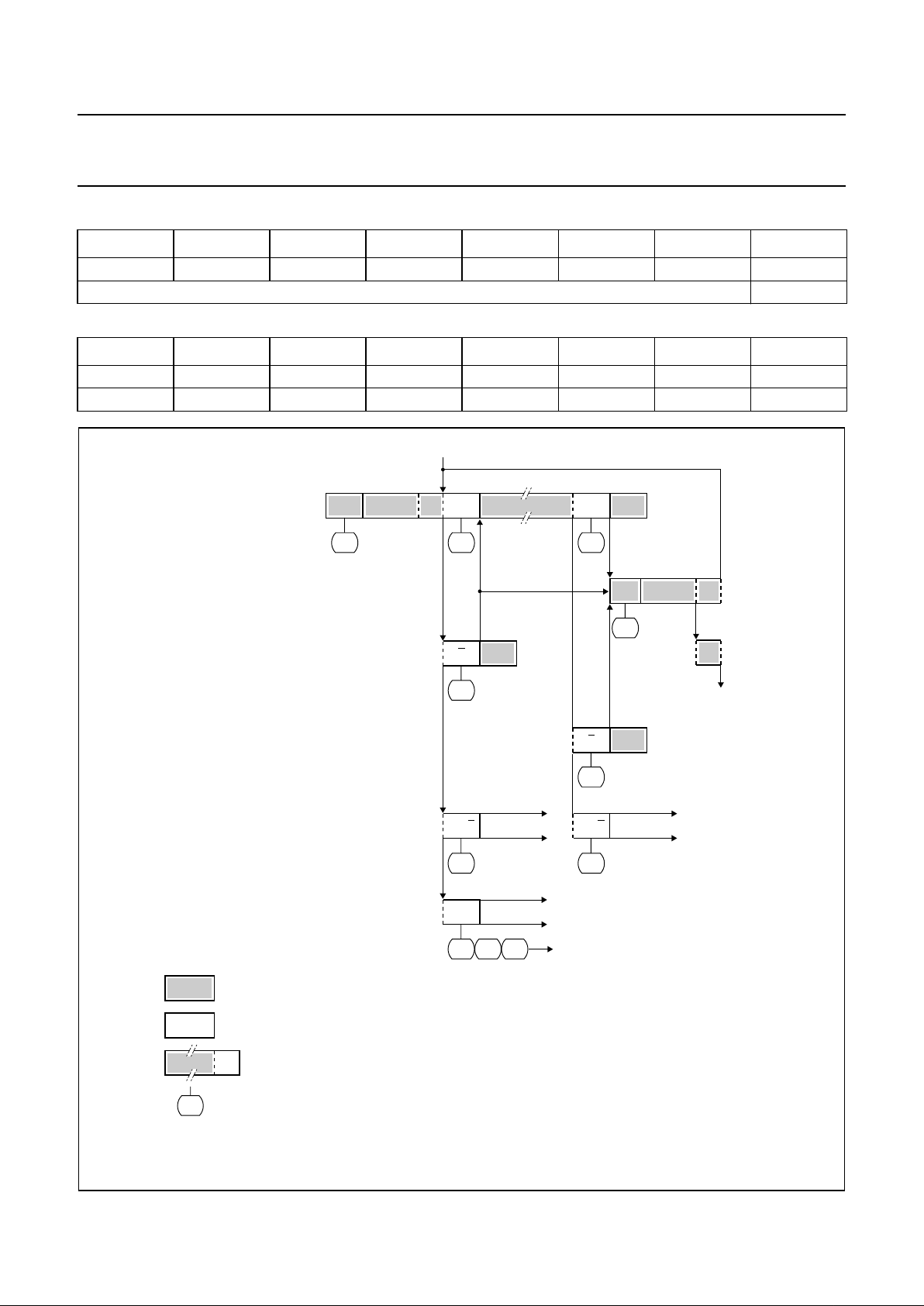
1999 Aug 19 88
Philips Semiconductors Objective Specification
Single-chip 8-bit microcontroller with CAN controller P8xC591
Table 59 Address Register S1ADR (DBH) (address 00H)
Table 60 Address Register S1CON (D8H) (address 00H)
76543210
XXXXXXXGC
own slave address
76543210
CR2 ENS1 STA STO SI AA CR1 CR0
X10001XX
Fig.37 Format and States in the Master Transmitter Mode.
handbook, full pagewidth
MHI038
n
THIS NUMBER (CONTAINED IN S1STA) CORRESPONDS TO A DEFINED STATE OF THE I
2
C-BUS
A
ANY NUMBER OF DATA BYTES AND THEIR ASSOCIATED ACKNOWLEDGE BITS
FROM SLAVE TO MASTER
FROM MASTER TO SLAVE
SUCCESSFUL TRANSMISSION
TO A SLAVE RECEIVER
NEXT TRANSFER STARTED WITH
A REPEATED START CONDITION
NOT ACKNOWLEDGE RECEIVED
AFTER THE SLAVE ADDRESS
NOT ACKNOWLEDGE RECEIVED
AFTER A DATA BYTE
ARBITRATION LOST IN SLAVE ADDRESS
OR DATA BYTE
ARBITRATION LOST AND ADDRESSED AS SLAVE
SLA
S PWA
MT
18H
PA
20H
OTHER MST
CONTINUES
38H
08H
SLAS W
R
10H
TO MST/REC MODE
ENTRY = MR
DATA
DATA
A
28H
OTHER MST
CONTINUES
38H
AorA AorA
A
OTHER MST
CONTINUES
TO CORRESPONDING
STATES IN SLAVE MODE
68H
78H 80H
PA
30H
(SEE TABLE 61)
Page 89

1999 Aug 19 89
Philips Semiconductors Objective Specification
Single-chip 8-bit microcontroller with CAN controller P8xC591
Fig.38 Format and States in the Master Receiver Mode.
handbook, full pagewidth
MHI039
n
THIS NUMBER (CONTAINED IN S1STA) CORRESPONDS TO A DEFINED STATE OF THE I
2
C-BUS
A
ANY NUMBER OF DATA BYTES AND THEIR ASSOCIATED ACKNOWLEDGE BITS
FROM SLAVE TO MASTER
FROM MASTER TO SLAVE
SUCCESSFUL RECEPTION
FROM A SLAVE TRANSMITTER
NEXT TRANSFER STARTED WITH
A REPEATED START CONDITION
NOT ACKNOWLEDGE RECEIVED
AFTER THE SLAVE ADDRESS
ARBITRATION LOST IN SLAVE ADDRESS
OR ACKNOWLEDGE BIT
ARBITRATION LOST AND ADDRESSED AS SLAVE
SLA
S PRA
MR
40H
PA
48H
A
OTHER MST
CONTINUES
38H
A
50H
08H
SLAS R
W
10H
TO MST/TRX MODE
ENTRY = MT
DATA
DATA
A
58H
DATA
AorA
OTHER MST
CONTINUES
38H
A
OTHER MST
CONTINUES
TO CORRESPONDING
STATES IN SLAVE MODE
68H
78H 80H
(SEE TABLE 62)
Page 90
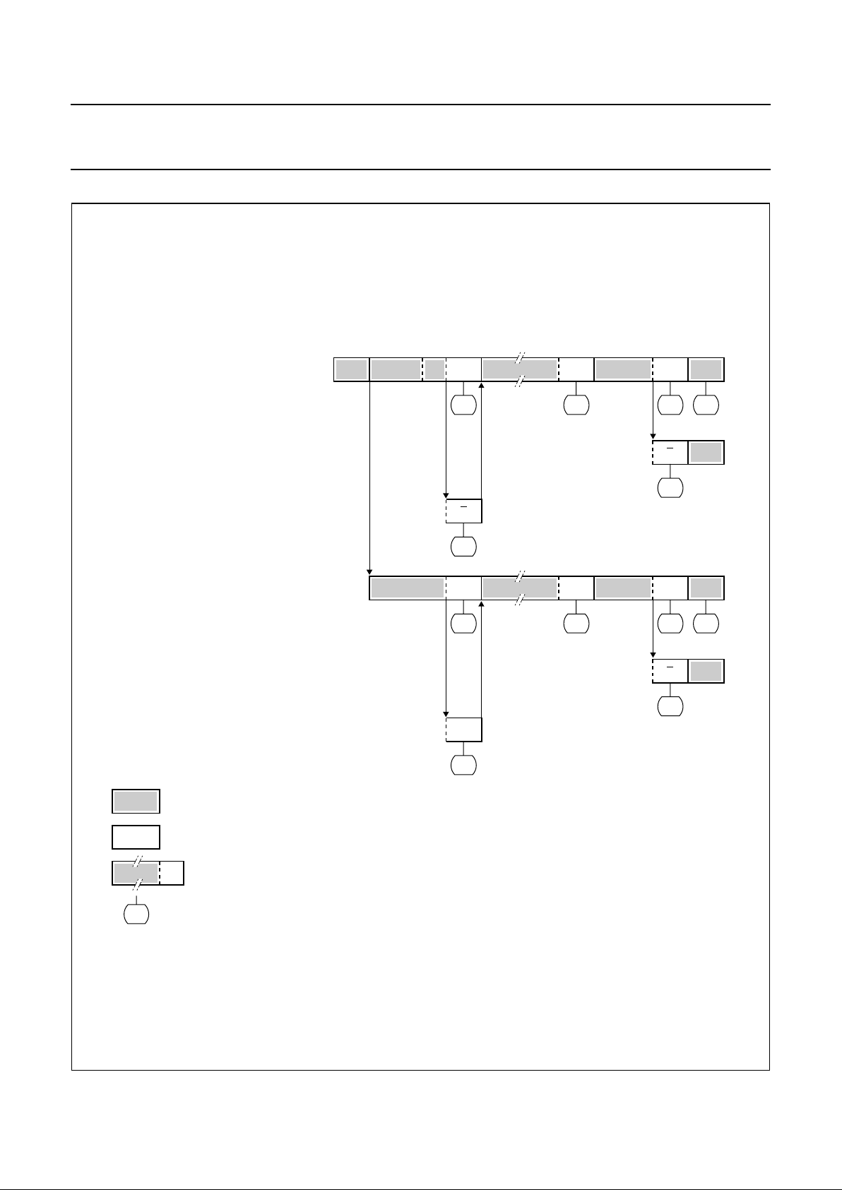
1999 Aug 19 90
Philips Semiconductors Objective Specification
Single-chip 8-bit microcontroller with CAN controller P8xC591
Fig.39 Format and States in the Slave Receiver Mode.
handbook, full pagewidth
MHI040
n
THIS NUMBER (CONTAINED IN S1STA) CORRESPONDS TO A DEFINED STATE OF THE I
2
C-BUS
A
ANY NUMBER OF DATA BYTES AND THEIR ASSOCIATED ACKNOWLEDGE BITS
FROM SLAVE TO MASTER
FROM MASTER TO SLAVE
RECEPTION OF THE OWN SLAVE ADDRESS
AND ONE OR MORE DATA BYTES
ALL ARE ACKNOWLEDGED
LAST DATA BYTE RECEIVED
IS NOT ACKNOWLEDGED
ARBITRATION LOST AS MST AND
ADDRESSED AS SLAVE
RECEPTION OF THE GENERAL CALL ADDRESS
AND ONE OR MORE DATA BYTES
LAST DATA BYTE IS NOT ACKNOWLEDGED
ARBITRATION LOST AS MST AND ADDRESSED
AS SLAVE BY GENERAL CALL
SLA
S WA
60H
A
68H
DATA
DATA
A
80H
A
P or SDATA A
80H
A0H
P or S
88H
GENERAL
CALL
A
70H
A
78H
DATA A
90H
A
P or SDATA
90H A0H
P or S
98H
A
(SEE TABLE 63)
Page 91
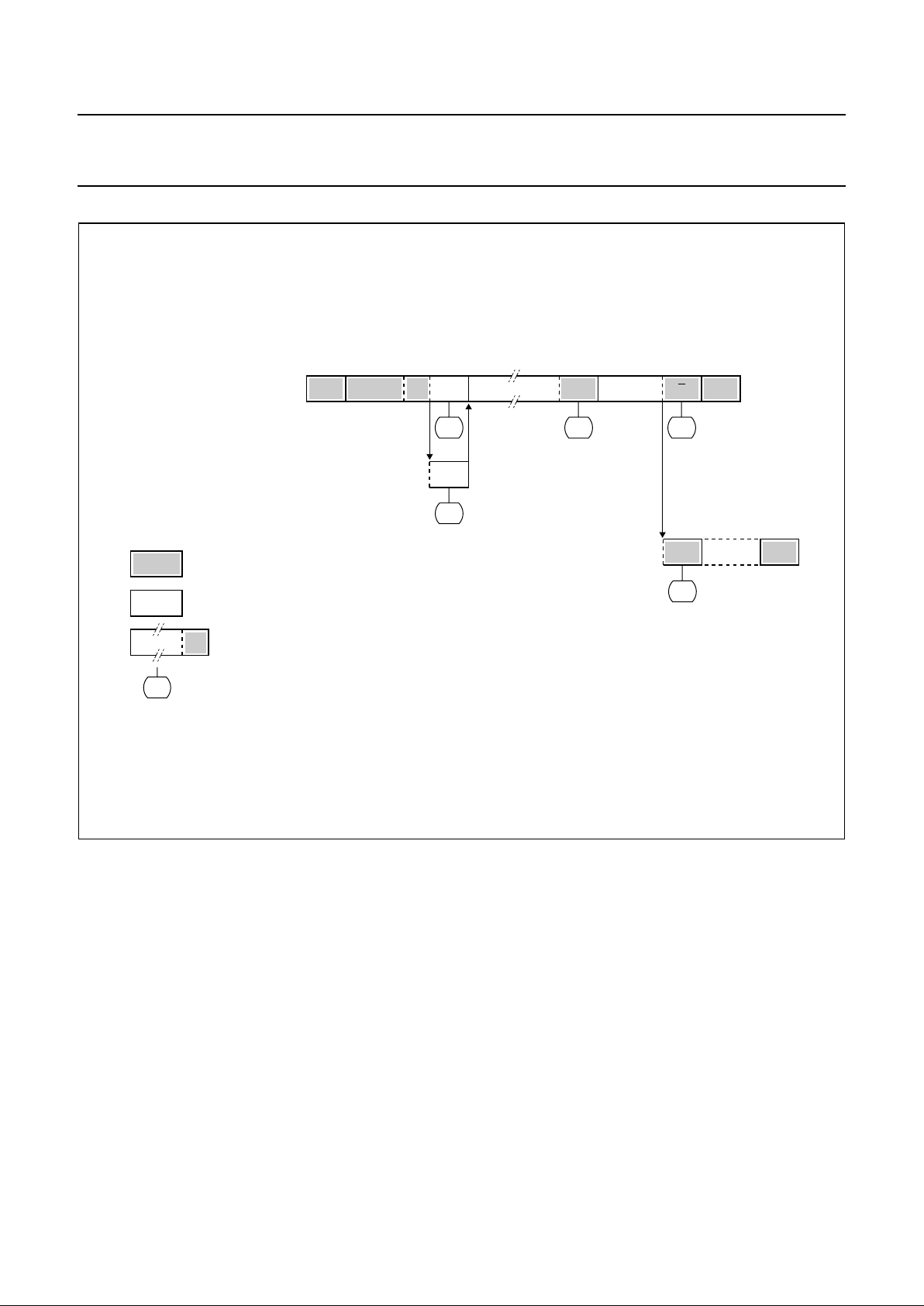
1999 Aug 19 91
Philips Semiconductors Objective Specification
Single-chip 8-bit microcontroller with CAN controller P8xC591
Fig.40 Format and States of the Slave Transmitter Mode.
handbook, full pagewidth
RECEPTION OF THE OWN
SLAVE ADDRESS AND
TRANSMISSION OF ONE
OR MORE DATA BYTES
ARBITRATION LOST AS MST
AND ADDRESSED AS SLAVE
LAST DATA BYTE TRANSMITTED.
SWITCHED TO NOT ADDRESSED
SLAVE (AA BIT IN S1CON = "0")
P or S
A
B0H
A All "1"s
C8H
MHI041
n
THIS NUMBER (CONTAINED IN S1STA) CORRESPONDS TO A DEFINED STATE OF THE I
2
C-BUS. SEE TABLE 9.
A
ANY NUMBER OF DATA BYTES AND THEIR ASSOCIATED ACKNOWLEDGE BITS
FROM SLAVE TO MASTER
FROM MASTER TO SLAVE
DATA
SLAS P or SRA
A8H
A
B8H
DATA A
C0H
DATA
(SEE TABLE 64)
Page 92

1999 Aug 19 92
Philips Semiconductors Objective Specification
Single-chip 8-bit microcontroller with CAN controller P8xC591
Table 61 Master Transmitter Mode
STATUS
CODE
(S1STA)
STATUS OF THE
I
2
C BUS AND
SIO1 HARDWARE
APPLICATION SOFTWARE RESPONSE
NEXT ACTION TAKEN BY SIO1
HARDWARE
TO/FROM S1DAT
TO S1CON
STA STO SI AA
08H A START condition has
been transmitted
Load SLA+W X 0 0 X SLA+W will be transmitted;
ACK bit will received
10H A repeated START
condition has been
transmitted
Load SLA+W or X 0 0 X As above
Load SLA+R X 0 0 X SLA+W will be transmitted; SIO1 will be
switched to MST/REC mode
18H SLA+W has been
transmitted; ACK has
been received
Load data byte or 0 0 0 X Data byte will be transmitted; ACK bit will
be received been received
no S1DAT action or 1 0 0 X Repeated START will be transmitted;
no S1DAT action or 0 1 0 X STOP condition will be transmitted;
STO flag will be reset
no S1DAT action 1 1 0 X STOP condition followed by a START
condition will be transmitted; STO flag will
be reset
20H SLA+W has been
transmitted; NOT ACK
has been received
Load data byte or 0 0 0 X Data byte will be transmitted; ACK will be
received
no S1DAT action or 1 0 0 X Repeated START will be transmitted;
no S1DAT action or 0 1 0 X STOP condition will be transmitted; STO
flag will be reset
no S1DAT action 1 1 0 X STOP condition followed by a START
condition will be transmitted; STO flag will
be reset
28H Data byte in S1DAT has
been transmitted; ACK
has been received
Load data byte or 0 0 0 X Data byte will be transmitted; ACK bit will
be received
no S1DAT action or 1 0 0 X Repeated START will be transmitted;
no S1DAT action or 0 1 0 X STOP condition will be transmitted; STO
flag will be reset
no S1DAT action 1 1 0 X STOP condition followed by a START
condition will be transmitted; STO flag will
be reset
30H Data byte in S1DAT has
been transmitted; NOT
ACK has been received
Load data byte or 0 0 0 X Data byte will be transmitted; ACK bit will
be received
no S1DAT action or 1 0 0 X Repeated START will be transmitted;
no S1DAT action or 0 1 0 X STOP condition will be transmitted; STO
flag will be reset
no S1DAT action 1 1 0 X STOP condition followed by a START
condition will be transmitted; STO flag will
be reset
38H Arbitration lost in
SLA+R/
W or Data bytes
No S1DAT action or 0 0 0 X I
2
C bus will be released; not addressed
slave will be entered
No S1DAT action 1 0 0 X A START condition will be transmitted
when the bus becomes free
Page 93

1999 Aug 19 93
Philips Semiconductors Objective Specification
Single-chip 8-bit microcontroller with CAN controller P8xC591
Table 62 Master Receiver Mode
Table 63 Slave Receiver Mode
STATUS
CODE
(S1STA)
STATUS OF THE
I
2
C BUS AND
SIO1 HARDWARE
APPLICATION SOFTWARE RESPONSE
NEXT ACTION TAKEN BY SIO1
HARDWARE
TO/FROM S1DAT
TO S1CON
STA STO SI AA
08H A START condition has
been transmitted
Load SLA+WR X 0 0 X SLA+R will be transmitted; ACK bit will be
received
10H A repeated START
condition has been
transmitted
Load SLA+R or X 0 0 X As above
Load SLA+W X 0 0 X SLA+W will be transmitted; SIO1 will be
switched to MST/TRX mode
38H Arbitration lost in NOT
ACK bit
no S1DAT action or 0 0 0 X I
2
C bus will be released; SIO1 will enter a
slave mode
no S1DAT action 1 0 0 X A START condition will be transmitted
when the bus becomes free
40H SLA+R has been
transmitted; ACK has
been received
no S1DAT action or 0 0 0 0 Data byte will be received; NOT ACK bit
will be returned
no S1DAT action 0 0 0 1 Data byte will be received; ACK bit will be
returned
48H SLA+R has been
transmitted; NOT ACK
has been received
no S1DAT action or 1 0 0 X Repeated START condition will be
transmitted
no S1DAT action or 0 1 0 X STOP condition will be transmitted; STO
flag will be reset
no S1DAT action 1 1 0 X STOP condition followed by a START
condition will be transmitted; STO flag will
be reset
50H Data byte has been
received; NOT ACK has
been returned
Read data byte or 0 0 0 0 Data byte will be received; NOT ACK bit
will be returned
read data byte 0 0 0 1 Data byte will be received; ACK bit will be
returned
58H Data byte has been
received; ACK has
been returned
Read data byte or 1 0 0 X Repeated START condition will be
transmitted
read data byte or 0 1 0 X STOP condition will be transmitted; STO
flag will be reset
read data byte 1 1 0 X STOP condition followed by a START
condition will be transmitted; STO flag will
be reset
STATUS
CODE
(S1STA)
STATUS OF THE
I
2
C BUS AND
SIO1 HARDWARE
APPLICATION SOFTWARE RESPONSE
NEXT ACTION TAKEN BY SIO1
HARDWARE
TO/FROM S1DAT
TO S1CON
STA STO SI AA
60H Own SLA+W has been
received; ACK has
been returned
No S1DAT action or X 0 0 0 Data byte will be received and NOT ACK
will be returned
no S1DAT action X 0 0 1 Data byte will be received and ACK will be
returned
68H Arbitration lost in
SLA+R/W as master;
Own SLA+W has been
received, ACK returned
No S1DAT action or X 0 0 0 Data byte will be received and NOT ACK
will be returned
no S1DAT action X 0 0 1 Data byte will be received and ACK will be
returned
Page 94

1999 Aug 19 94
Philips Semiconductors Objective Specification
Single-chip 8-bit microcontroller with CAN controller P8xC591
70H General call address
(00H) has been
received; ACK has
been returned
No S1DAT action or X 0 0 0 Data byte will be received and NOT ACK
will be returned
no S1DAT action X 0 0 1 Data byte will be received and ACK will be
returned
78H Arbitration lost in
SLA+R/
W as master;
General call address
has been received,
ACK has been returned
No S1DAT action or X 0 0 0 Data byte will be received and NOT ACK
will be returned
no S1DAT action X 0 0 1 Data byte will be received and ACK will be
returned
80H Previously addressed
with own SLV address;
DATA has been
received; ACK has
been returned
Read data byte or X 0 0 0 Data byte will be received and NOT ACK
will be returned
read data byte X 0 0 1 Data byte will be received and ACK will be
returned
88H Previously addressed
with own SLA; DATA
byte has been received;
NOT ACK has been
returned
Read data byte or 0 0 0 0 Switched to not addressed SLV mode; no
recognition of own SLA or General call
address
read data byte or 0 0 0 1 Switched to not addressed SLV mode;
Own SLA will be recognized; General call
address will be recognized if S1ADR.0 =
logic 1
read data byte or 1 0 0 0 Switched to not addressed SLV mode; no
recognition of own SLA or General call
address. A START condition will be
transmitted when the bus becomes free
read data byte 1 0 0 1 Switched to not addressed SLV mode;
Own SLA will be recognized; General call
address will be recognized if S1ADR.0 =
logic 1. A START condition will be
transmitted when the bus becomes free.
90H Previously addressed
with General Call; DAT A
byte has been received;
ACK has been returned
Read data byte or X 0 0 0 Data byte will be received and NOT ACK
will be returned
read data byte X 0 0 1 Data byte will be received and ACK will be
returned
98H Previously addressed
with General Call; DAT A
byte has been received;
NOT ACK has been
returned
Read data byte or 0 0 0 0 Switched to not addressed SLV mode; no
recognition of own SLA or General call
address
read data byte or 0 0 0 1 Switched to not addressed SLV mode;
Own SLA will be recognized; General call
address will be recognized if S1ADR.0 =
logic 1
read data byte or 1 0 0 0 Switched to not addressed SLV mode; no
recognition of own SLA or General call
address. A START condition will be
transmitted when the bus becomes free
read data byte 1 0 0 1 Switched to not addressed SLV mode;
Own SLA will be recognized; General call
address will be recognized if S1ADR.0 =
logic 1. A START condition will be
transmitted when the bus becomes free.
STATUS
CODE
(S1STA)
STATUS OF THE
I
2
C BUS AND
SIO1 HARDWARE
APPLICATION SOFTWARE RESPONSE
NEXT ACTION TAKEN BY SIO1
HARDWARE
TO/FROM S1DAT
TO S1CON
STA STO SI AA
Page 95

1999 Aug 19 95
Philips Semiconductors Objective Specification
Single-chip 8-bit microcontroller with CAN controller P8xC591
Table 64 Slave Transmitter Mode
A0H A STOP condition or
repeated START
condition has been
received while still
addressed as
SLV/REC or SLV/TRX
No STDAT action or 0 0 0 0 Switched to not addressed SLV mode; no
recognition of own SLA or General call
address
No STDAT action or 0 0 0 1 Switched to not addressed SLV mode;
Own SLA will be recognized; General call
address will be recognized if S1ADR.0 =
logic 1
No STDAT action or 1 0 0 0 Switched to not addressed SLV mode; no
recognition of own SLA or General call
address. A START condition will be
transmitted when the bus becomes free
No STDAT action 1 0 0 1 Switched to not addressed SLV mode;
Own SLA will be recognized; General call
address will be recognized if S1ADR.0 =
logic 1. A START condition will be
transmitted when the bus becomes free.
STATUS
CODE
(S1STA)
STATUS OF THE
I
2
C BUS AND
SIO1 HARDWARE
APPLICATION SOFTWARE RESPONSE
NEXT ACTION TAKEN BY SIO1
HARDWARE
TO/FROM S1DAT
TO S1CON
STA STO SI AA
A8H Own SLA+R has been
received; ACK has
been returned
Load data byte or X 0 0 0 Last data byte will be transmitted and ACK
bit will be received
load data byte X 0 0 1 Data byte will be transmitted; ACK will be
received
B0H Arbitration lost in
SLA+R/W as master;
Own SLA+R has been
received, ACK has
been returned
Load data byte or X 0 0 0 Last data byte will be transmitted and ACK
bit will be received
load data byte X 0 0 1 Data byte will be transmitted; ACK bit will
be received
B8H Data byte in S1DA T has
been transmitted; ACK
has been received
Load data byte or X 0 0 0 Last data byte will be transmitted and ACK
bit will be received
load data byte X 0 0 1 Data byte will be transmitted; ACK bit will
be received
C0H Data byte in S1DA T has
been transmitted; NOT
ACK has been received
No S1DAT action or 0 0 0 0 Switched to not addressed SLV mode; no
recognition of own SLA or General call
address
no S1DAT action or 0 0 0 1 Switched to not addressed SLV mode;
Own SLA will be recognized; General call
address will be recognized if S1ADR.0 =
logic 1
no S1DAT action or 1 0 0 0 Switched to not addressed SLV mode; no
recognition of own SLA or General call
address. A START condition will be
transmitted when the bus becomes free
no S1DAT action 1 0 0 1 Switched to not addressed SLV mode;
Own SLA will be recognized; General call
address will be recognized if S1ADR.0 =
logic 1. A START condition will be
transmitted when the bus becomes free.
STATUS
CODE
(S1STA)
STATUS OF THE
I
2
C BUS AND
SIO1 HARDWARE
APPLICATION SOFTWARE RESPONSE
NEXT ACTION TAKEN BY SIO1
HARDWARE
TO/FROM S1DAT
TO S1CON
STA STO SI AA
Page 96

1999 Aug 19 96
Philips Semiconductors Objective Specification
Single-chip 8-bit microcontroller with CAN controller P8xC591
Table 65 Miscellaneous States
C8H Last data byte in S1DA T
has been transmitted
(AA = 0); ACK has been
received
No S1DAT action or 0 0 0 0 Switched to not addressed SLV mode; no
recognition of own SLA or General call
address
no S1DAT action or 0 0 0 1 Switched to not addressed SLV mode;
Own SLA will be recognized; General call
address will be recognized if S1ADR.0 =
logic 1
no S1DAT action or 1 0 0 0 Switched to not addressed SLV mode; no
recognition of own SLA or General call
address. A START condition will be
transmitted when the bus becomes free
no S1DAT action 1 0 0 1 Switched to not addressed SLV mode;
Own SLA will be recognized; General call
address will be recognized if S1ADR.0 =
logic 1. A START condition will be
transmitted when the bus becomes free.
STATUS
CODE
(S1STA)
STATUS OF THE
I
2
C BUS AND
SIO1 HARDWARE
APPLICATION SOFTWARE RESPONSE
NEXT ACTION TAKEN BY SIO1
HARDWARE
TO/FROM S1DAT
TO S1CON
STA STO SI AA
F8H No relevant state
information available; SI
= 0
No S1DAT action No S1CON action Wait or proceed current transfer
00H Bus error during MST or
selected slave modes,
due to an illegal STAR T
or STOP condition.
State 00H can also
occur when interference
causes SIO1 to enter an
undefined state.
No S1DAT action 0 1 0 X Only the internal hardware is affected in
the MST or addressed SLV modes. In all
cases, the bus is released and SIO1 is
switched to the not addressed SLV mode.
STO is reset.
STATUS
CODE
(S1STA)
STATUS OF THE
I
2
C BUS AND
SIO1 HARDWARE
APPLICATION SOFTWARE RESPONSE
NEXT ACTION TAKEN BY SIO1
HARDWARE
TO/FROM S1DAT
TO S1CON
STA STO SI AA
Page 97

1999 Aug 19 97
Philips Semiconductors Objective Specification
Single-chip 8-bit microcontroller with CAN controller P8xC591
15.2.14.4 Slave Transmitter Mode
In the slave transmitter mode, a number of data bytes are
transmitted to a master receiver (see Figure 40). Data
transfer is initialized as in the slave receiver mode. When
S1ADR and S1CON have been initialized, SIO1 waits until
it is addressed by its own slave address followed by the
data direction bit which must be “1” (R) for SIO1 to operate
in the slave transmitter mode. After its own slave address
and the R bit have been received, the serial interrupt flag
(SI) is set and a valid status code can be read from S1STA.
This status code is used to vector to an interrupt service
routine, and the appropriate action to be taken for each of
these status codes is detailed in Table 64. The slave
transmitter mode may also be entered if arbitration is lost
while SIO1 is in the master mode (see state B0H).
If the AA bit is reset during a transfer, SIO1 will transmit the
last byte of the transfer and enter state C0H or C8H. SIO1
is switched to the not addressed slave mode and will
ignore the master receiver if it continues the transfer. Thus
the master receiver receives all 1s as serial data. While AA
is reset, SIO1 does not respond to its own slave address
or a general call address. However, the I2C bus is still
monitored, and address recognition may be resumed at
any time by setting AA. This means that the AA bit may be
used to temporarily isolate SIO1 from the I2C bus.
15.2.14.5 Miscellaneous States
There are two S1STA codes that do not correspond to a
defined SIO1 hardware state (see Table 65). These are
discussed below.
S1STA = F8H:
This status code indicates that no relevant information is
available because the serial interrupt flag, SI, is not yet
set. This occurs between other states and when SIO1 is
not involved in a serial transfer.
S1STA = 00H:
This status code indicates that a bus error has occurred
during an SIO1 serial transfer. A bus error is caused
when a START or STOP condition occurs at an illegal
position in the format frame. Examples of such illegal
positions are during the serial transfer of an address
byte, a data byte, or an acknowledge bit. A bus error
may also be caused when external interference disturbs
the internal SIO1 signals. When a bus error occurs, SI is
set. To recover from a bus error, the STO flag must be
set and SI must be cleared. This causes SIO1 to enter
the not addressed slave mode (a defined state) and to
clear the STO flag (no other bits in S1CON are affected).
The SDA and SCL lines are released (a STOP condition
is not transmitted).
15.2.15 SOME SPECIAL CASES
The SIO1 hardware has facilities to handle the following
special cases that may occur during a serial transfer:
Simultaneous Repeated START Conditions from Two
Masters.
A repeated START condition may be generated in the
master transmitter or master receiver modes. A special
case occurs if another master simultaneously generates a
repeated START condition (see Figure 41). Until this
occurs, arbitration is not lost by either master since they
were both transmitting the same data. If the SIO1
hardware detects a repeated START condition on the I2C
bus before generating a repeated START condition itself,
it will release the bus, and no interrupt request is
generated. If another master frees the bus by generating a
STOP condition, SIO1 will transmit a normal START
condition (state 08H), and a retry of the total serial data
transfer can commence.
15.2.15.1 Data Transfer after loss of Arbitration
Arbitration may be lost in the master transmitter and
master receiver modes (see Figure 33). Loss of arbitration
is indicated by the following states in S1STA; 38H, 68H,
78H, and B0H (see Figures 37 and 38).
If the STA flag in S1CON is set by the routines which
service these states, then, if the bus is free again, a
START condition (state 08H) is transmitted without
intervention by the CPU, and a retry of the total serial
transfer can commence.
15.2.15.2 Forced Access to the I2C bus
In some applications, it may be possible for an
uncontrolled source to cause a bus hang-up. In such
situations, the problem may be caused by interference,
temporary interruption of the bus or a temporary
short-circuit between SDA and SCL.
If an uncontrolled source generates a superfluous START
or masks a STOP condition, then the I2C bus stays busy
indefinitely. If the STA flag is set and bus access is not
obtained within a reasonable amount of time, then a forced
access to the I2C bus is possible. This is achieved by
setting the STO flag while the STA flag is still set. No
STOP condition is transmitted. The SIO1 hardware
behaves as if a STOP condition was received and is able
to transmit a START condition. The STO flag is cleared by
hardware (see Figure 42).
Page 98
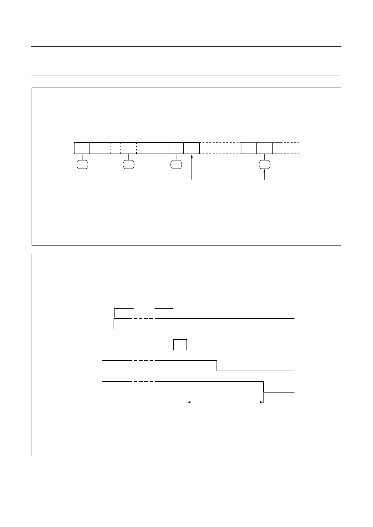
1999 Aug 19 98
Philips Semiconductors Objective Specification
Single-chip 8-bit microcontroller with CAN controller P8xC591
Fig.41 Simultaneous repeated START conditions from 2 Masters.
handbook, full pagewidth
MHI042
SWA SASPDATASLA
OTHER MST
CONTINUES
OTHER MASTER SENDS REPEATED
START CONDITION EARLIER
RETRY
SLA
08H
18H 28H 08H
Fig.42 Forces access to a busy I2C bus.
handbook, full pagewidth
MHI043
STA FLAG
STO FLAG
SDA LINE
SCL LINE
time limit
start condition
Page 99

1999 Aug 19 99
Philips Semiconductors Objective Specification
Single-chip 8-bit microcontroller with CAN controller P8xC591
15.2.15.3 I2C bus obstructed by a low level on SCL and
SDA
An I2C bus hang-up occurs if SDA or SCL is pulled LOW
by an uncontrolled source. If the SCL line is obstructed
(pulled LOW) by a device on the bus, no further serial
transfer is possible, and the SIO1 hardware cannot resolve
this type of problem. When this occurs, the problem must
be resolved by the device that is pulling the SCL bus line
LOW.
If the SDA line is obstructed by another device on the bus
(e.g., a slave device out of bit synchronization), the
problem can be solved by transmitting additional clock
pulses on the SCL line (see Figure 43). The SIO1
hardware transmits additional clock pulses when the STA
flag is set, but no START condition can be generated
because the SDA line is pulled LOW while the I2C bus is
considered free.
The SIO1 hardware attempts to generate a START
condition after every two additional clock pulses on the
SCL line. When the SDA line is eventually released, a
normal START condition is transmitted, state 08H is
entered, and the serial transfer continues.
If a forced bus access occurs or a repeated START
condition is transmitted while SDA is obstructed (pulled
LOW), the SIO1 hardware performs the same action as
described above. In each case, state 08H is entered after
a successful START condition is transmitted and normal
serial transfer continues. Note that the CPU is not involved
in solving these bus hang-up problems.
15.2.15.4 Bus error
A bus error occurs when a START or STOP condition is
present at an illegal position in the format frame. Examples
of illegal positions are during the serial transfer of an
address byte, a data or an acknowledge bit.
The SIO1 hardware only reacts to a bus error when it is
involved in a serial transfer either as a master or an
addressed slave. When a bus error is detected, SIO1
immediately switches to the not addressed slave mode,
releases the SDA and SCL lines, sets the interrupt flag,
and loads the status register with 00H. This status code
may be used to vector to a service routine which either
attempts the aborted serial transfer again or simply
recovers from the error condition as shown in Table 65.
Fig.43 Recovering from a bus obstruction caused by a low level on SDA.
handbook, full pagewidth
MHI044
STA FLAG
SDA LINE
SCL LINE
(1)(1)
(2) (3)
start
condition
(1) Unsuccessful attempt to send a Start condition.
(2) SDA line released.
(3) Successful attempt to send a Start condition; state D8H is centered.
Page 100

1999 Aug 19 100
Philips Semiconductors Objective Specification
Single-chip 8-bit microcontroller with CAN controller P8xC591
15.3 Software Examples of SIO1 Service Routines
This section consists of a software example for:
• Initialization of SIO1 after a RESET
• Entering the SIO1 interrupt routine
• The 26 state service routines for the
– Master transmitter mode
– Master receiver mode
– Slave receiver mode
– Slave transmitter mode
15.3.1 INITIALIZATION
In the initialization routine, SIO1 is enabled for both master
and slave modes. For each mode, a number of bytes of
internal data RAM are allocated to the SIO to act as either
a transmission or reception buffer. In this example, 8 bytes
of internal data RAM are reserved for different purposes.
The data memory map is shown in Figure 44. The
initialization routine performs the following functions:
• S1ADR is loaded with the parts own slave address and
the general call bit (GC)
• P1.6 and P1.7 bit latches are loaded with logic 1s
• RAM location HADD is loaded with the high-order
address byte of the service routines
• The SIO1 interrupt enable and interrupt priority bits are
set
• The slave mode is enabled by simultaneously setting
the ENS1 and AA bits in S1CON and the serial clock
frequency (for master modes) is defined by loading CR0
and CR1 in S1CON. The master routines must be
started in the main program.
The SIO1 hardware now begins checking the I2C bus for
its own slave address and general call. If the general call
or the own slave address is detected, an interrupt is
requested and S1STA is loaded with the appropriate state
information. The following text describes a fast method of
branching to the appropriate service routine.
15.3.2 SIO1 INTERRUPT ROUTINE
When the SIO1 interrupt is entered, the PSW is first
pushed on the stack. Then S1STA and HADD (loaded with
the high-order address byte of the 26 service routines by
the initialization routine) are pushed on to the stack.
S1STA contains a status code which is the lower byte of
one of the 26 service routines. The next instruction is RET,
which is the return from subroutine instruction. When this
instruction is executed, the high and low order address
bytes are popped from stack and loaded into the program
counter.
The next instruction to be executed is the first instruction
of the state service routine. Seven bytes of program code
(which execute in eight machine cycles) are required to
branch to one of the 26 state service routines.
SI PUSH PSW Save PSW
PUSH S1STA Push status code (low order
address byte)
PUSH HADD Push high order address byte
RET Jump to state service routine
The state service routines are located in a 256-byte page
of program memory. The location of this page is defined in
the initialization routine. The page can be located
anywhere in program memory by loading data RAM
register HADD with the page number. Page 01 is chosen
in this example, and the service routines are located
between addresses 0100H and 01FFH.
15.3.3 THE STATE SERVICE ROUTINE
The state service routines are located 8 bytes from each
other. Eight bytes of code are sufficient for most of the
service routines. A few of the routines require more than 8
bytes and have to jump to other locations to obtain more
bytes of code. Each state routine is part of the SIO1
interrupt routine and handles one of the 26 states. It ends
with a RETI instruction which causes a return to the main
program.
 Loading...