

Page 1

DATA SH EET
Preliminary specification
Supersedes data of 1995 Oct 11
File under Integrated Circuits, IC18
1996 Jun 19
INTEGRATED CIRCUITS
P82C150
CAN Serial Linked I/O device
(SLIO) with digital and analog port
functions
Page 2

Philips Semiconductors Preliminary specification
CAN Serial Linked I/O device (SLIO) with
digital and analog port functions
P82C150
1996 Jun 19 2
CONTENTS
1 FEATURES
2 GENERAL DESCRIPTION
3 ORDERING INFORMATION
4 BLOCK DIAGRAM
5 FUNCTIONAL DIAGRAM
6 PINNING INFORMATION
6.1 Pinning
6.2 Pin description
7 FUNCTIONAL DESCRIPTION
7.1 I/O functions
7.2 I/O registers
7.3 CAN functions
7.4 Initialization
7.5 P82C150 operation after RESET or change of
bus mode
8 LIMITING VALUES
9 DC CHARACTERISTICS
10 AC CHARACTERISTICS
11 APPLICATION INFORMATION
11.1 Maximum bus length
11.2 Start up sequence
11.3 External oscillator mode
11.4 Using digital I/O port functions
11.5 Using DPM
11.6 Using ADC
11.7 Using analog input port functions
11.8 CAN-bus system applications
12 PACKAGE OUTLINE
13 SOLDERING
13.1 Introduction
13.2 Reflow soldering
13.3 Wave soldering
13.4 Repairing soldered joints
14 DEFINITIONS
15 LIFE SUPPORT APPLICATIONS
Page 3

1996 Jun 19 3
Philips Semiconductors Preliminary specification
CAN Serial Linked I/O device (SLIO) with
digital and analog port functions
P82C150
1 FEATURES
• Single-chip I/O device with CAN protocol controller
• Meets CAN protocol specification version 2.0 A and B
(passive) with restricted bit timing
• Fully integrated clock oscillator (no crystal required)
• 16 configurable digital or analog I/O port pins
• Each of the port pins individually configurable via
CAN-bus: port direction, port mode and event capture
facilities for inputs (event driven or polling)
• Up to sixteen digital inputs; automatic transmission of a
CAN message on a change on inputs individually
selectable
• Up to sixteen 3-state outputs
• Up to two quasi-analog outputs with 10-bit accuracy
• 10-bit analog-to-digital converter with up to six
multiplexed analog input channels (for accuracy see
Section 11.6)
• Two general purpose comparators
• Bit rate from 20 kbit/s up to 125 kbit/s using internal
oscillator
• Automatic bit rate detection and calibration
• Up to sixteen P82C150 nodes for one CAN-bus system
• Four identifier bits programmable
• SLIO functions controlled by a single intelligent node
(‘host’)
• Sleep-mode with wake-up via CAN-bus
• Differential CAN-bus input comparator and CAN-bus
output driver
• Supply voltage: 5 V ±4%
• Operating temperature: two ranges −40 to +85 °C and
−40 to +125 °C.
2 GENERAL DESCRIPTION
The P82C150 is a single-chip 16-bit I/O device including a
Controller Area Network (CAN) protocol controller with
automatic bit rate detection and calibration. It features 16
configurable I/O port pins with programmable direction,
digital and analog modes.
The P82C150 provides a configurable event capture
facility supporting automatic transmission caused by a
change on the port input pins.
The clock oscillator requires no external components,
thus, the cost of the CAN link is reduced significantly.
The P82C150 is a very cost-effective way to increase the
I/O capability of a microcontroller based CAN node as well
as to reduce the amount and complexity of wiring.
Advanced safety is provided by the CAN protocol.
Applications:
• Body electronics and instrumentation in automotive
applications
• Sensor/actuator interface in automotive and general
industrial applications
• Extension of I/O capabilities of microcontroller based
CAN nodes.
3 ORDERING INFORMATION
TYPE NUMBER
PACKAGE
TEMPERATURE
RANGE (°C)
NAME DESCRIPTION VERSION
P82C150 AFT
SO28 plastic small outline package; 28 leads; body width 7.5 mm SOT136-1
−40 to +85
P82C150 AHT −40 to +125
Page 4
1996 Jun 19 4
Philips Semiconductors Preliminary specification
CAN Serial Linked I/O device (SLIO) with
digital and analog port functions
P82C150
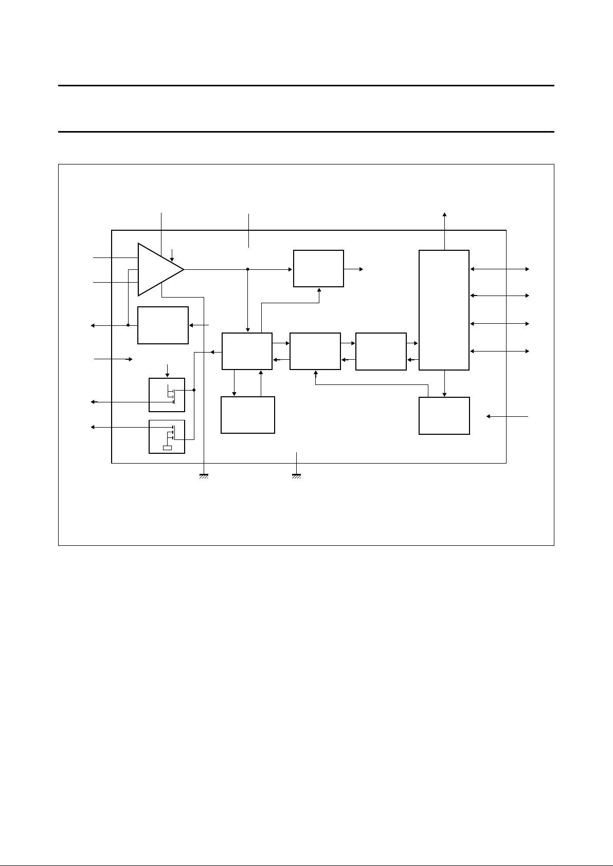
4 BLOCK DIAGRAM
Fig.1 Block diagram.
handbook, full pagewidth
P82C150
ERROR
MANAGEMENT
LOGIC
RXO
21
RX1
22
19
18
BIT STREAM
PROCESSOR
input
comparator
TRANSMIT/
RECEIVE
LOGIC
PORT
LOGIC
IDENTIFIER
LATCH
23
4
20
OSCILLATOR
AND
CALIBRATOR
clock
8
REF
AV
DD
V
DD
+5 V
+5 V
9 to 16
5, 6, 7
1, 2, 3
P8 to P15
P5 to P7
P2 to P4
P0/CLK, P1
AV
SS
MHA064
CAN-bus
CAN-bus
17
P16
XMOD
25
26TX1
TX0
RST
16 I/O
port pins
1
/2 AV
DD
+
REFERENCE
VOLTAGE
27, 28
bus mode
bus mode
I/O
REGISTERS
24
V
SS
Page 5
1996 Jun 19 5
Philips Semiconductors Preliminary specification
CAN Serial Linked I/O device (SLIO) with
digital and analog port functions
P82C150
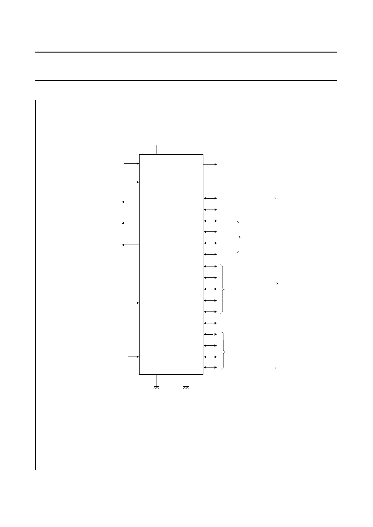
5 FUNCTIONAL DIAGRAM
Fig.2 Functional diagram.
handbook, full pagewidth
P82C150
REF
RX0
RX1
TX0
P15
P13
P14
P12
P11
P10
P9
P8
P7
P6
P5
P4
P3
P2
P1
P0/CLK
RST (reset)
XMOD
CAN-bus inputs
analog-to-digital
comparator input
comparator
inputs
16-bit
digital I/O
MHA066
TX1
P16
CAN-bus outputs
ADC feedback output
multiplexed analog-
to-digital signal
analog
input
DPM1
output
analog inputs,
analog switches
DPM2
output
identifier
programming
reference
voltage output
VSS
AVSS
VDD
AVDD
Page 6
1996 Jun 19 6
Philips Semiconductors Preliminary specification
CAN Serial Linked I/O device (SLIO) with
digital and analog port functions
P82C150
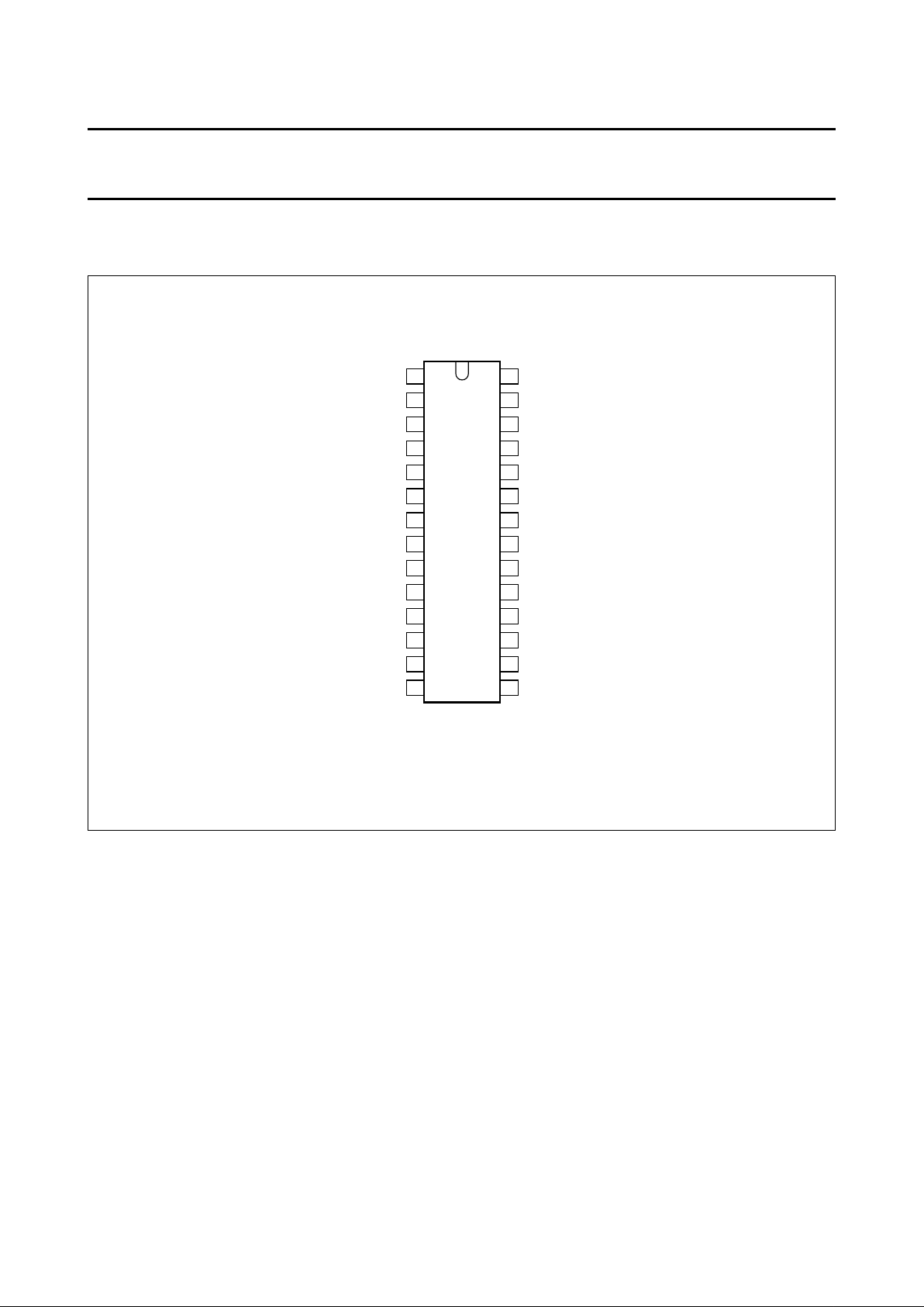
6 PINNING INFORMATION
6.1 Pinning
Fig.3 Pin configuration.
handbook, halfpage
26
27
24
23
22
21
20
19
18
17
16
15
1
2
3
4
5
6
7
8
9
10
11
12
13
P82C150
14
28
25
MHA065
P2
P3
P4
V
SS
XMOD
P6
P5
P7
V
DD
P8
P9
P10
P11
P12
P13
P1
P0/CLK
TX1
AV
SS
TX0
RST
RX1
RX0
AV
DD
REF
P16
P15
P14
Page 7

1996 Jun 19 7
Philips Semiconductors Preliminary specification
CAN Serial Linked I/O device (SLIO) with
digital and analog port functions
P82C150
6.2 Pin description
Table 1 Pin description for P82C150; SO28; see note 1
Note
1. In this documentation the port pins are referred to by their symbols, not by their pin number. For example P15 means
I/O Port 15 at pin 16.
SYMBOL PIN DESCRIPTION
P2 1 I/O Ports P2 to P3; Identifier programming input.
P3 2
P4 3 I/O Port 4; DPM2 output.
V
SS
4 Ground, digital part (0 V; logic circuits and CAN-bus driver).
P5 5 I/O Ports P5 to P6; analog input.
P6 6
P7 7 I/O Port 7; analog input or analog-to-digital comparator 1 output.
V
DD
8 Power supply, digital part (+5 V; logic circuits and CAN-bus driver).
P8 9 I/O Port 8; analog input or comparator 3 output.
P9 10 I/O Port 9; analog input or comparator 2 output.
P10 11 I/O Port 10; comparator 3 inverting input or DPM1 output.
P11 12 I/O Port 11; comparator 3 non-inverting input.
P12 13 I/O Port 12; comparator 2 inverting input.
P13 14 I/O Port 13; comparator 2 non-inverting input.
P14 15 I/O Port 14; multiplexed analog signal.
P15 16 I/O Port 15; analog-to-digital comparator input.
P16 17 Feedback output of analog-to-digital converter.
AV
DD
18 Power supply, analog part (+5 V; CAN input, oscillator and reference).
REF 19 Reference voltage output (
1
⁄2× AVDD).
AV
SS
20 Ground, analog part (0 V; CAN input, oscillator, reference).
RX0 21 CAN-bus input.
RX1 22
RST 23 External reset input (active-HIGH) for internal oscillator mode; pulled to +5 V for external
oscillator mode (see Section 11.3).
XMOD 24 Connected to GND for internal oscillator mode; external reset input (active-LOW) for
external oscillator mode (see Section 11.3).
TX0 25 Open-drain CAN-bus output: dominant = LOW; recessive = floating.
TX1 26 Open-drain CAN-bus output: dominant = HIGH; recessive or at bus mode 2 floating.
P0/CLK 27 I/O Port P0, Identifier programming input in internal oscillator mode; clock input in external
oscillator mode (see Section 11.3).
P1 28 I/O Port P1; identifier programming input.
Page 8
1996 Jun 19 8
Philips Semiconductors Preliminary specification
CAN Serial Linked I/O device (SLIO) with
digital and analog port functions
P82C150
7 FUNCTIONAL DESCRIPTION
7.1 I/O functions
The P82C150 provides 16 port pins (P15 to P0) which are
individually configurable via CAN-bus. Besides the digital
I/O functions some of these port pins provide analog I/O
functions.
7.1.1 D
IGITAL INPUT FUNCTIONS
Input levels HIGH and LOW on the port pins (P15 to P0)
can be read in two ways by the host node:
• Polling: a Remote Frame is sent to the P82C150 to be
answered by a Data Frame containing the Data Input
Register contents.
• Event capture: in case of edge-triggered mode, the
P82C150 sends the same Data Frame caused by the
event of a rising and/or falling edge on the
corresponding port pins (see Table 3).
7.1.2 D
IGITAL OUTPUT FUNCTIONS
The Data Output Register is set via a CAN message.
Its content is only output when the corresponding bits of
the Output Enable Register are set to logic 1s.
7.1.3 A
NALOG INPUT/OUTPUT FUNCTIONS
• Up to six multiplexed analog input signals for
analog-to-digital conversion or general purpose
• Up to two quasi-analog output channels (DPM;
Distributed Pulse Modulation)
• Two input comparators, for example for window
comparator applications
• A separate analog-to-digital input comparator with
feedback output.
Analog-to-digital converted digital results are obtained by
reading the Analog-to-Digital Conversion (ADC) Register.
Analog functions of each port pin are individually
controlled by the Analog Configuration Register.
Writing the I/O registers is done serially via CAN-bus by
Data Frames. The first data byte contains the register
address, and the second and third data bytes represent
the register contents. If a read only register is addressed,
the contents of the second and third data bytes are
ignored.
It is recommended to set unused port pins to HIGH
(100 kΩ resistor to V
DD
).
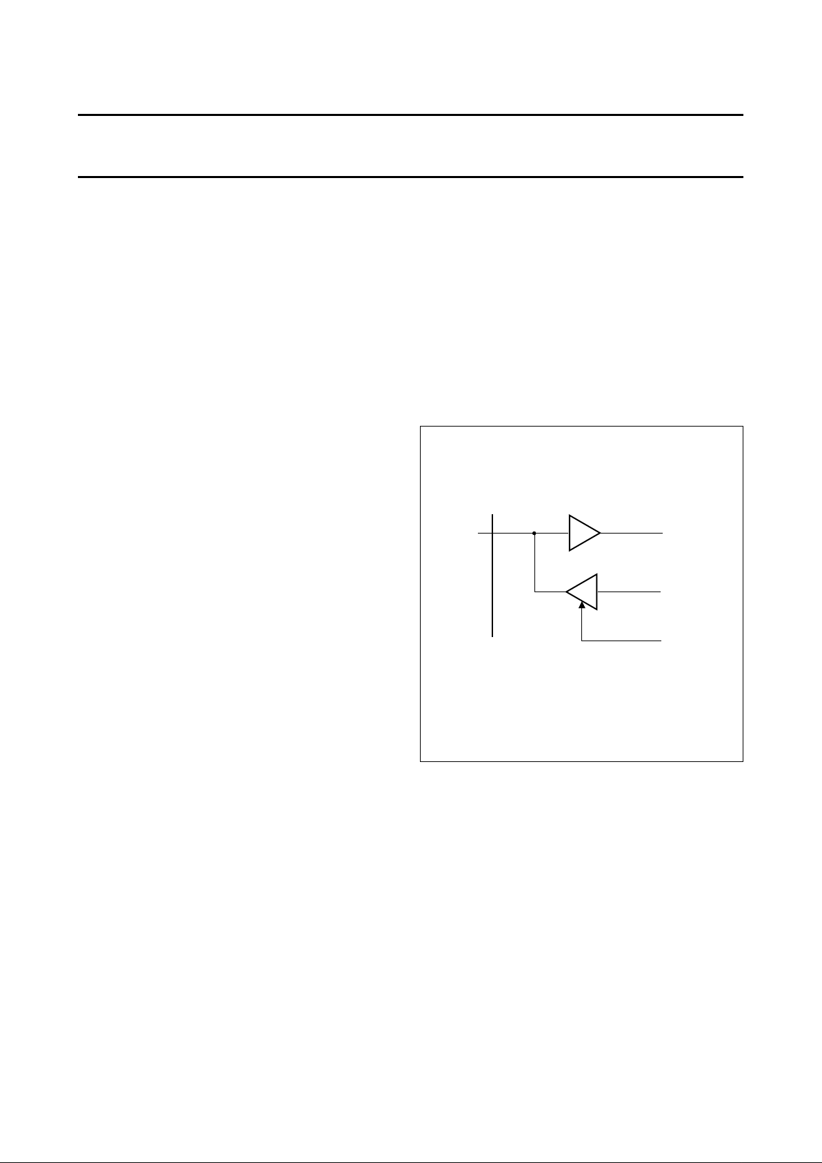
Fig.4 I/O port pins.
handbook, halfpage
Px
MHA068
DIx
DOx
OEx
3-state buffer
P82C150
Page 9

1996 Jun 19 9
Philips Semiconductors Preliminary specification
CAN Serial Linked I/O device (SLIO) with
digital and analog port functions
P82C150
7.2 I/O registers
Table 2 I/O register map
15
(MSB)
1413121110987654321
0
(LSB)
ADDRESS 0: DATA INPUT
DI15 DI14 DI13 DI12 DI11 DI10 DI9 DI8 DI7 DI6 DI5 DI4 DI3 DI2 DI1 DI0
ADDRESS 1: POSITIVE EDGE
PE15 PE14 PE13 PE12 PE11 PE10 PE9 PE8 PE7 PE6 PE5 PE4 PE3 PE2 PE1 PE0
ADDRESS 2: NEGATIVE EDGE
NE15 NE14 NE13 NE12 NE11 NE10 NE9 NE8 NE7 NE6 NE5 NE4 NE3 NE2 NE1 NE0
ADDRESS 3: DATA OUTPUT
DO15 DO14 DO13 DO12 DO11 DO10 DO9 DO8 DO7 DO6 DO5 DO4 DO3 DO2 DO1 DO0
ADDRESS 4: OUTPUT ENABLE
OE15 OE14 OE13 OE12 OE11 OE10 OE9 OE8 OE7 OE6 OE5 OE4 OE3 OE2 OE1 OE0
ADDRESS 5: ANALOG CONFIGURATION
ADC OC3 OC2 OC1 0 M3 M2 M1 SW3 SW2 SW1 0 0 0 0 0
ADDRESS 6: DPM1
DP9DP8DP7DP6DP5DP4DP3DP2DP1DP0000000
A
DDRESS 7: DPM2
DQ9DQ8DQ7DQ6DQ5DQ4DQ3DQ2DQ1DQ0000000
A
DDRESS 8: ANALOG-TO-DIGITAL CONVERSION (ADC)
AD9 AD8 AD7 AD6 AD5 AD4 AD3 AD2 AD1 AD0 0 0 0 0 0 0
Page 10

1996 Jun 19 10
Philips Semiconductors Preliminary specification
CAN Serial Linked I/O device (SLIO) with
digital and analog port functions
P82C150
7.2.1 DATA INPUT REGISTER (ADDRESS 0)
This read only register contains the states of port pins
P15 to P0 which are transmitted on request, or
automatically by change of one of the input levels,
provided that the respective input is configured to event
capture mode (see Table 3). When an edge is detected
the port state is loaded into the transmit buffer after the
Control Field of the triggered message is sent. Therefore a
delay for input settling is provided. If between edge
detection and transmission of the data input register
another input signal change at the input port occurs, the
corresponding data input register bit is overwritten by the
current input port value. Additionally the register content is
sent automatically after wake-up or bus mode change,
once the bit time has been calibrated (part of the ‘sign-on’
message).
7.2.2 P
OSITIVE EDGE REGISTER (ADDRESS 1)
This write only register contains configuration information
per port pin for the event capture facility.
The corresponding PE-bit (see Table 3) has to be set to
logic 1 to enable capturing of the rising edge.
7.2.3 N
EGATIVE EDGE REGISTER (ADDRESS 2)
This write only register contains configuration information
per port pin for the event capture facility.
The corresponding NE-bit (see Table 3) has to be set to
logic 1 to enable capturing of the falling edge.
The combination of PE and NE functions is possible.
7.2.4 D
ATA OUTPUT REGISTER (ADDRESS 3)
This write only register contains the output data for the port
pins. The output drivers are bitwise enabled by OE
(see Section 7.2.5). New data for the output port register
are processed and written to the output ports directly after
the corresponding CAN message to the P82C150 is
successfully checked and becomes valid.
7.2.5 O
UTPUT ENABLE REGISTER (ADDRESS 4)
This write only register controls the output drivers of the
port pins. The corresponding Output Enable Register bit
has to be set to logic 1 to enable an output driver. If set to
logic 0, the corresponding output driver is disabled
(floating; see Fig.7).
Table 3 Programming of the I/O registers to event capture on edge or to digital output
X = don’ t care; n=0to15.
FUNCTION
REGISTER CONTENTS OF PARTICULAR PORT PIN
POSITIVE EDGE
(BITS PEn)
NEGATIVE EDGE
(BITS NEn)
OUTPUT ENABLE
(BITS OEn)
Digital output X X 1
Digital input
Polling X X X
Event capture on edge
Rising 1 0 X
Falling 0 1 X
Rising and Falling 1 1 X
Page 11

1996 Jun 19 11
Philips Semiconductors Preliminary specification
CAN Serial Linked I/O device (SLIO) with
digital and analog port functions
P82C150
7.2.6 ANALOG CONFIGURATION REGISTER (ADDRESS 5)
This read/write register contains the bits ADC, OC3 to
OC1, M3 to M1 and SW3 to SW1 (see Fig.7).
• ADC bit (analog-to-digital conversion start bit; write only
bit). The P82C150 starts an analog-to-digital conversion
cycle at ADC = 1 ended with the transmission of a
message containing the result. After that, the ADC bit is
reset automatically.
• OC3 to OC1 bits (comparator output data; read only
bits). The bits OC3 to OC1 represent the logical output
level of the analog comparators at input port pins P10,
P11, P12, P13 and P15. The P82C150 sends back the
logical output value of these comparators after having
received a Data Frame (see Section 7.3.3) addressing
the Analog Configuration Register. The comparator
outputs can be monitored at the output port pins P8, P9
and P7.
• M3 to M1 bits (multiplexer control bits; write only bits).
The logical value of the comparators is monitored on
port pins P8, P9 and P7 (see Fig.7) by setting M3 to M1
to logic 1, provided that these pins are configured as
outputs (OE = 1). Additionally the register content is
sent automatically when the corresponding port bits in
the Positive Edge Register and/or Negative Edge
Register and the corresponding bits in the Output
Enable Register are set.
• SW3 to SW1 (analog switch control bits; write only bits).
One of the analog switches S1 to S6 can be closed by
setting the switch bits to the corresponding value
(see Fig.7 and Table 4).
Table 4 Analog switch selection by SW3, SW2, SW1.
Note
1. Evidently if P14 is driven, it may not be connected to
any other driven pin via the internal analog switches
(avoid short-circuit!).
SW3 SW2 SW1 SWITCH STATE
0 0 0 no switch closed (S0); note 1
0 0 1 S1 closed
0 1 0 S2 closed
0 1 1 S3 closed
1 0 0 S4 closed
1 0 1 S5 closed
1 1 0 S6 closed
1 1 1 reserved
7.2.7 DPM1 REGISTER (ADDRESS 6)
This write only register contains data for a quasi-analog
output signal on port pin P10, which is generated by
Distributed Pulse Modulation (DPM; see Fig.9).
The Output Enable bit must be set for this functions
(OE10 = 1). The DPM1 output signal is inverted by setting
DO10 = 1. The number of output pulses during a DPM
period is given by the DPM1 Register value. These pulses
have 4 × t
CLK
length and are distributed over the DPM
period. An analog voltage is provided after smoothing the
output signal by an external RC combination.
7.2.8 DPM2 R
EGISTER (ADDRESS 7)
This write only register contains data for a quasi-analog
output signal on port pin P4. The function of the DPM2
corresponds to the definition of DPM1.
7.2.9 A
NALOG-TO-DIGITAL CONVERSION (ADC)
R
EGISTER (ADDRESS 8)
This read only register contains the result of the
analog-to-digital converted level of that I/O pin which was
selected by the SW bits. The conversion is started by
ADC-bit set to logic 1 (see Section 7.2.6), or by
transmitting a Data Frame addressing the ADC Register.
Page 12

1996 Jun 19 12
Philips Semiconductors Preliminary specification
CAN Serial Linked I/O device (SLIO) with
digital and analog port functions
P82C150
Fig.5 Analog configuration of I/O port pins; R1, R2 and C1 are used to implement the analog-to-digital converter.
k, full pagewidth
15
3
P82C150
7
6
5
9
10
16
17
R1
R2
C1
1
/4f
CLK
ADC
REGISTER
OC1
S0
S2
S3
S4
S5
S6
P13
13
12
11
DPM1
DPM2
OC2
OC3
M3
M2
M1
MHA067
P16
P15
P14
P7
P6
P5
P8
P9
14
P12
P11
P10
P4
S1
SW3 to SW1
= 1
= 1
1
/2 V
DD
DO7
DO8
DO9
DO4
DO10
OE7
OE8
OE9
OE10
OE4
+
−
+
−
+
−
Page 13

1996 Jun 19 13
Philips Semiconductors Preliminary specification
CAN Serial Linked I/O device (SLIO) with
digital and analog port functions
P82C150
Fig.6 DPM output pulses at DO10(4) = 0; output pulses are inverted at DO10(4) = 1.
handbook, full pagewidth
L
H
L
H
L
H
L
H
L
H
L
H
L
H
t
DPM
= 1024 x 4 t
CLK
4 t
CLK
DPM = 0
DPM = 1
DPM = 2
DPM = 3
DPM = 512
DPM = 513
DPM = 1023
MHA081
Distributed Pulse Modulation (DPM) is a special pulse count modulation.
Page 14

1996 Jun 19 14
Philips Semiconductors Preliminary specification
CAN Serial Linked I/O device (SLIO) with
digital and analog port functions
P82C150
7.3 CAN functions
The P82C150 meets the CAN protocol specification
version 2.0 A and B (passive) with restricted bit timing
because of the on-chip RC-oscillator and the automatic bit
rate detection.
In a system with P82C150 nodes there must be at least
one conventional crystal-driven CAN controller (host node)
which is compatible to the CAN specification V1.2 or later
to control P82C150 nodes. Host nodes compatible to CAN
specification V1.1 can also be used provided that the
P82C150 nodes are powered by a high-accuracy power
supply or they are in external oscillator mode (refer to
Section 11.3).
Each time a P82C150 node receives a Data Frame, it
initiates the transmission of a Data Frame containing four
bits status information, the register address (previously
received) and the current contents of the addressed
register (exception: see Section 7.3.3.1). This enables the
host node to verify that the addressed register has
correctly been written in case of writeable registers, and to
read the contents in case of readable registers.
7.3.1 CAN IDENTIFIER
Data and Remote Frames to be processed by the
P82C150 are of Standard Format with 11 Identifier bits
ID.10 to ID.0. Frames with extended Identifier (CAN
specification version 2.0 B) are ignored.
The way of identifier programming is based on two facts:
• Each P82C150 operates with only two Identifiers
distinguished by the LSB (see Tables 5, 6 and 7).
The identifier with the higher priority is used for Data
Frame reception. An extra Identifier is used for
calibration purposes.
• There can be maximum sixteen P82C150 circuits in one
network.
Table 5 Message types and format
Note
1. DLC = Data Length Code; DIR = LSB of Identifier (see Section 7.3.1).
Table 6 Standard Format Identifier bits ID.10 to ID.0
1 = recessive; 0 = dominant
Table 7 Description of the Standard Format Identifier bits
FRAME TRANSMISSION BY 82C150 RECEPTION AT 82C150
Data Frame yes (DLC = 3; DIR = 1) yes (DLC = 3; DIR = 0; calibration message
with DLC = 2 to 8 allowed, see Section 7.3.10)
Remote Frame no yes (DLC = 3; DIR = 1)
Error Frame yes yes
Overload Frame yes (only as a response) yes
IDENTIFIER
ID.10 ID.9 ID.8 ID.7 ID.6 ID.5 ID.4 ID.3 ID.2 ID.1 ID.0
0 1 P3 1 0 P2 P1 P0 1 0 DIR RTR
BIT SYMBOL DESCRIPTION
ID.8 P3 Programmable identifier bits read from Port pins P3 to P0 during reset. The input levels
on P3 to P0, for example set by resistors to V
SS
or to VDD, are latched in the Identifier
latch with the falling edge of the RST input signal. They represent the variable part of
the Identifier, while the remaining bits are fixed (mask-programmed), P3 to P0 can be
used as I/O ports after reset.
ID.5 to ID.3 P2 to P0
ID.0 DIR DIR = 1 for transmission of Data Frames to the host. It must be set to a logic 1 in
Remote Frames and to a logic 0 in Data Frames received from the host.
RTR Remote Transmission Request bit.
Page 15

1996 Jun 19 15
Philips Semiconductors Preliminary specification
CAN Serial Linked I/O device (SLIO) with
digital and analog port functions
P82C150
7.3.2 TRANSMISSION OF DATA FRAMES
Data Frames transmitted by the P82C150 contain three
data bytes (see Fig.7). The first data byte contains the
status information and the register address A3 to A0 (see
Tables 8 and 9), the other two data bytes contain the
content of the addressed I/O Register.
After each successful message transmission, the
P82C150 delays the transmission of a possibly further
pending message for three bit times. The reason is to give
other CAN controllers - with a lower identifier priority - the
possibility to transmit a message in case of faulty contact
at one of the edge-triggered port pins.
7.3.3 R
ECEPTION OF DATA FRAMES AND REMOTE
FRAMES
Received Data Frames have the same format as
transmitted ones, only the DIR-bit (ID.0) in the Arbitration
Field is different. The status bits RSTD, EW, BM1 and BM0
are ignored during reception.
The P82C150 confirms each reception of a Data Frame by
transmitting a Data Frame containing the (new) contents of
the addressed I/O Register.
7.3.3.1 Exceptions to the rule
1. Analog Configuration Register: If a P82C150 receives
a Data Frame addressing the Analog Configuration
Register and the ADC bit is set to logic 1, it will
respond with two messages. The first message returns
the contents of the Analog Configuration Register. The
control instructions are executed (e.g. next analog
input channel selected), and an analog-to-digital
conversion cycle is started after a set-up time. After
finishing the analog-to-digital conversion cycle, the
second message is transmitted containing the result
(ADC Register).
2. ADC Register: On receiving a Data Frame addressing
the ADC Register, the P82C150 starts an
analog-to-digital conversion cycle. It automatically
returns the result of the conversion (ADC Register) by
transmitting a respective Data Frame after finishing
the analog-to-digital conversion cycle.
3. At normal operation, the calibration messages are
confirmed by returning a dominant bit in the
acknowledge slot. There is no particular confirmation
message returned by the P82C150. Only after
entering the calibrated state (start-up), a Data Frame
(‘sign-on’ message) containing the Data Input Register
contents is transmitted indicating to the host node, that
the P82C150 is now ready for transmission.
7.3.3.2 Remote Frame
Received Remote Frames must have the Data Length
Code DLC = 3 (Remote Frames with DLC≠ 3 are ignored).
It is answered by a Data Frame containing the contents of
the Data Input Register.
Page 16

1996 Jun 19 16
Philips Semiconductors Preliminary specification
CAN Serial Linked I/O device (SLIO) with
digital and analog port functions
P82C150
Table 8 Data Frame Byte 1
Table 9 Description of Data Frame Byte 1 bits
STATUS REGISTER ADDRESS
RSTD EW BM1 BM0 A3 A2 A1 A0
SYMBOL DESCRIPTION
Status
RSTD It is logic 1 in the first message (‘sign-on’ message) after the successful detection of the bit rate
(bit time calibrated).
EW Logic 1, if the error warning limit (32) is reached. In the “sign-on” message EW is always logic 1. The
EW status bit is set when the Receive Error Counter or the Transmit Error Counter have exceeded the
Error Warning Limit of 32, also temporarily, since the last successful transmission of a message.
BM1 Bus mode status bits.
BM0
Register address
A3 to A0 Register address bits.
Fig.7 P82C150 Data Frame.
handbook, full pagewidth
MHA071
0 0 1 P3 1 0 P2 P1 P0 1 0 DIR RTR
ID0ID10
SOF
Identifier
0 0 0 0 1 1 RSTD EW BM1 BM0 A3 A2 A1 A0
reserved Data Length Code P82C150 status register address
X X X X X X X X X X X X X X X X
I/O Register data(15 to 8) I/O Register data(7 to 0)
CONTROL FIELD
ARBITRATION FIELD
BYTE 1
BYTE 2 BYTE 3
SOF: Start Of Frame.
RTR: Remote Transmission Request.
P3 toP0: equals programmed identifier bits.
Page 17

1996 Jun 19 17
Philips Semiconductors Preliminary specification
CAN Serial Linked I/O device (SLIO) with
digital and analog port functions
P82C150
7.3.4 CAN-BUS MODES
The P82C150 can pass through four CAN-bus modes
under certain conditions (see Fig.8). In the bus modes
0 to 2 (see Table 10) the P82C150 is operating with
different input comparator configurations. Bus mode 3 is
the power reduced Sleep Mode.
The bus modes support:
• Communication on two balanced wires (differential
system)
• Communication on one wire in a two-wire differential
system
• Sleep Mode with wake-up via either a dominant signal
on RX0 or RX1 input
• Connection of a second transmission medium
(redundancy)
There are two possibilities for condition 1 to switch to the
next mode (see Fig.8):
• Overflow of the bit counter when 8192 is reached since
the last calibration message
• Overflow of the Transmit Error Counter (>255; bus-off
limit reached).
When the bus mode changes, all I/O Registers are cleared
and outputs become floating (OE bits cleared). That
means the I/O ports return to a fail-safe state whenever the
P82C150 looses connection to its host controller. This is a
kind of network watchdog function. The status bits are set
to the following values after a bus mode change:
• RSTD = 1
• EW = 0
• BM
new
=BM
old
+1.
The programmed Identifier bits remain unchanged.
After reset the P82C150 changes directly into bus mode 3
(Sleep Mode). During Sleep Mode, the internal RC
oscillator is stopped, and all the output drivers are disabled
(I/O Register contents cleared). A P82C150 in Sleep Mode
can be woken up via CAN-bus lines (dominant level on
RX0 or RX1) or by a reset condition.
Fig.8 CAN-bus modes and switch-over conditions.
olumns
DIFFERENTIAL
MODE
Inputs: RX0, RX1
Outputs: TX0, TX1
'0'
ONE-WIRE
RX1 MODE
Input: RX1
Outputs: TX0, TX1
'1'
'2'
SLEEP
MODE
Inputs: RX0, RX1
Outputs: no
'3'
ONE-WIRE
RX0 MODE
Input: RX0
Output: TX0
Condition 1
Condition 1
Condition 1
Condition 2
MHA070
end of
RESET
Condition 1:
bit counter overflow (>8191) or Transmit Error Counter overflow (>255).
Condition 2:
dominant bit detected on RX0 and RX1.
Table 10 Can-bus modes
Note
1. Output TX1 is disabled in bus mode 2 to tolerate short-circuit between the CAN-bus wires CAN_H and CAN_L.
BUS MODE
BITS RECEPTION LEVEL TRANSMISSION
BM1 BM0 RECESSIVE DOMINANT TX1 TX0
0 = Differential 0 0 RX0 > RX1 RX0 < RX1 enabled enabled
1 = One-wire RX1 0 1 RX1 < REF RX1 > REF enabled enabled
2 = One-wire RX0 1 0 RX0 > REF RX0 < REF disabled enabled
3 = Sleep 1 1 RX0 > REF
and
RX1 < REF
RX0 < REF
or
RX1 > REF
disabled disabled
Page 18

1996 Jun 19 18
Philips Semiconductors Preliminary specification
CAN Serial Linked I/O device (SLIO) with
digital and analog port functions
P82C150
7.3.5 BIT TIMING
The Nominal Bit Time of the P82C150 is subdivided into 10
Time Quanta. The Synchronization Time Segment
(SYNC_SEG) and the Propagation Time Segment
(PROP_SEG) are each one Time Quantum long. The
Phase Buffer Segment 1 (PHASE_SEG1) and the Phase
Buffer Segment 2 (PHASE_SEG2) are each four Time
Quanta long. The Resynchronization Jump Width (SJW) is
four Time Quanta long.
The sample point is located at the end of the Phase Buffer
Segment 1. The Nominal Bit Time is internally adjusted to
that bit timing which is provided by the crystal driven host
(calibration message).
The usable bus length at a given bit rate is reduced in
comparison to other CAN controllers with programmable
bit timing because the Propagation Time Segment is fixed
to
1
⁄10 length of the Nominal Bit Time. The bit segmentation
of the crystal driven host should be programmed like the
fixed bit segmentation of the P82C150, e.g. one bit time
segment is1⁄10 length of the Nominal Bit Time (refer also
to Table 15 for bit time programming).
Table 11 Bit time subdivision
1 BIT TIME
BT1 BT2 BT3 BT4 BT5 BT6 BT7 BT8 BT9 BT10
SYNC_SEG PROP_SEG
PHASE_SEG1 PHASE_SEG2
7.3.6 CAN-BUS TRANSCEIVER
The transceiver of the P82C150 consists of the
configurable input comparator and of complementary
open-drain driver outputs. The reference voltage REF is
an additional output.
7.3.6.1 CAN-bus input comparator (RX0, RX1)
The input comparator monitors the transient voltage on
RX1 and RX0.
The result of the input comparator is logic 1 if the voltage
levels of the CAN-bus lines are regarded as recessive, and
logic 0 if they are regarded as dominant.
The recessive state and the dominant state are not
equivalent and may not be mixed-up.
The input comparator is configurable depending on the
four CAN-bus modes (see Table 10), supporting
battery-powered applications (Sleep Mode) and tolerance
against bus wiring failures.
7.3.6.2 CAN-bus output drivers (TX0, TX1)
The output driver function is shown in Table 12. The output
driver TX1 is disabled in bus mode 2 to tolerate a
short-circuit between the CAN-bus lines in a two-wire
differential CAN physical layer.
Table 12 CAN-bus driver output function
CAN OUTPUT RECESSIVE
DOMINANT
RESET STATE, BUS-OFF AND
SLEEP MODE (MODE 3)
MODES 0 AND 1 MODE 2
TX0 floating LOW LOW floating
TX1 floating HIGH floating floating
Page 19

1996 Jun 19 19
Philips Semiconductors Preliminary specification
CAN Serial Linked I/O device (SLIO) with
digital and analog port functions
P82C150
7.3.7 TRANSMIT AND RECEIVE LOGIC
The transmit and receive logic stores the destuffed bit
stream which was received or is about to be transmitted.
The incoming Identifier is compared with that of the
P82C150. The content of the message is transferred to the
port logic in case of matching.
At transmission, the message about to be sent is put
together: the Identifier, the status information, the register
address and the content of the addressed register from the
port logic.
7.3.8 B
IT STREAM PROCESSOR AND ERROR
MANAGEMENT LOGIC
The Bit Stream Processor (BSP) is a sequencer to control
the data stream between the transmit/receive logic
(parallel data) and the on-chip CAN transceiver (serial
data). Reception/transmission, bit stuffing/destuffing,
arbitration and error detection, according to CAN protocol
specification version 2.0 A and B (passive), are performed.
Further, automatic re-transmission of corrupted messages
is handled by means of continuously comparing the output
bit stream with the input bit stream. Moreover, the Bit
Stream Processor provides control information to calibrate
the internal bit time.
The Error Management Logic is responsible for the
complete CAN-inherent error management.
7.3.9 O
SCILLATOR AND CALIBRATION
The P82C150 contains an on-chip RC-oscillator. The bit
time is automatically calibrated by messages being
received via CAN-bus. During start-up (after wake-up or
reset) any message is used to calibrate the bit time until
the calibration is sufficient to receive messages correctly.
From this time on, the bit time is calibrated and fine-tuned
by calibration messages with a special Identifier
transmitted by the crystal-controlled host.
Only P82C150 nodes being calibrated by calibration
messages can transmit messages. The first message is
transmitted directly after entering the calibrated state
(‘sign-on’ message). Since the P82C150 is not able to
transmit as long as the bit time is not calibrated, it cannot
wake-up other CAN nodes via the bus line. Hence to keep
the network alive, the calibration message must be
transmitted regularly by a crystal-controlled (host) node
with a maximum repetition period of 8192 bit (bit length
measured by the 82C150). It is recommended to select a
repetition period between 3800 and maximum 8000 bit
times.
7.3.10 C
ALIBRATION MESSAGE
The calibration message has to meet the following
requirements
• Transmitted by a crystal-controlled node (host node)
• Identifier: 000 1010 1010 (1 = recessive; 0 = dominant)
• RTR bit: 0
• Allowed control field: DLC=2to8
• The first recessive to dominant transition after the
control field must be followed by another recessive to
dominant transition in a distance of exactly 32 bit (stuff
bits included).
Example of a suitable calibration message (there are
others using different data bytes; see Table 13):
• Data length code: 0010
• 1st data byte: 1010 1010 (AAH)
• 2nd data byte: 0000 0100 (04H).
Table 13 Example of a suitable calibration message
The two important 1/0 transitions are marked by underlines; see note 1.
Note
1. I = stuff bit (recessive); the total length is 67 bit from start-of-frame to end-of-intermission.
SOF ARBITRATION FIELD
CONTROL
FIELD
DATA BYTE 1 DATA BYTE 2 CRC FIELD
0 000 1010 1010 0 000I010
1010 1010 0000I 0100 000I0 1011 1000 00I0
Page 20

1996 Jun 19 20
Philips Semiconductors Preliminary specification
CAN Serial Linked I/O device (SLIO) with
digital and analog port functions
P82C150
7.4 Initialization
7.4.1 I
DENTIFIER PROGRAMMING
Most of the P82C150 identifier bits are fixed. Four bits are
programmable via port pins P3 to P0. All output drivers are
disabled at reset, also P3 to P0. Thus the outputs are
floating unless the input level is defined by external
components to define identifier bits. They are latched at
the end of reset, and P3 to P0 can be used as port pins.
It is not allowed, according to the CAN protocol
specification, that multiple bus nodes transmit the same
identifier bit combination. Therefore a P82C150 must have
one of the 16 possible identifier bit combinations, one that
is not yet occupied.
7.4.2 R
ESET FUNCTION
RST = HIGH disables all output drivers P16 to P0, TX0
and TX1. All I/O Registers are automatically cleared and
set to logic 0. The bit time is set greater than 50 µs.
If a particular clock period is necessary, e.g. for a
dedicated DPM output frequency, this can be achieved by
feeding an external clock signal into P0. RST and TEST
must be permanently HIGH for this special mode. A reset
is then performed as usual (RST = HIGH; TEST = LOW).
Table 14 Situation after RESET
7.4.3 B
IT TIME CALIBRATION
The P82C150 must receive at least three messages to
calibrate its bit time after reset or change of bus mode.
The first message is used to detect the bit time length
(rough calibration) between two consecutive falling edges
at the output of the CAN input comparator. Therefore the
bit stream should contain a sequence of ‘1010’.
STATUS BITS IDENTIFIER BITS
RSTD = 1 ID.8 equals P3
EW = 1 ID.5 equals P2
BM1 = 0 ID.4 equals P1
BM0 = 0 ID.3 equals P0
After rough calibration the P82C150 can receive any valid
CAN message correctly and executes respective
commands without giving an acknowledge. With another
valid CAN message and additionally with one valid
calibration message the P82C150 is fully calibrated and
sends its ‘sign-on’ message. As long as the P82C150 is
fully calibrated the P82C150 acts as an active CAN node.
The P82C150 treats any CAN message (including the
calibration message) as a valid message, when these
messages are terminated by an error passive frame
because of a missing acknowledge. This situation may
occur whenever a host node works together with
P82C150’s and the host node doesn’t receive an
acknowledge as long as the P82C150’s are not fully
calibrated.
7.4.3.1 Sign-on message
This special Data Frame is transmitted once by the
P82C150 after entering the calibrated state. It indicates to
the host node that the P82C150 is ready for transmission.
The sign-on message returns the contents of the Data
Input Register, and can be recognized by the host mode by
checking the RSTD status bit:
• Sign-on message RSTD = 1
• Other Data Frames RSTD = 0
Note that in the sign-on message the EW bit is logic 1.
Nevertheless the P82C150 status with the error counters
are set to logic 0.
Page 21

1996 Jun 19 21
Philips Semiconductors Preliminary specification
CAN Serial Linked I/O device (SLIO) with
digital and analog port functions
P82C150
7.5 P82C150 operation after RESET or change of bus mode
Figure 9 illustrates the calibration procedure of the P82C150 after Power-on-reset or after a bus mode change.
ndbook, full pagewidth
P82C150 receives calibration
message within 8192 bit times after
wake-up or bus mode change
P82C150 is fine calibrated
and I/O register cleared
bus mode change e.g. due to
missing reception of a calibration
message within 8192 bit times
end of
Power-on-reset
ID bits from P0-P3 latched
I/O registers cleared
P82C150 receives 1st message
(any message)
P82C150 receives 2nd message
(any message), acknowledge not
required but no active error flag allowed
P82C150 waits until bus-off recovery
sequence finished
P82C150 sends 'sign-on' message
P82C150 is roughly calibrated and has
started bus-off recovery sequence
(counting 129 blocks of 11 recessive bits)
Rough calibration verified
P82C150 is on bus and ready to
send after bus-of f sequence finished
Communication with host node possible
MHA080
Fig.9 SLIO operation flow after reset and bus mode change.
Page 22

1996 Jun 19 22
Philips Semiconductors Preliminary specification
CAN Serial Linked I/O device (SLIO) with
digital and analog port functions
P82C150
8 LIMITING VALUES
In accordance with the Absolute Maximum Rating System (IEC 134).
SYMBOL PARAMETER MIN. MAX. UNIT
V
DD
supply voltage on VDD pin −0.5 +6.5 V
V
I
DC input voltage on any pin
(RX0, RX1, TX0, TX1 excluded)
−0.5 VDD+ 0.5 V
I
I
RX1 and RX0 input current −±2mA
I
REF
reference output current −±2mA
I
O
port output current at port enabled (pins P0 to P15) −±5mA
port output current at analog switch enabled
(OE-bits = 0; pins P5 to P9, P13, P14)
− 7.5 mA
TX0 and TX1 output current − 30 mA
P
Otot
total power dissipation (port outputs together) − 200 mW
T
amb
operating ambient temperature range: −40 +125 °C
T
stg
storage temperature range −65 +150 °C
P
tot
total power dissipation − 1W
Page 23

1996 Jun 19 23
Philips Semiconductors Preliminary specification
CAN Serial Linked I/O device (SLIO) with
digital and analog port functions
P82C150
9 DC CHARACTERISTICS
V
DD
=5V±4%; VSS=0V; T
amb
= −40 to +85 °C and T
amb
= −40 to +125 °C; unless otherwise specified.
SYMBOL PARAMETER CONDITIONS MIN. MAX. UNIT
Supply
V
DD
supply voltage note 1 4.8 5.2 V
I
DD
operating supply current V
RST=VDD
; all port inputs
connected via 1 MΩ to GND
− 22 mA
I
DD(SM)
supply current Sleep mode Ports P15, P13 and P11
connected to VDD;
Ports P12 and P10
connected to VSS;
all other port inputs
connected via 1 MΩ to GND
1mA
CAN Input comparators RX0 and RX1
V
DIF
differential input voltage 0.3AVDD<VI< 0.7AVDD;
note 2
±100 − mV
V
HYST
input voltage hysteresis 8 60 mV
I
I
input current 0.45 V < VI<VDD− 0.45 V −±400 nA
CAN output driver TX0 and TX1; port pins P0 to P16 unloaded
V
OLT
TX0 output voltage LOW;
note 3
I
OLT
= 1.5 mA − 0.1 V
I
OLT
= 10 mA 1.0 V
V
OHT
TX1 output voltage HIGH;
note 4
I
OHT
= −1.5 mA VDD− 0.1 − V
I
OHT
= −10 mA VDD− 1.0 V
Reference voltage REF
V
REF
reference output voltage IO< ±75 µA 0.5AVDD− 0.25 0.5AVDD+ 0.25 V
Control inputs RST, XMOD and digital port inputs P0/CLK, P1 to P15
V
IL
input voltage LOW − 0.2V
DD
V
V
IH
input voltage HIGH 0.7V
DD
− V
V
HYST
input voltage hysteresis note 2 0.5 − V
I
IL1
input leakage current 0.45 V < VI< VDD− 0.45 V ±10 µA
Digital port outputs P0/CLK, P1 to P16; OE bits set
V
OL
output voltage LOW IOL= 4mA (sink) − 1.0 V
V
OH
output voltage HIGH IOH= −4mA (source) VDD− 1.0 − V
OC2 comparator P12, P13 and OC3 comparator P10, P11
V
DIF1
differential input voltage 1.5 V < VI<(AVDD− 1.5 V);
note 2
±20 − mV
Page 24

1996 Jun 19 24
Philips Semiconductors Preliminary specification
CAN Serial Linked I/O device (SLIO) with
digital and analog port functions
P82C150
Notes to the DC characteristics:
1. Alteration of VDD between two calibration messages should not exceed 0.2 V to avoid failures during CAN
message transfer. If CAN devices according to CAN specification V1.0 or V1.1 (like the 82C200 V0 or V1) are in the
same network with the 82C150, then this alteration of VDD should be limited to 0.1V for the 82C150.
2. These values are characterized but not 100% production tested.
3. The TX0 output pin is an open drain pull-down driver (no pull-up driver included).
4. The TX1 output pin is an open drain pull-up driver (no pull-down driver included).
10 AC CHARACTERISTICS
V
DD
=5V±4%; VSS=0V; CL= 100 pF (output pins); T
amb
= −40 to +85 °C and T
amb
= −40 to +125 °C; unless
otherwise specified.
Notes
1. Other bit time values are possible with the external oscillator mode (refer to Chapter 11.3).
2. These values are characterized but not 100% production tested.
OC1 comparator input P15
V
i sw
input switch-over voltage 1.5 V < VI<(AVDD− 1.5 V);
note 2
lower threshold 0.5V
DD
− 0.02 V
upper threshold − 0.5V
DD
+ 0.02 V
I
LI2
input leakage current 0.45 V < VI<VDD− 0.45 V −±400 nA
C
IA
analog input capacitance note 2 − 20 pF
Analog switches; ION = ±4mA
R
ON
On resistance between P5 to P9, P13 and
P14; note 2
20 200 Ω
SYMBOL PARAMETER CONDITIONS MIN. MAX. UNIT
f
CLK_INT
system clock frequency on-chip internal oscillator 4 10 MHz
t
bit
bit time on CAN-bus note 1 8 50 µs
t
RST1
min. RST pulse width after power on note 2 150 − ms
t
RST2
min. RST pulse width during operation note 2 1 −µs
t
hold
ID hold time after end of reset note 2 100 − ns
t
d
total signal delay of CAN input comparator and
CAN output driver
0.3AVDD<VI< 0.7AVDD;
note 2
− 100 ns
t
rep
max. time without recalibration message − 8000 bit
Analog-to-digital comparator input P15
t
cyc
analog-to-digital conversion cycle time 0.4 1.1 ms
t
init
initialization time of analog-to-digital conversion 0.4 2.1 ms
OC2 comparator P12, P13 and OC3 comparator P10, P11
t
resp
response time V
DIF1
= ±100 mV; note 2 1 µs
DPM1 and DPM2 outputs
t
DPM
repetition time of DPM cycle 0.4 1.1 ms
SYMBOL PARAMETER CONDITIONS MIN. MAX. UNIT
Page 25

1996 Jun 19 25
Philips Semiconductors Preliminary specification
CAN Serial Linked I/O device (SLIO) with
digital and analog port functions
P82C150
11 APPLICATION INFORMATION
11.1 Maximum bus length
The bit timing parameters refer to using a P8xCE598 or
P8xC592 microcontroller with on-chip CAN interface as a
host node (see Fig.20).
11.1.1 ASSUMPTIONS
• The total in/out delay of external transceiver circuit is
less than 180 ns (e.g. PCA82C250 CAN transceiver;
see Fig.20).
• The propagation delay on the transmission medium is
5.0 ns/m.
Table 15 Maximum bus length for CAN-bus systems with P82C150 nodes.
Notes
1. t
prop
is the maximum propagation delay between two CAN-bus nodes (delays of on- and off-chip transceiver circuits
included).
2. BTR0 and BTR1 (hex values) are particular configuration registers referring to bit timing.
BIT RATE
(kbit/s)
t
prop
(1)
(µs)
INDICATION
FOR MAXIMUM
BUS LENGTH
(m)
BIT TIMING (P8xCE598/P8xC592)
f
CLK
(MHz)
BTR0
(2)
BTR1
(2)
125 0.8 25 15 C5H 34H
100 1 45 16 C7H 34H
50 2 145 16 CFH 34H
20 5 445 16 E7H 34H
11.2 Start up sequence
The following start-up sequence, illustrated by
Figures 10 and 11, shows a simple example how
P82C150 nodes can be controlled from a host node. This
application example works with different system
configurations:
• One conventional crystal-controlled CAN node and one
or more P82C150 nodes.
• More than one conventional crystal-controlled CAN
node and one or more P82C150 nodes.
Fig.10 General start-up procedure for CAN-bus
systems with P82C150 nodes.
handbook, halfpage
Power-on
MHA077
Initialization of host node's CAN controller
Wait until all P82C150 nodes are assumed
to have finished Power-on-reset
Periodic calibration
(transmit calibration message with a
repetition period of maximum 8000 bit times)
Start-up bit time calibration procedure
(1)
(1) See Fig.11.
Page 26

1996 Jun 19 26
Philips Semiconductors Preliminary specification
CAN Serial Linked I/O device (SLIO) with
digital and analog port functions
P82C150
Fig.11 P82C150 start-up bit time calibration procedure for host node (P8xC592, P8xCE598 or P82C200).
handbook, full pagewidth
if
if
Load calibration message
into transmit buf fer
j := 18
else
else
then
else
j : = j −1
if j = 0
Wait for reception of sign-on message
from P82C150 nodes
from now onwards transmit calibration message
periodically with a recommended repetition
period between 3800 and 8000 bit times
then
then
MHA079
'0'
Set bit 'Transmission Request' (CMR.0) in Command Register
Set bit 'Abort Transmission' (CMR.1) in Command Register
'Transmit Status' = 0
(1)
'Transmit Status' = 1
(1)
(1) Bit SR.5 in Status Register.
Page 27

1996 Jun 19 27
Philips Semiconductors Preliminary specification
CAN Serial Linked I/O device (SLIO) with
digital and analog port functions
P82C150
11.3 External oscillator mode
In this mode the P82C150 operates with an external clock
instead with the on-chip RC-oscillator. Figure 14 shows
the application with an external clock.
In this mode the P82C150 can achieve bit rates below
20 kbit/s and above 125 kbit/s. The DPM pulse width is
4 × t
CLK
of the external clock. The corresponding CAN
identifier bit at Port P0 is set to a logic 0. Therefore only
eight P82C150 based CAN nodes operate within the same
network in external oscillator mode.
11.3.1 N
OTE
The external oscillator mode is not the normal operation
mode.
11.4 Using digital I/O port functions
Figures 12 and 13, show the principle application for
digital input and output.
11.5 Using DPM
The simplest way to generate an analog voltage using the
P82C150 is to apply an external low pass filter at one of
the DPM (Distributed Pulse Modulation) outputs. The
simplest implementation concept is a RC-filter of the first
order (refer to Fig.15). Regarding the selection of the time
constant (edge frequency) of this filter, a trade-off between
minimizing of the ripple voltage for maximum accuracy and
minimum of the settling time has to be considered.
Fig.12 Example for digital input application.
P82C150
+5 V
P0 to P15
digital
input
MHA072
Fig.13 Example for digital output application.
P82C150
digital
output
P0 to P15
MHA073
Fig.14 P82C150 in external oscillator mode.
handbook, halfpage
P82C150
reset
MHA078
clock
P0/CLK
XMOD
RST
+5 V
Fig.15 Example for DPM application.
P82C150
analog
output
DPM1(2)
P10(P4)
V
t
V
t
MHA074
If the output is loaded by a resistive load, this will decrease the
accuracy due to the voltage drop across the series resistor. In these
cases a low value for the series resistor should be chosen.
The repetition time of one DPM cycle can be derived from:
t
CYC
4096
f
OSC
------------ -=
Page 28

1996 Jun 19 28
Philips Semiconductors Preliminary specification
CAN Serial Linked I/O device (SLIO) with
digital and analog port functions
P82C150
11.6 Using ADC
The application in Fig.16 can be used for analog-to-digital
conversion for only one analog input signal. The
evaluation of ADC were done with the values
R1 = R2 = 100 kΩ and C = 3.3 nF; under these conditions
the ADC may reach an accuracy of 7 to 8 bit (depends on
application). The external components should be
connected close to the port pins P15 and P16 with short
wiring to avoid disturbances at the analog input
port pin P15.
Using the on-chip multiplex function the P82C150 provides
up to six input port pins to convert analog input signals to
digital values (see Fig.17).
The period for one ADC cycle is identical to the length of
one DPM cycle.
11.7 Using analog input port functions
Figure 18 shows the wide range of analog input
applications:
• Comparison of two analog input signals.
• Comparison of one analog input signal against a fixed
threshold.
• Window comparator including monitoring the
comparator outputs at the port pins P8 and P9;
additional automatically generated messages, when the
corresponding port bits in the Negative Edge and/or
Positive Edge register are set.
• Local control two-step system.
Fig.16 ADC implementation.
handbook, halfpage
P82C150
P16
R1
R2
C
P15
one analog input signal
for A/D conversion
MHA076
Fig.17 Two multiplexed analog input signals
switched for analog-to-digital conversion
(maximum 6 signals; see Fig.5).
handbook, halfpage
P82C150
feedback
P15
P16
P14analog signal
P5
P6
V
t
V
t
MHA075
SW3 to
SW1
Page 29

Philips Semiconductors Preliminary specification
CAN Serial Linked I/O device (SLIO) with
digital and analog port functions
P82C150
1996 Jun 19 29
Fig.18 Examples of comparator applications.
book, full pagewidth
MHA082
P82C150
V
t
V
t
P11 (P13)
P10 (P12)
P82C150
V
t
P11 (P13)
P10 (P12)
M3 (M2)
+5 V
threshold
comparator
P8 (P9)
output enabled and edge-triggered mode (PE and/or NE set)
V
comparison between two
analog input signals
message transmission
when analog input signal
exceeds upper respectively
lower threshold voltage
(window comparator)
P82C150
V
t
P13
P12
+5 V
upper
threshold
sensor
signal
P8
V
t
V
t
P9
P11
P10
comparators
M3
lower
threshold
M2
message transmission
when analog input signal
exceeds threshold voltage
P82C150
t
P11 (P13)
P10 (P12)
M3 (M2)
+5 V
threshold
comparator
P8 (P9)
output enabled
V
t
to actuator
local two-step control
system
sensor
signal
output enabled and edge-triggered
mode (PE and/or NE set)
output enabled and edge-triggered
mode (PE and/or NE set)
OC3 (OC2)
OE8 (OE9)
DO8 (DO9)
DO8
OE8
DO9
OE9
DI9
DI8
OE8 (OE9)
DO8 (DO9)
DI8 (DI9)
DI8 (DI9)
Page 30

Philips Semiconductors Preliminary specification
CAN Serial Linked I/O device (SLIO) with
digital and analog port functions
P82C150
1996 Jun 19 30
Fig.19 Examples of TOPFET applications with P82C150.
handbook, full pagewidth
P82C150
RX0 RX1
TX0
TX1
REF
+5 V
RST
V
SS
V
DD
BUK105-50S
LOAD
P
w
D
S
I
linear
control
with
status
feedback
BUK101-50GS
V
bat
LOAD
D
S
I
on/off
control
KM110BH/21-90
angle
measurement
+5 V
V
o
V
S
GND
+5 V
10 kΩ
P
V
(digital out)
(analog in)
P
y
P
x
P
z
(digital in)
(digital out)
(DPM)
V
bat
PF
MHA083
Page 31

1996 Jun 19 31
Philips Semiconductors Preliminary specification
CAN Serial Linked I/O device (SLIO) with
digital and analog port functions
P82C150
11.8 CAN-bus system applications
handbook, full pagewidth
P8xC592 / P8xCE598
CAN-CONTROLLER
MHA069
CRX0
P82C150
PCA82C250
CRX1
R
ext
= 0
CTX0
Px,y
XTAL1
XTAL2
RX0
RX1
6.8 kΩ3.6 kΩ560 Ω
124 Ω
TX0
+5 V+5 V
TX1
RxD
CANH
CAN BUS
LINE
CANL
Rs
TxD
V
ref
TOPFET
(1)
TOPFET
M
motor
lamp analog
digital
sensor
124 Ω
PCA82C250
RxD
CANH CANL
Rs
TxD
V
ref
Fig.20 P82C150 system application using CAN transceiver PCA82C250 (ISO/DIS 11898 standard).
(1) TOPFET =temperature and Overload-Protected Field-Effect-Transistor
Page 32

1996 Jun 19 32
Philips Semiconductors Preliminary specification
CAN Serial Linked I/O device (SLIO) with
digital and analog port functions
P82C150
12 PACKAGE OUTLINE
UNIT
A
max.
A
1
A2A
3
b
p
cD
(1)E(1) (1)
eHELLpQ
Z
ywv θ
REFERENCES
OUTLINE
VERSION
EUROPEAN
PROJECTION
ISSUE DATE
IEC JEDEC EIAJ
mm
inches
2.65
0.30
0.10
2.45
2.25
0.49
0.36
0.32
0.23
18.1
17.7
7.6
7.4
1.27
10.65
10.00
1.1
1.0
0.9
0.4
8
0
o
o
0.25 0.1
DIMENSIONS (inch dimensions are derived from the original mm dimensions)
Note
1. Plastic or metal protrusions of 0.15 mm maximum per side are not included.
1.1
0.4
SOT136-1
91-08-13
95-01-24
X
14
28
w M
θ
A
A
1
A
2
b
p
D
H
E
L
p
Q
detail X
E
Z
c
L
v M
A
e
15
1
(A )
3
A
y
0.25
075E06 MS-013AE
pin 1 index
0.10
0.012
0.004
0.096
0.089
0.019
0.014
0.013
0.009
0.71
0.69
0.30
0.29
0.050
1.4
0.055
0.42
0.39
0.043
0.039
0.035
0.016
0.01
0.25
0.01
0.004
0.043
0.016
0.01
0 5 10 mm
scale
SO28: plastic small outline package; 28 leads; body width 7.5 mm
SOT136-1
Page 33

1996 Jun 19 33
Philips Semiconductors Preliminary specification
CAN Serial Linked I/O device (SLIO) with
digital and analog port functions
P82C150
13 SOLDERING
13.1 Introduction
There is no soldering method that is ideal for all IC
packages. Wave soldering is often preferred when
through-hole and surface mounted components are mixed
on one printed-circuit board. However, wave soldering is
not always suitable for surface mounted ICs, or for
printed-circuits with high population densities. In these
cases reflow soldering is often used.
This text gives a very brief insight to a complex technology.
A more in-depth account of soldering ICs can be found in
our
“IC Package Databook
” (order code 9398 652 90011).
13.2 Reflow soldering
Reflow soldering techniques are suitable for all SO
packages.
Reflow soldering requires solder paste (a suspension of
fine solder particles, flux and binding agent) to be applied
to the printed-circuit board by screen printing, stencilling or
pressure-syringe dispensing before package placement.
Several techniques exist for reflowing; for example,
thermal conduction by heated belt. Dwell times vary
between 50 and 300 seconds depending on heating
method. Typical reflow temperatures range from 215 to
250 °C.
Preheating is necessary to dry the paste and evaporate
the binding agent. Preheating duration: 45 minutes at
45 °C.
13.3 Wave soldering
Wave soldering techniques can be used for all SO
packages if the following conditions are observed:
• A double-wave (a turbulent wave with high upward
pressure followed by a smooth laminar wave) soldering
technique should be used.
• The longitudinal axis of the package footprint must be
parallel to the solder flow.
• The package footprint must incorporate solder thieves at
the downstream end.
During placement and before soldering, the package must
be fixed with a droplet of adhesive. The adhesive can be
applied by screen printing, pin transfer or syringe
dispensing. The package can be soldered after the
adhesive is cured.
Maximum permissible solder temperature is 260 °C, and
maximum duration of package immersion in solder is
10 seconds, if cooled to less than 150 °C within
6 seconds. Typical dwell time is 4 seconds at 250 °C.
A mildly-activated flux will eliminate the need for removal
of corrosive residues in most applications.
13.4 Repairing soldered joints
Fix the component by first soldering two diagonallyopposite end leads. Use only a low voltage soldering iron
(less than 24 V) applied to the flat part of the lead. Contact
time must be limited to 10 seconds at up to 300 °C. When
using a dedicated tool, all other leads can be soldered in
one operation within 2 to 5 seconds at between 270 and
320 °C
Page 34

1996 Jun 19 34
Philips Semiconductors Preliminary specification
CAN Serial Linked I/O device (SLIO) with
digital and analog port functions
P82C150
14 DEFINITIONS
15 LIFE SUPPORT APPLICATIONS
These products are not designed for use in life support appliances, devices, or systems where malfunction of these
products can reasonably be expected to result in personal injury. Philips customers using or selling these products for
use in such applications do so at their own risk and agree to fully indemnify Philips for any damages resulting from such
improper use or sale.
Data sheet status
Objective specification This data sheet contains target or goal specifications for product development.
Preliminary specification This data sheet contains preliminary data; supplementary data may be published later.
Product specification This data sheet contains final product specifications.
Limiting values
Limiting values given are in accordance with the Absolute Maximum Rating System (IEC 134). Stress above one or
more of the limiting values may cause permanent damage to the device. These are stress ratings only and operation
of the device at these or at any other conditions above those given in the Characteristics sections of the specification
is not implied. Exposure to limiting values for extended periods may affect device reliability.
Application information
Where application information is given, it is advisory and does not form part of the specification.
Page 35

Philips Semiconductors Preliminary specification
CAN Serial Linked I/O device (SLIO) with
digital and analog port functions
P82C150
1996 Jun 19 35
NOTES
Page 36

Internet: http://www.semiconductors.philips.com/ps/
(1) ADDRESS CONTENT SOURCE June 20, 1996
Philips Semiconductors – a worldwide company
© Philips Electronics N.V. 1996 SCA49
All rights are reserved. Reproduction in whole or in part is prohibited without the prior written consent of the copyright owner.
The information presented in this document does not form part of any quotation or contract, is believed to be accurate and reliable and may be changed
without notice. No liability will be accepted by the publisher for any consequence of its use. Publication thereof does not convey nor imply any license
under patent- or other industrial or intellectual property rights.
Netherlands: Postbus 90050, 5600PB EINDHOVEN, Bldg.VB,
Tel. +3140 2783749, Fax. +31 40 27 88399
New Zealand: 2 WagenerPlace, C.P.O. Box1041, AUCKLAND,
Tel. +649 8494160, Fax. +64 9 849 7811
Norway: Box 1, Manglerud0612, OSLO,
Tel. +4722 748000, Fax. +47 22 74 8341
Philippines: Philips Semiconductors Philippines Inc.,
106 ValeroSt. SalcedoVillage, P.O. Box 2108 MCC, MAKATI,
Metro MANILA, Tel.+63 2816 6380, Fax. +63 2 817 3474
Poland: Ul. Lukiska10, PL 04-123WARSZAWA,
Tel. +4822 6122831, Fax. +48 22 612 2327
Portugal: see Spain
Romania: see Italy
Russia: Philips Russia, Ul. Usatcheva35A, 119048 MOSCOW,
Tel. +7095 9265361, Fax. +7 095 564 8323
Singapore: Lorong 1, ToaPayoh, SINGAPORE 1231,
Tel. +65350 2538,Fax. +65 251 6500
Slovakia: see Austria
Slovenia: see Italy
South Africa: S.A. PHILIPS Pty Ltd., 195-215 MainRoad Martindale,
2092 JOHANNESBURG, P.O.Box 7430 Johannesburg2000,
Tel. +2711 4705911, Fax. +27 11 470 5494
South America: Rua doRocio 220- 5th floor, Suite 51,
CEP: 04552-903-SÃOPAULO-SP, Brazil, P.O. Box7383 (01064-970),
Tel. +5511 8212333, Fax. +55 11 829 1849
Spain: Balmes 22, 08007BARCELONA,
Tel. +343 3016312, Fax. +34 3 301 4107
Sweden: Kottbygatan 7, Akalla, S-16485STOCKHOLM,
Tel. +468 6322000, Fax. +46 8 632 2745
Switzerland: Allmendstrasse 140, CH-8027ZÜRICH,
Tel. +411 4882686, Fax. +41 1 481 7730
Taiwan: PHILIPS TAIWAN Ltd., 23-30F, 66,
Chung HsiaoWest Road,Sec. 1, P.O. Box 22978,
TAIPEI 100,Tel. +8862 382 4443, Fax. +886 2 382 4444
Thailand: PHILIPS ELECTRONICS (THAILAND) Ltd.,
209/2 Sanpavuth-BangnaRoad Prakanong, BANGKOK10260,
Tel. +662 7454090, Fax. +66 2 398 0793
Turkey: Talatpasa Cad. No. 5, 80640GÜLTEPE/ISTANBUL,
Tel. +90212 2792770, Fax. +90 212 282 6707
Ukraine: PHILIPS UKRAINE, 2A AkademikaKoroleva str., Office165,
252148 KIEV, Tel.+380 44476 0297/1642, Fax. +380 44 476 6991
United Kingdom: Philips Semiconductors Ltd., 276 BathRoad, Hayes,
MIDDLESEX UB35BX, Tel. +44181 730 5000, Fax. +44 181 754 8421
United States: 811 EastArques Avenue, SUNNYVALE, CA94088-3409,
Tel. +1800 2347381, Fax. +1 708 296 8556
Uruguay: see South America
Vietnam: see Singapore
Yugoslavia: PHILIPS, Trg N. Pasica5/v, 11000 BEOGRAD,
Tel. +38111 825344, Fax.+381 11 635 777
For all other countries apply to: Philips Semiconductors, Marketing &Sales Communications,
Building BE-p, P.O.Box 218, 5600MD EINDHOVEN, The Netherlands, Fax. +31 40 27 24825
Argentina: see South America
Australia: 34 Waterloo Road, NORTH RYDE, NSW 2113,
Tel. +612 8054455, Fax. +61 2 805 4466
Austria: Computerstr. 6, A-1101 WIEN, P.O. Box213,
Tel. +431 60101, Fax. +43 1 60 101 1210
Belarus: Hotel Minsk Business Center, Bld. 3, r.1211, Volodarski Str.6,
220050 MINSK, Tel.+375 172200 733, Fax. +375 172 200 773
Belgium: see The Netherlands
Brazil: see South America
Bulgaria: Philips Bulgaria Ltd., Energoproject, 15thfloor,
51 JamesBourchier Blvd., 1407SOFIA,
Tel. +3592 689211, Fax. +359 2 689 102
Canada: PHILIPS SEMICONDUCTORS/COMPONENTS,
Tel. +1800 2347381, Fax. +1 708 296 8556
China/Hong Kong: 501 HongKong Industrial Technology Centre,
72 TatChee Avenue, Kowloon Tong, HONG KONG,
Tel. +8522319 7888,Fax. +852 2319 7700
Colombia: see South America
Czech Republic: see Austria
Denmark: Prags Boulevard80, PB 1919, DK-2300COPENHAGEN S,
Tel. +4532 882636, Fax. +45 31 57 1949
Finland: Sinikalliontie 3, FIN-02630ESPOO,
Tel. +358615 800,Fax. +358 615 80920
France: 4 Ruedu Port-aux-Vins, BP317, 92156SURESNES Cedex,
Tel. +331 4099 6161, Fax. +33 1 40 99 6427
Germany: Hammerbrookstraße 69, D-20097HAMBURG,
Tel. +4940 2352 60, Fax. +49 40 23 536 300
Greece: No. 15,25th MarchStreet, GR 17778 TAVROS,
Tel. +301 4894339/911, Fax. +30 1 4814 240
Hungary: see Austria
India: Philips INDIA Ltd, Shivsagar Estate, A Block, Dr. Annie Besant Rd.
Worli, MUMBAI 400018, Tel. +9122 4938 541, Fax. +91 22 4938 722
Indonesia: see Singapore
Ireland: Newstead, Clonskeagh, DUBLIN 14,
Tel. +3531 7640000, Fax. +353 1 7640 200
Israel: RAPAC Electronics, 7Kehilat SalonikiSt, TEL AVIV 61180,
Tel. +9723 6450444, Fax. +972 3 648 1007
Italy: PHILIPS SEMICONDUCTORS, Piazza IVNovembre 3,
20124 MILANO, Tel.+39 26752 2531, Fax. +39 2 6752 2557
Japan: Philips Bldg13-37, Kohnan 2-chome, Minato-ku, TOKYO108,
Tel. +813 37405130, Fax. +81 3 3740 5077
Korea: Philips House, 260-199Itaewon-dong, Yongsan-ku, SEOUL,
Tel. +822 7091412, Fax. +82 2 709 1415
Malaysia: No. 76Jalan Universiti, 46200PETALING JAYA, SELANGOR,
Tel. +60 3750 5214,Fax. +60 3 757 4880
Mexico: 5900 GatewayEast, Suite 200, ELPASO, TEXAS 79905,
Tel. +1800 2347381, Fax. +1 708 296 8556
Middle East: see Italy
Printed in The Netherlands 617021/1200/02/pp36 Date of release: 1996 Jun 19 Document order number: 9397 750 00918
 Loading...