

Page 1

INTEGRATED CIRCUITS
DATA SH EET
P32P4911A
PRML Read Channel with PR4,
8/9 ENDEC, FWR Servo
Product Specification
1996 Jul 25
Page 2

Philips Semiconductors Product specification
PRML Read Channel with PR4,
P32P4911A
8/9 ENDEC, FWR Servo
GENERAL DESCRIPTION
The Philips Semiconductors P32P4911A is a high performance BiCMOS read channel IC that provides all of the
functions needed to implement an entire Partial Response Class 4 (PR4) read channel for zoned recording hard disk
drive systems with data rates from 42 to 125 Mbit/s or 33 to 100 Mbit/s. Functional blocks include AGC, programmable
filter, adaptive transversal filter, Viterbi qualifier, 8,9 GCR ENDEC, data synchronizer, time base generator, and FWR
servo.
Programmable functions such as data rate, filter cutoff, filter boost, etc., are controlled by writing to the serial port
registers so no external component changes are required to change zones.
The part requires a single +5V power supply. The Philips Semiconductors P32P4911A utilizes an advanced BiCMOS
process technology along with advanced circuit design techniques which result in high performance devices with low
power consumption.
FEATURES
General:
• Register programmable data rates from 42 to 125 Mbit/s or 33 to 100 Mbit/s
• Sampled data read channel with Viterbi qualification
• Programmable filter for PR4 equalization
• Five tap transversal filter with adaptive PR4 equalization
• 8/9 GCR ENDEC
• Data Scrambler/Descrambler
• Presettable Precoder State
• Programmable write precompensation
• Low operating power (0.925 W typical at 5V)
• Register programmable power management (<5 mW power down mode)
• 4-bit nibble and byte-wide bi-directional NRZ data interfaces
• 8-bit Direct Write mode automatically configured for RCLK = VCO/8
• Serial interface port for access to internal program storage registers
• Single power supply (5V ± 10%)
• Small footprint, 100-lead LQFP package
1996 Jul 25 2 853-1850 17093
Page 3
Philips Semiconductors Product specification
DSCLK
SSBYP
VIA+
VIA–
ON+
ON–
OD+
OD–
CPCNDP
DN
LEVEL OR
HYSTERESIS
PULSE
QUAL
PARALLEL
INTERFACE
BYP
HOLD
LOWZ
FASTREC
CONV
AGC
CHARGE
PUMP
MUX
TEST
POINY
MUX
DECISION
DIRECTED
PHASE
DETECTOR
CHARGE
PUMP
CODE WORD
BOUNDRY
DETECTOR
DAMPING
CONTROL
RCLK
SBD
NRZ0–7
NRZP
VCO SYNC
PATTERN
GEN
WRITE
PRECOMP
WD
WD
DWR
DWI
DWI
WCLK
MUX
MUX
SG
POWER
DOWN
CONTROL
SDEN
SCLK
SDATA
BYPS
PARALLEL
TO
SERIAL
MUX
DATA SYNCHRONIZER
RG
WG/WG
ATO
DSCLK
DSCLK
1/(N+1)
1/(M+1)
TIME BASE GENERATOR
RCLK
RCLK
SYNC
FIELD
COUNTER
To SFC
TBGOUT
CWBD
CWBD
WRITE
FLIP-FLOP
TBGOUT
CHANQUAL
CHANQUAL
TBGOUT
ASYMM FACTOR
LOW
ASYMM FACTOR
DACs
SG
SQUELCH
VMIN
SFC
DC
OFFSET
CANCEL
LOWZ
SFC
TPD
MUX
EN
AGCRST
UFDC
VCC
AGCDEL
WRDEL
LZTO
FDTO
HOLD
HOLD
LOWZ
SQUELCH
UFDC
SFC
MAXREF/2
SERVO
FASTREC
DUAL
“OR” TYPE
SYNC BYTE
DETECTOR
PARITY
GEN/CHK
FULLWAVE
RECTIFIER
VITERBI
DETECTOR
5–TAP
EQUALIZER
2-ADAPTIVE
2-PROG
AGC
CONTROL
LOGIC
SAMPLED
AGC
CHARGE
PUMP
PROGRAMMABLE
7TH-ORDER
LOW-PASS
FILTER
ASYMMETRIC 0’S
SERIAL
PORT
&
CONTROL
REGISTERS
AUTOMATIC
TRAINING & SYNC BYTE
GENERATOR
DESCRAMBLER
SCRAMBLER
PRECODER
9,8
((0,4/4)
DECODER
ATO
TEST
MUX
RCLK
CLOCK
GEN
AGC
AMP
DAC
FROM LEVEL
QUAL
VCO
VCO
CONTROL
LOGIC
2–BR
DAC
AGCREF
VRC
SREF
SDIEN
SEROUT
VPA
VPA
SG
0.2V
2.3V WRT
VPA
REFERENCE
SELVRC
3.2V
REFERENCE
NCLK
TPC
MUX
TPE
MUX
PARALLEL
TO
SERIAL
9,8
((0,4/4)
ENCODER
NIBBLE
INTERFACE
CHARGE
PUMP
PHASE/
FREQ
DETECTOR
PHASE/
FREQ
DETECTOR
VRDT
TPB–
TPB+
TPA–
TPA+
EQHOLD
PPOL
RDS/RDS
TPE
TPC–
TPC+
TPD–
TPD+
VRX
UFDC
FASTREC
LOWZ
SFWR
AGND3
AGND2
AGND1
DGND2
DGND1
PDWN
VPA3
VPA2
VPA1
VPD2
VPD1
FLTR2–
FLTR2+
FLTR1–
FLTR1+
RR
FREF
MAXREF
TPE
PRML Read Channel with PR4,
P32P4911A
8/9 ENDEC, FWR Servo
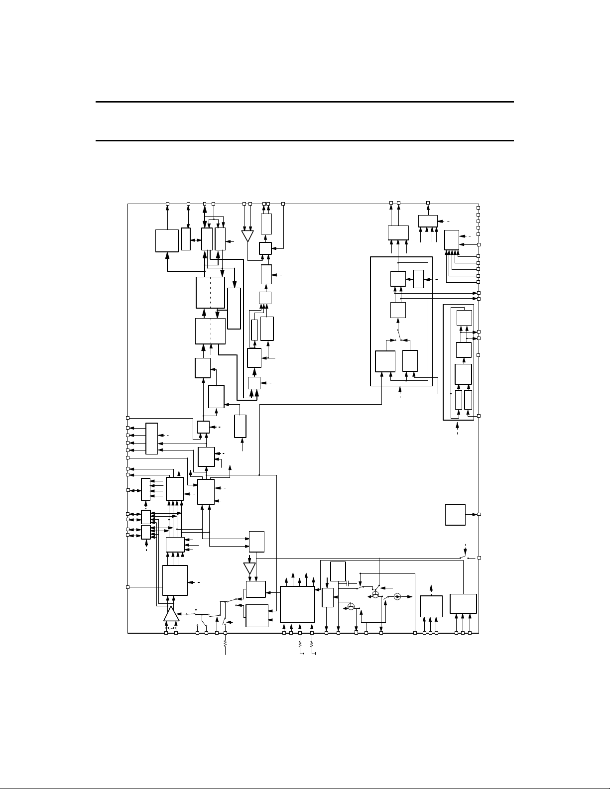
BLOCK DIAGRAM
SM00061
1996 Jul 25 3
Philips Semiconductors P32P4911A
Page 4

Philips Semiconductors Product specification
PRML Read Channel with PR4,
P32P4911A
8/9 ENDEC, FWR Servo
Automatic Gain Control:
• Dual mode AGC, analog during acquisition, sampled during data reads
• Separate AGC level storage pins for data and servo
• Dual rate attack and decay charge pump for rapid AGC recovery (analog)
• Programmable, symmetric, charge pump currents for data reads (sampled)
• Charge pump currents track programmable data rate during data reads (sampled)
• Low drift AGC hold circuitry
• Low-Z circuitry at AGC input provides for rapid external coupling capacitor recovery
• AGC Amplifier squelch during Low-Z
• Wide bandwidth, precision full-wave rectifier
• Programmable AGC controls
– Separate external input pins for AGC hold, fast recovery, and Low-Z control
or
– Internal Low-Z and fast decay timing for rapid transient recovery and AGC acquisition. Timing set with external
resistors (2). Ultra fast decay current set with external resistor. AGC input impedance vs LOWZ = 5:1.
• 2-bit DAC to control AGC voltage in servo mode between 1.1 and 1.4 V
Filter/Equalizer:
• Programmable, 7-pole, continuous time filter provides:
– Channel filter and pulse slimming equalization for equalization to PR4
– Programmable cutoff frequency from 4 to 34 MHz
– Programmable boost /equalization of 0 to 13 dB
– Programmable "zeros" equalization provides time asymmetry compensation
– ±0.5 ns group delay variation from 0.3ƒc to ƒc, with ƒc = 34 MHz
– Minimizes size and power
– Low-Z switch at filter output for fast offset recovery
– No external coupling capacitors required
– DC offset compensation provided at filter output
– Five tap transversal filter for fine equalization to PR4
– Self adapting inner taps (symmetric)
– Programmable outer taps (symmetric, 4-bits)
– Equalization hold input
– "Zeros" channel quality output
– Amplitude asymmetry factor output
Pulse Qualification:
• Sampled Viterbi qualification of signal equalized to PR4
• Register programmable window or hysteresis pulse qualifier for servo reads
• Selectable RDS pulse width and polarity for servo gray code reads
1996 Jul 25 4
Page 5

Philips Semiconductors Product specification
PRML Read Channel with PR4,
8/9 ENDEC, FWR Servo
Time Base Generator:
• Less than 1% frequency resolution
• Up to 141 MHz frequency output
• Independent M and N divide-by registers
• No active external components required
Data Separator:
• Fully integrated data separator includes data synchronizer and 8,9 GCR ENDEC
• Register programmable to 125 Mbit/s operation
• Fast Acquisition, sampled data phase lock loop
• Decision directed clock recovery from data samples
• Adaptive clock recovery thresholds
• Programmable damping ratio for data synchronizer PLL is constant for all data rates
• Data scrambler/descrambler to reduce fixed pattern effects
• 4-bit nibble and byte-wide NRZ data interfaces
• Nibble clock is available during byte-wide mode
• Time base tracking, programmable write precompensation
• Differential PECL write data output
• Integrated sync byte detection, single byte or dual ("or" type)
• Semi-auto training and sync byte generation available for single sync byte operation
• Surface defect scan mode
P32P4911A
Servo:
• Wide bandwidth, precision full-wave rectifier
• Separate, automatically selected, registers for servo ƒc, boost, and threshold
• SEROUT and SREF pins to provide a differential full-wave rectified servo signal
• SELVRC and SDIEN control pins for dc gain and offset calibration
• AGCREF output to provide 2-bit DAC-controlled voltage for applications requiring a fixed gain in servo mode
1996 Jul 25 5
Page 6

Philips Semiconductors Product specification
PRML Read Channel with PR4,
P32P4911A
8/9 ENDEC, FWR Servo
FUNCTIONAL DESCRIPTION
The Philips Semiconductors P32P4911A implements a complete high performance PR4 read channel, including an
AGC, programmable filter/equalizer, adaptive transversal filter, Viterbi pulse qualifier, time base generator, data
separator with 8,9 ENDEC and scrambler/descrambler, and FWR servo, that supports data rates from 42 to 125 Mbit/s.
Data rates from 33 to 100 Mbit/s are supported by changing a single resistor.
A serial port is provided to write control data to the 17 internal program storage registers.
AGC Circuit Description
The automatic gain control (AGC) circuit is used to maintain a constant signal amplitude at the input of the pulse detector
and sampled data processor while the input to the amplifier varies. The circuit consists of an AGC loop that includes an
AGC amplifier, charge pump, programmable continuous time filter, and a precision, wide band, full wave rectifier.
Depending on whether the read is of servo or data type, the specific blocks utilized in the loop are slightly different. Both
loop paths are fully differential to minimize susceptibility to noise. AGC control can be programmably selected between
direct and timed modes.
AGC OPERATION IN SERVO READ MODE
During servo reads the loop consists of the AGC amplifier with a continuous dual rate charge pump, the programmable
continuous time filter, and the full wave rectifier. The gain of the AGC amplifier is controlled by the voltage stored on the
BYPS hold capacitor (C
at DP/DN (internal nodes) to the value programmed by the 2 SAGCLVL bits in the LDS register. These 2 bits allow
adjustment of the filter's normal output voltage from 1.10 to 1.40 Vppd. Attack currents lower the voltage at the BYPS
pin which reduces the amplifier gain. Decay currents raise the voltage at the BYPS pin which increases the amplifier
gain. The sensitivity of the amplifier gain to changes in the BYPS voltage is approximately 38 dB/V. When the voltage
at BYPS is equal to VRC, the gain from the AGC input to DP/DN will be about 24.9 dB. The charge pump is continuously
driven by the instantaneous voltage at DP/DN. When the signal at DP/DN is greater than 100% of the programmed AGC
level, the normal attack current (ICH) of 416.5 µA is used to reduce the amplifier gain. If the signal is greater than 125%
of the programmed level, the fast attack current (I
approach allows the AGC gain to be quickly decreased when it is too high and minimizes distortion when the proper AGC
level has been acquired. The 100% and 125% levels are relative to the selected AGC level in servo mode.
A constant normal decay current (ID) of 24.5 µA acts to increase the amplifier gain when the signal at DP/DN is less than
100% of the programmed AGC level. The large ratio (416.5 µA:24.5µA) of the normal attack and normal decay currents
enables the AGC loop to respond to the peak amplitudes of the incoming read signal rather than the average value. As
a result the AGC loop will not be able to quickly increase its gain if required to do so. A fast recovery mode is provided
to allow the gain to be rapidly increased to reduce recovery time between mode switches. In the fast recovery mode, the
decay current is increased by a factor of 8 to 196 µA (I
1.74 mA (I
It is recommended that the fast recovery mode be asserted when the AGC fields from a sector are being read. Typically,
this will be just after each transition of SG (Servo Gate), after powerup, and after WG/WG is de-asserted. For example,
if C
BYPS
0.5 µs * 196 µA/500 pF = 196 mV, which will allow the gain to increase by 6 dB in that time. If FASTREC is asserted for
0.5 µs in non-servo mode and C
1000 pF = 98 mV, which will allow the gain to increase by 3 dB in that time. It is recommended that LOWZ be asserted
for 0.5µs just prior to any assertion of FASTREC in order to null any internal DC offsets. However, it is possible to assert
both LOWZ and FASTREC simultaneously to reduce sector overhead. This method should be evaluated under the
actual system operating conditions.
The programmable AGC level in servo mode is provided to allow the servo demodulator dynamic range to be adjusted
over a narrow range.
). This has the effect of speeding up the AGC loop between 4 and 8 times.
CHFR
is 500 pF and FASTREC is asserted for 0.5 µs in servo mode, the voltage at BYPS can increase at most by
). The dual rate charge pump drives C
BYPS
) of 3.5 mA is used to reduce the gain very quickly. This dual rate
CHF
DFR
is 1000 pF, then the voltage at BYP can increase at most by 0.5 µs * 196 µA/
BYP
with currents that drive the differential voltage
BYPS
) and the attack current is increased by a factor of 4.18 to
1996 Jul 25 6
Page 7

Philips Semiconductors Product specification
PRML Read Channel with PR4,
P32P4911A
8/9 ENDEC, FWR Servo
AGC OPERATION IN DATA READ MODE
For data reads, the loop described above is used until the data synchronizer is locked to the incoming VCO preamble,
except that the BYP hold capacitor (C
the normal attack current is 416.5 µA, and the fast attack current is 3.5 mA. The fast recovery mode decay current is
196 µA and the fast recovery mode attack current is 1.74 mA. The above mentioned attack and decay currents are not
scaled with the data rate setting. After the data synchronizer PLL is locked (SFC), the AGC loop is switched to include
the AGC amplifier with a sampled charge pump, the programmable continuous time filter, full wave rectifier, and the
sampling 5-tap equalizer to more accurately control the signal amplitude into the Viterbi qualifier. In this sampled AGC
mode, a symmetrical attack and decay charge pump is used. The "1" sample amplitudes are sampled and held and
compared to the ideal "1" value of 500 mV to generate the error current. The maximum charge pump current value can
be programmed from the Sample Loop Control Register to 0, 34, 68, or 102 µA for maximum data rate and will scale
downward with reduced Data Rate Register values.
AGC Control Modes
The AGC control mode is determined by the state of bit 6 (AGCSEL) of the Control Operating Register #1. If this bit is
0, then the direct, external AGC control method is selected, i.e., AGC uses external signals provided to the FASTREC,
LOWZ, and HOLD input pins. If bit 6 is a 1, the timed AGC control method is selected for generating the internal hold,
fast recovery, squelch, and Low-Z signals.
DIRECT AGC CONTROL MODE
For maximum application flexibility, all AGC mode control inputs are to be externally provided. When the LOWZ input is
High, Low-Z mode is activated. In the Low-Z mode, the AGC amplifier input resistance is reduced to allow quick recovery
of the AGC amplifier input AC coupling capacitors. The ratio of Low-Z to Non Low-Z resistance can be selected as either
15:1 or 5:1 by programming the LZTC bit in the Data Boost Register. During Low-Z mode, the time constant of the
internal AC coupling networks at the filter outputs are also reduced by the ratio determined by the LZTC bit. This time
constant is 300 ns in Low-Z and either 5 µs or 1.5 µs when not in Low-Z mode, depending on the state of the LZTC bit.
Low-Z also forces the AGC amplifier gain to be reduced to near 0 V/V. This mode should be activated during and for a
short time after a write operation. It should also be activated for a short time after each transition of the SG input and on
initial power up.
When theHOLD input is Low, the charge pumps are disabled. This de-activates the AGC loop. The AGC amplifier gain
will be held constant at a level set by the voltage at the BYP or BYPS pins. The value of the capacitor placed at these
pins should be selected to give adequate droop performance when in hold mode as well as to insure stability of the AGC
loop when it is active.
The signal provided to the FASTREC input pin determines if the AGC is in fast recovery mode. During the fast recovery
(FASTREC=1), the attack and decay currents are increased to allow faster recovery to the proper AGC level. If faster
recovery than is provided by FASTREC alone is desired, an ultra fast recovery can be effected by connecting a resistor
between the AGCRST pin and the positive supply VPA. If this resistor is present, whenever FASTREC is entered, the
voltage on the BYP or BYPS capacitor will be pulled up. This causes an extremely rapid increase in the AGC amplifier
gain. The ultra fast current will be disabled the first time that the signal at DP/DN reaches the 125% point. The FASTREC
attack and decay currents are used as long as the FASTREC pin is held High.
) is used instead of BYPS and (C
BYP
). The normal decay current is 24.5 µA,
BYPS
TIMED AGC CONTROL MODE
This timed AGC control mode differs from the direct control mode in that the external control inputs LOWZ, FASTREC,
and HOLD, are typically not used, and therefore, must be deasserted. The equivalent signals are generated internal to
the P32P4911A. These internal signals are generated by one-shots that are triggered by various conditions of the
WG/WG, SG, and PDWN inputs. The one-shot timings for the Low-Z and fastrec signals are set by the resistors
connected to the WRDEL and AGCDEL input pins, respectively and analog ground. The time Low-Z period = 0.1 µs *
(R
is set by the resistor connected between the AGCRST input pin and VPA. In the timed mode, the AGC shall use the
C
1996 Jul 25 7
+ 0.5) kΩ and the fast recovery period = 0.1 µs * (R
WRDEL
BYP
and C
for non-servo and servo modes respectively. The nominal and fast attack and decay currents are the
BYPS
+ 0.5) kΩ. The current for the ultra fast decay mode
AGCDEL
Page 8
Philips Semiconductors Product specification
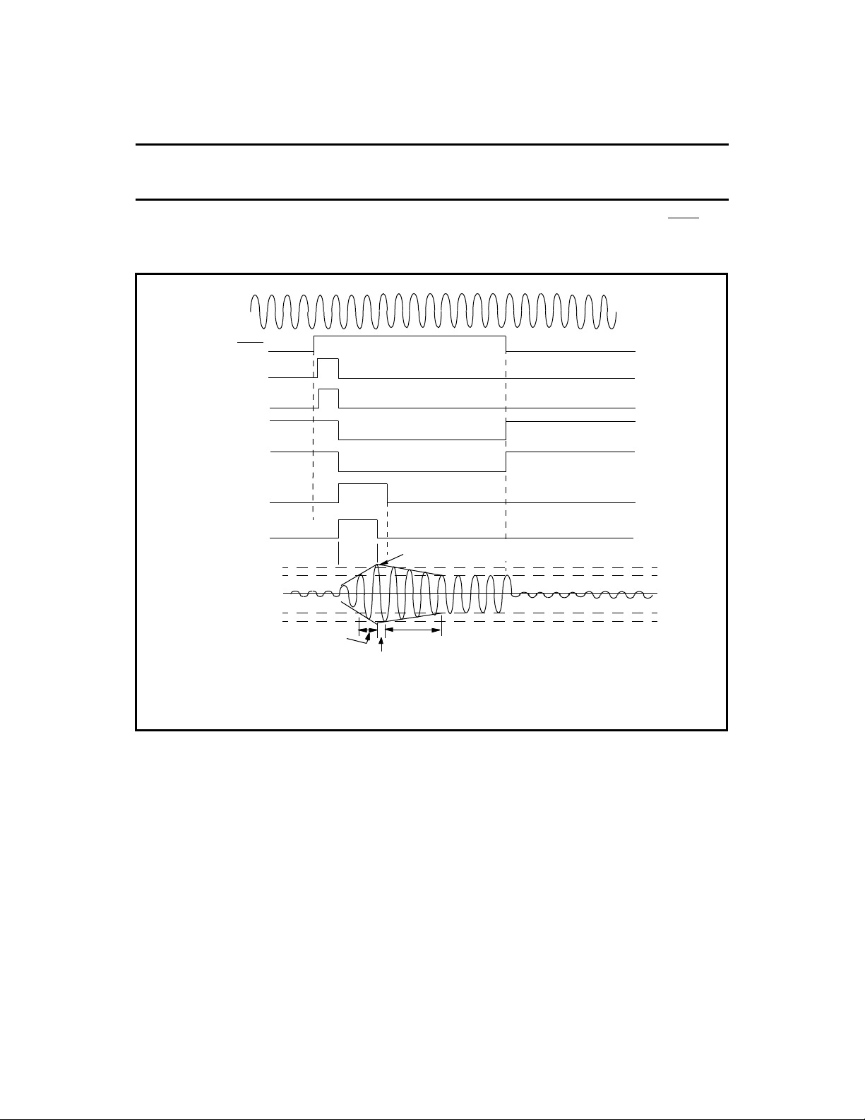
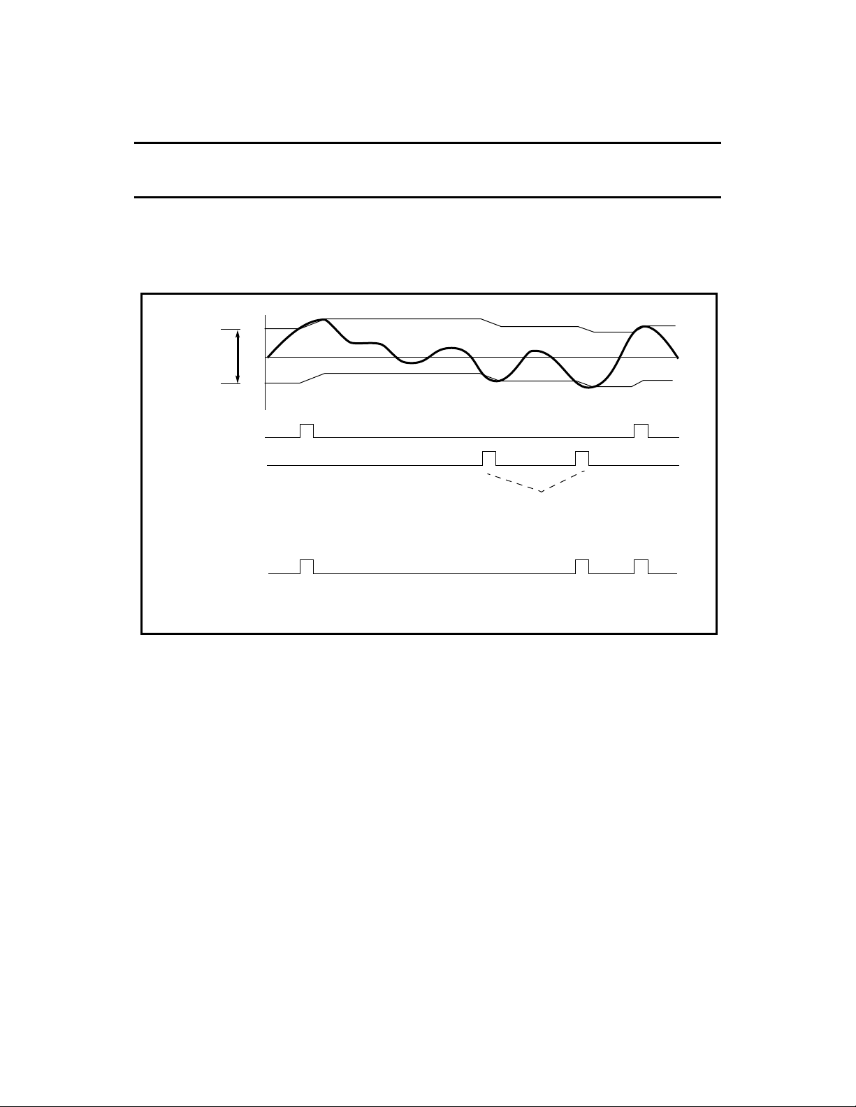
Figure 1: AGC Timing (Internal) Diagrams - Power-On Mode
PDWN
AGC
INPUT
AGC LOWZ
FAST FILTER
OFFSET RECOVERY
AGC HOLD
AGC SQUELCH
AGC FAST RECOVERY
(ATTACK & DECAY)
AGC ULTRA
FAST RECOVERY
(DECAY)
t
LZ
Power-on gain recovery
AGC
OUTPUT
100%
125%
NORMAL
ATTACK
+
-
ULTRA
FAST
DECAY
t
LZ
t
LZ
t
FR
t
LZ
POWERED UP
FAST
ATTACK
Ultra fast decay current is disabled when signal is greater
than 125% of nominal.
PRML Read Channel with PR4,
P32P4911A
8/9 ENDEC, FWR Servo
same in both of the P32P4911A's AGC control modes. In internally timed mode, the LOWZ, FASTREC, and HOLD input
pins are logically OR'ed with their respective internal control signals but do not affect the internal sequencing of the
one-shot generated AGC control signals.
1996 Jul 25 8
Page 9
Philips Semiconductors Product specification
Figure 2: AGC Timing Diagrams - Servo Mode
Servo mode gain recovery
SG
AGC
INPUT
AGC OUTPUT
100%
125%
ULTRA
FAST
DECAY
+
-
AGC LOWZ
FAST FILTER
OFFSET RECOVERY
AGC HOLD
SQUELCH
AGC FAST RECOVERY
(ATTACK & DECAY)
AGC ULTRA
FAST RECOVERY
(DECAY)
t
LZ
t
FR
t
LZ
t
LZ
FAST
ATTACK
t
FR
Ultra fast decay current is disabled when
signal is greater than 125% of nominal.
PRML Read Channel with PR4,
8/9 ENDEC, FWR Servo
P32P4911A
1996 Jul 25 9
Page 10
Philips Semiconductors Product specification
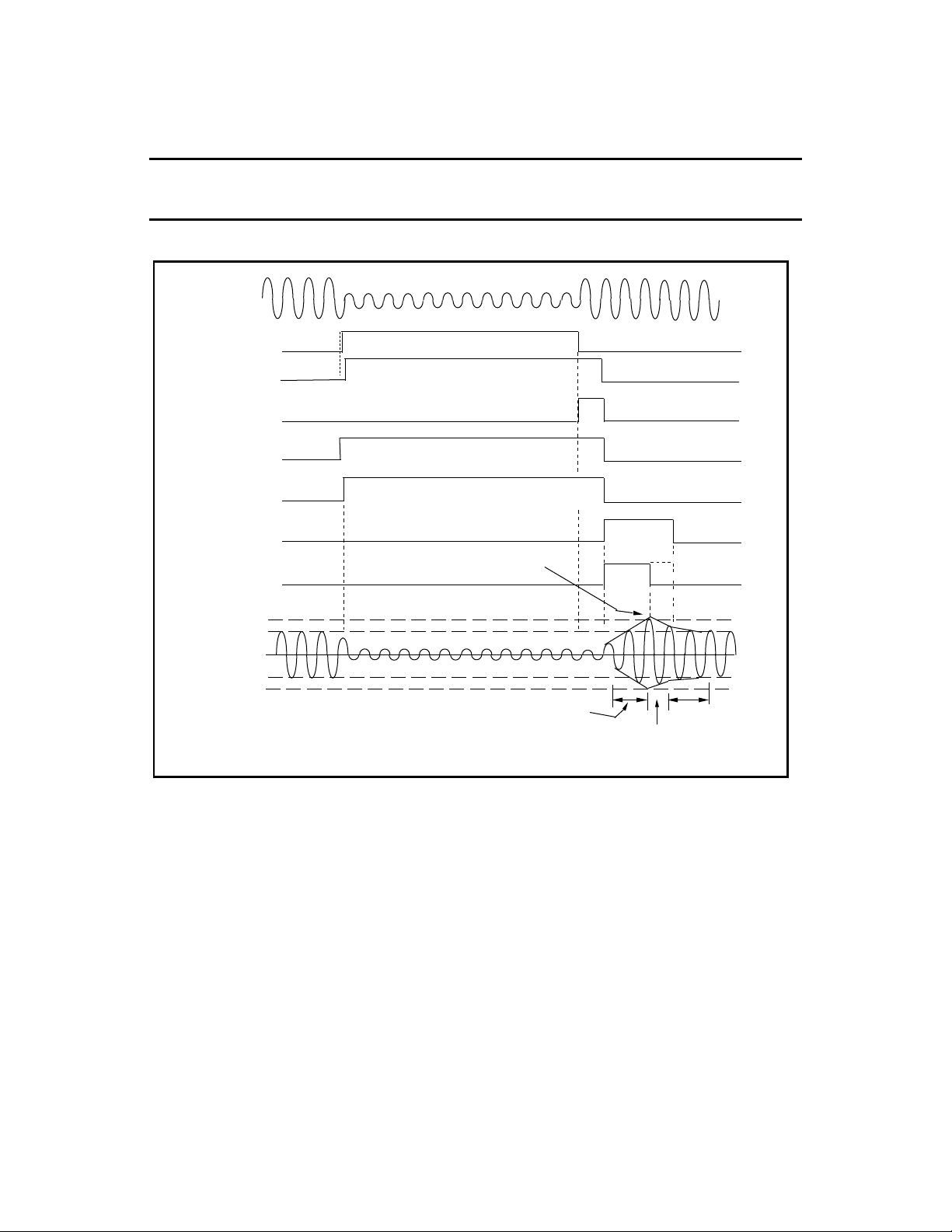
Figure 3: AGC Timing Diagrams - Write Mode
Write mode gain recovery
SG
AGC
INPUT
AGC
OUTPUT
100%
125%
ULTRA
FAST
DECAY
NORMAL
ATTACK
+
-
AGC LOWZ
FAST FILTER
AGC HOLD
AGC SQUELCH
AGC FAST RECOVERY
OFFSET RECOVERY
AGC ULTRA
FAST RECOVERY
t
LZ
t
LZ
(ATTACK & DECAY)
(DECAY)
FAST
ATTACK
t
FR
Ultra fast decay current is disabled when
signal is greater than 125% of nominal.
PRML Read Channel with PR4,
8/9 ENDEC, FWR Servo
P32P4911A
1996 Jul 25 10
Page 11

Philips Semiconductors Product specification
PRML Read Channel with PR4,
P32P4911A
8/9 ENDEC, FWR Servo
Pulse Qualification Circuit Descriptions
This device utilizes three different types of pulse qualification, one exclusively for servo reads, one primarily for servo
reads, and the other for data reads.
SERVO READ MODE
For servo gray code reads, either a dual level (window type) qualifier or a hysteresis type level qualifier may be selected.
If the PDM bit in the Servo Filter Cutoff Register is set to 0, then the window qualifier is selected, and if the PDM bit is a
1, the hysteresis qualifier is selected. The polarity of the RDS/RDS is selected by the SMS bit (Servo Mode Select) in
the Data Rate Register. If SMS=0 then RDS is active-Low and if SMS=1 then RDS is active-High.
DUAL LEVEL (WINDOW) QUALIFIER
During servo reads (SG High) a dual level type of pulse qualifier is used. The level qualification thresholds are set by a
6-bit DAC which is controlled by the Servo Level Threshold Register (LDS). The register value is relative to the peak
voltage at the output of the continuous time filter, derived off of the same reference voltage internal to the chip. The
positive and negative thresholds are equal in magnitude. The state of the adaptive threshold level enable (ALE) bit in
the WP/LT Register does not affect this DAC's reference. The RDS/RDS and the PPOL outputs of the level qualifier
indicate a qualified servo pulse and the polarity of the pulse, respectively. The RDS/RDS and PPOL outputs are only
active when the SG input is High.
HYSTERESIS QUALIFIER
The hysteresis qualifier performs the same as the window qualifier except that the hysteresis qualifier guarantees that
the second of two consecutive pulses of the same polarity will not be qualified. The hysteresis qualifier will only qualify
pulses of alternating polarity.
DATA READ MODE
In data read mode (RG High), the dual level qualifier used for servo reads, is used during VCO sync field counting. Its
qualification thresholds are set by a 6-bit DAC which is controlled by the Data Level Threshold Register (LD). The
register value is relative to the peak voltage at output of the continuous time filter and the DAC both referenced to band
gap voltage. The positive and negative thresholds are equal in magnitude. The state of the adaptive threshold level
enable (ALE) bit in the WP/LT Register does not affect the DAC's reference until the sync field count has been achieved.
The RDS/RDS and the PPOL outputs of the level qualifier are not active in data read mode.
VITERBI QUALIFIER
The second type of pulse qualification, the Viterbi qualifier, is only used during data read mode after the sync field count
has been achieved. The Viterbi qualifier has two significant blocks, one that feeds the other. The first block is the
sampled pulse detector and the second is the survival sequence register.
The sampled pulse detector performs the pulse acquisition/detection in the sampled domain. It acquires pulses by
comparing the code clock sampled analog waveform to the positive and negative thresholds established by the
programmable Viterbi threshold window. The threshold window is defined to be the difference between the positive and
negative threshold levels. The threshold window, Vth, is set by a 7-bit DAC which is controlled by the Viterbi Detector
Threshold Register (VDT). While the window size is fixed by the programmed Vth value, the actual positive and negative
thresholds track the most positive and the most negative samples of the equalized input signal. For example, the Viterbi
positive signal threshold, Vpt = Vpeak (+) max if the previous detected level was (+). If the previous detect level was (-),
Vpt = Vpeak(-)max + Vth, where Vpeak(-)max is the maximum amplitude of the previously detected negative signal.
Normally Vth is set to equal Vpeak (approx. 500 mV).
After the pulses have been detected they must be further qualified by the survival sequence registers and associated
logic. This logic guarantees that for sequential pulses of the same polarity within the maximum run length, only the latest
is qualified. In this way, only the pulse of greatest amplitude will be qualified.
1996 Jul 25 11
Page 12
Philips Semiconductors Product specification
Figure 4: Viterbi Detection
Viterbi
Threshold
WIndow
Viterbi
Detector
Output
+ pulse detect
- pulse detect
For sequential pulses of the same
polarity, the latest is selected by the
survival sequence register logic since
it is always of greater magnitude.
+th
-th
PRML Read Channel with PR4,
P32P4911A
8/9 ENDEC, FWR Servo
The Viterbi qualifier is implemented as two parallel qualifiers that operate on interleaved samples. Each qualifier has a
survival sequence register length of 5.
To facilitate media scan testing, the Viterbi survival sequence register may be bypassed by setting the BYPSR bit in the
Viterbi Detector Threshold (VDT) register.
Programmable Filter Circuit Description
The on-chip, continuous time, low pass filter has register programmable cutoff and boost settings, and provides both
normal and differentiated outputs. It is a 7th order filter that provides a 0.05°phase equiripple response. The group delay
is relatively constant up to twice the cutoff frequency. For pulse slimming two zero programmable boost equalization is
provided with no degradation to the group delay performance. The differentiated output is created by a single-pole,
single-zero differentiator. Both the boost and the filter cutoff frequency for data reads and the filter cutoff frequency for
servo reads are programmed through internal 7-bit DACs, which are accessed via the serial port logic. The nominal
boost range at the cutoff frequency is 0 to 13 dB for data reads and is controlled by the Data Boost Register. In servo
mode, the boost can be programmed in 2 dB steps from 0 to 6 dB by programming the two FBS bits (bits 6 and 7) in the
Filter Boost Servo register. The cutoff frequency, ƒc is variable from 4 to 34 MHz and controlled by the Data Cutoff
Register or Servo Cutoff Register in the servo mode. The cutoff and boost values for servo reads are automatically
switched when servo mode is entered.
The filter zero locations can be programmed asymmetrically about zero to compensate for MR head time asymmetry.
The asymmetry is adjusted by programming the 6 FGD bits (bits 0-5) in the Filter Boost Servo register. The asymmetric
zeros are not usable while in servo mode.
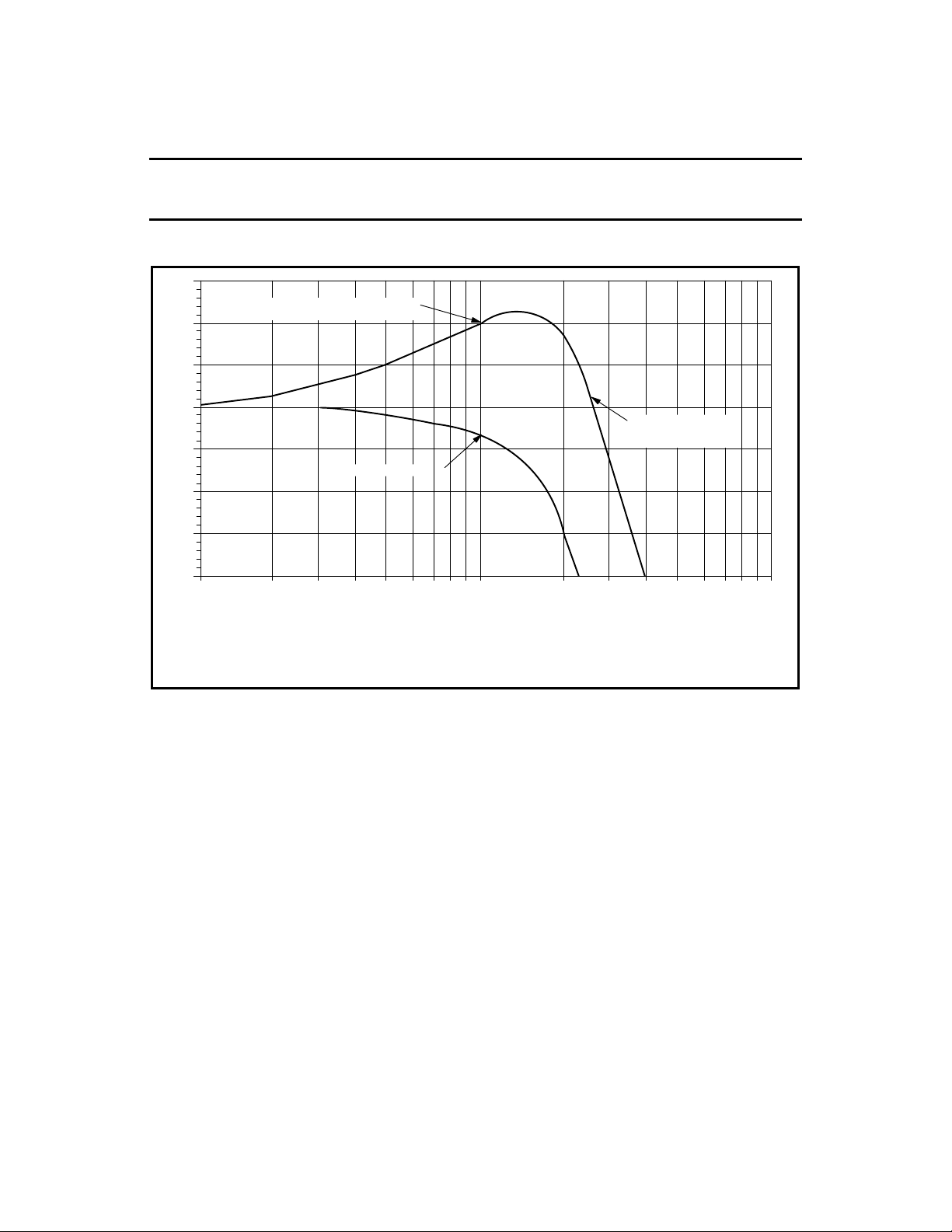
The normal low pass filter is of a seven-pole two-real-zero type. Figure 5 illustrates the transfer function normalized to
1 rad/s. The response can be denormalized to the cutoff frequency of ƒc (Hz) by replacing s by s/2πƒc, while the boost
and group delay equalization are controlled by varying the α and β.
1996 Jul 25 12
Page 13
Philips Semiconductors Product specification
SM00010
IN
s2–s+1.31703
s2+1.68495s+1.31703
2.95139
s
2
+1.54203s+2.95139
5.37034
s
2
+1.14558s+5.37034
0.86133
s+0.86133
s
s+0.86133
Normal
Differential
Figure 5: Programmable Filter Normalized Transfer Function
PRML Read Channel with PR4,
P32P4911A
8/9 ENDEC, FWR Servo
With a zero at the origin, the filter provides a time-differentiated filter output. This is used in time qualification of the peak
detection. To ease the timing requirement in peak detection of a signal slightly above the qualification threshold, the
time-differentiated output is purposely delayed by 1.2 ns relative to the normal low pass output.
The normal low pass output feeds the data qualifier (DP/DN), and the differentiated output feeds the clock comparator
(CP/CN).
Five definitions are introduced for the programmable filter control discussion (Figure 6):
Cutoff Frequency: The cutoff frequency is the -3 dB low pass bandwidth with no boost and group delay equalization, i.e.
α=0 and β=0.
Actual Boost: The amount of peaking in magnitude response at the cutoff frequency due to α≠0 and/or β≠0.
Alpha Boost: The amount of peaking in magnitude response at the cutoff frequency due toα≠0 and without group delay
equalization. In general, the actual boost with group delay equalization is higher than the alpha boost. However, with
>3 dB alpha boost, the difference is minimal. α=1.31703 x (10
Group Delay ∆%: The group delay ∆% is the percentage change in absolute group delay at DC with respect to that
without equalization applied (β=0). β=0.04183 * GD%.
Group Delay Variation: The group delay variation is the change in group delay from DC to the cutoff frequency. This
can be expressed as a percentage defined as: (change in group delay ÷ absolute group delay with β=0) * 100%. An
alternative is to express the group delay variation in nanoseconds. Because the absolute group delay variation in
nanoseconds is scaled by the programmed cutoff frequency, the percentage expression is used in this specification.
BOOST(dB)/20
-1)
1996 Jul 25 13
Page 14
Philips Semiconductors Product specification
Figure 6: Filter Magnitude Response
Frequency (MHz)
Magnitude (dB)
SM00011
15
10
5
0
–5
–10
–15
–20
1 10 100
Cutoff = 10MHz (i) 0dB Alpha Boost & 0% Group Delay Change
(ii) 13dB Alpha Boost & +30% Group Delay Change
–3dB Cutoff Frequency
Actual Boost, same as Alpha Boost with 0%
Group Delay Change or Alpha Boost is large
Actual –3dB Bandwidth
with Boost & Group
Delay Equalization
(i)
(ii)
PRML Read Channel with PR4,
8/9 ENDEC, FWR Servo
P32P4911A
1996 Jul 25 14
Page 15

Philips Semiconductors Product specification
Figure 7: Filter Group Delay Response
70
1 10 100
Cutoff = 0MHz (i) 0dB Alpha Boost & 0% Group Delay Change
(ii) 13dB Alpha Boost & +30% Group Delay Change
DC Group Delay Change
Programmable from
–30% to +30%
(i)
(ii)
1
65
60
55
50
45
40
Group Delay Variation from
‘DC’ to Cutoff Frequency
PRML Read Channel with PR4,
8/9 ENDEC, FWR Servo
Absolute Group Delay (ns)
P32P4911A
Frequency (MHz)
SM00012
FILTER OPERATION
Direct coupled differential signals from the AGC amplifier output are applied to the filter. The programmable bandwidth
and equalization characteristics of the filter are controlled by 3 internal DACs. The registers for these DACs (FC, FB,
and FGD) are programmed through the serial port. The current reference for the DACs is set using a single external
resistor connected from pin VRX to ground. The voltage at pin VRX is proportional to absolute temperature (PTAT),
hence the current for the DACs is a PTAT reference current. This establishes the excellent temperature stability for the
filter characteristics.
The cutoff frequency can be set independently in the servo mode and the data mode. In the data mode, the cutoff
frequency is controlled by the Data Cutoff Register. In the servo mode, the cutoff frequency is controlled by the Servo
Cutoff Register.
CUTOFF CONTROL
The programmable cutoff frequency from 4 to 34 MHz is set by the 7-bit linear FC DAC. The FC register holds the 7-bit
DAC control value. The cutoff frequency is set as:
ƒc (MHz) = 0.301 * FC - 1.142 44 ≤ FC ≤ 117
for servo zones
ƒc (MHz) = 0.277 * FCS + 0.08 14 ≤ FCS ≤ 43
The filter cutoff (ƒc) is defined as the -3 dB bandwidth with no boost applied. When boost/equalization is applied, the
actual -3 dB point will move out. The ratio of the actual -3 dB bandwidth to the programmed cutoff is tabulated in
Table 1 as a function of applied boost and group delay equalization.
1996 Jul 25 15
Page 16

Philips Semiconductors Product specification
PRML Read Channel with PR4,
P32P4911A
8/9 ENDEC, FWR Servo
Table 1: Ratio of Actual -3dB Bandwidth to Cutoff Frequency
Alpha Boost
0 dB 1.62 1.47 1.31 1.16 1.06 1.01 1.00
1 1.74 1.62 1.50 1.38 1.28 1.21 1.19
2 1.87 1.79 1.71 1.63 1.56 1.51 1.49
3 2.01 1.96 1.91 1.87 1.83 1.80 1.79
4 2.14 2.11 2.09 2.07 2.05 2.04 2.03
5 2.25 2.24 2.23 2.22 2.21 2.20 2.20
6 2.35 2.34 2.34 2.33 2.33 2.32 2.32
7 2.44 2.44 2.43 2.43 2.42 2.42 2.42
8 2.52 2.52 2.51 2.51 2.51 2.51 2.51
9 2.59 2.59 2.59 2.59 2.59 2.59 2.59
10 2.67 2.66 2.66 2.66 2.66 2.66 2.66
11 2.73 2.73 2.73 2.73 2.73 2.73 2.73
12 2.80 2.80 2.80 2.80 2.80 2.80 2.80
13 2.87 2.87 2.86 2.86 2.86 2.86 2.86
BOOST CONTROL
The programmable alpha boost from 0 to 13 dB is set by the 7-bit linear FB DAC in data mode or 2-bit linear FBS DAC
in servo mode. The FB register holds the 7-bit DAC control value and the FBS register holds the 2-bit control value. The
alpha boost in data mode is set as:
Alpha Boost (dB) = 20 log [0.021848 * FB + 0.000046 * FC * FB + 1] 0 ≤ FB ≤ 127
The alpha boost in servo mode is set as:
Alpha Boost (dB) = 2 * FBS 0 ≤ FBS ≤ 3
That is, the boost in servo mode can be changed in 2 dB steps from 0 to 6 dB.
The programmed alpha boost is the magnitude gain at the cutoff frequency with no group delay equalization. When finite
group delay equalization is applied, the actual boost is higher than the programmed alpha boost. However, the difference
becomes negligible when the programmed alpha boost is >3 dB. Table 2 tabulates the actual boost as a function of the
applied alpha boost and group delay equalization.
±30% ±25% ±20% ±15% ±10% ±5% ±0%
Group Delay %
1996 Jul 25 16
Page 17

Philips Semiconductors Product specification
PRML Read Channel with PR4,
P32P4911A
8/9 ENDEC, FWR Servo
Table 2: Ratio of Actual -3dB Bandwidth to Cutoff Frequency
Alpha Boost
0 dB 2.81 2.12 1.47 .89 0.42 0.11 0.00
1 3.36 2.76 2.21 1.72 1.33 1.09 1.00
2 3.97 3.45 2.99 2.58 2.27 2.07 2.00
3 4.63 4.19 3.80 3.47 3.21 3.05 3.00
4 5.34 4.97 4.65 4.38 4.17 4.04 4.00
5 6.10 5.79 5.52 5.30 5.14 5.03 5.00
6 6.89 6.64 6.42 6.24 6.11 6.03 6.00
7 7.72 7.51 7.34 7.19 7.09 7.02 7.00
8 8.58 8.41 8.27 8.15 8.07 8.02 8.00
9 9.47 9.33 9.22 9.12 9.05 9.01 9.00
10 10.4 10.3 10.2 10.1 10.1 10.0 10.0
11 11.3 11.2 11.1 11.1 11.0 11.0 11.0
12 12.2 12.2 12.1 12.1 12.0 12.0 12.0
13 13.2 13.1 13.1 13.1 13.0 13.0 13.0
GROUP DELAY EQUALIZATION
The group delay∆% can be programmed between -30% to +30% by the 6-bit linear FGD DAC. The FGD register holds
the 6-bit DAC control value. The group delay ∆% is set as:
Group Delay ∆% = 0.9783 * (FGD4:0) - 0.665 0 ≤ FGD4:0 ≤ 31 and FGD5 = sign bit
The group delay ∆% is defined to be the percentage change of the absolute group delay due to equalization from the
absolute group delay without equalization at DC.
The current reference for the filter DACs is set using a single 12.1 kΩ resistor, from the VRX pin to ground. The voltage
at VRX is proportional-to-absolute-temperature (PTAT).
The outputs of the filter are internally AC coupled to the qualifier inputs and buffers for the filter monitoring test points
TPC+/TPC- and TPD+/TPD-.
±30% ±25% ±20% ±15% ±10% ±5% ±0%
Group Delays ∆%
Internal AC Coupling
The conventional external ac coupling at the filter to qualifier interface has been replaced by a pair of feedback circuits,
one for the normal and one for the differentiated outputs of the filter. The offset of the filter outputs are sensed, integrated,
and fed back to the filter output stage. The feedback loop forces the filter offset nominally to zero. In the normal read
mode, (LOWZ=0), the integration time constant is set to 5 µs until the sync field counter reaches the programmed SFC
count. At the SFC count, the offset sensing is switched into sampled mode and the time constant is reduces to 300 ns.
In sampled mode the offset correction voltage is generated from the zeros qualified by the quantizer. This ensures that
the sampled voltage level, not DP/DN, will be offset free.
1996 Jul 25 17
Page 18

Philips Semiconductors Product specification
PRML Read Channel with PR4,
P32P4911A
8/9 ENDEC, FWR Servo
Amplitude Asymmetry Detection and Correction
In the presence of amplitude asymmetry, such as that generated by MR heads, the sampled data processor (SDP) will
be presented with zeros generated in one of two ways. The first is due the lack of a magnetic transition and will be
referred to as a "real" zero. The second is produced by the superposition of adjacent +1 and -1 magnetic transitions and
results in zero samples that shall be referred to as "cancelled" zeros. In the presence of amplitude asymmetry from an
MR head, the "real" zeros are zero, but the "cancelled" zeros are offset by the difference between the +1 and -1 samples.
The offset correction circuit forces the ground reference of the sampled data processor to the center of the "real" and
"cancelled" zero sample levels.
The integration time constant is increased by a factor of 4 to 1.0 µs, after the sync byte has been detected.
AMPLITUDE ASYMMETRY MONITOR POINT
An amplitude asymmetry quality factor "Qasym" may be selected to be output on the ATO output pin by programming
the ASEL bits in the Power Down Register. This signal is derived by computing the average distance of the "real" and
"canceled" zeros from the sampled data processor's system ground which was established between the two zeros levels
by the offset correction circuit. The average distance is a measure of the asymmetry present in the MR read back signal.
A gain of 4 from the sampled values is utilized and is low pass filtered with a time constant that is programmable to one
of four different values by programming the two QTC bits in the Control Operating Mode Register #2.
The signal is then buffered and differentially multiplexed to the ATO pin. The signal is referenced to MAXREF/2.
The asymmetry quality factor can be held at the value present at sync byte detect by setting the FREZQ bit in the WP/LT
Register. The value will be held for 10 ms and is NOT reset. The ATO output may also be externally filtered to provide
time constants that are appropriate for averaging over major portions of, or an entire sector. The capacitors on externally
added filters must be externally reset. Note that any external filtering added to ATO output pin will affect both the
amplitude asymmetry monitor signal and the equalization quality monitor signal since they are both muxed to the ATO
output pin.
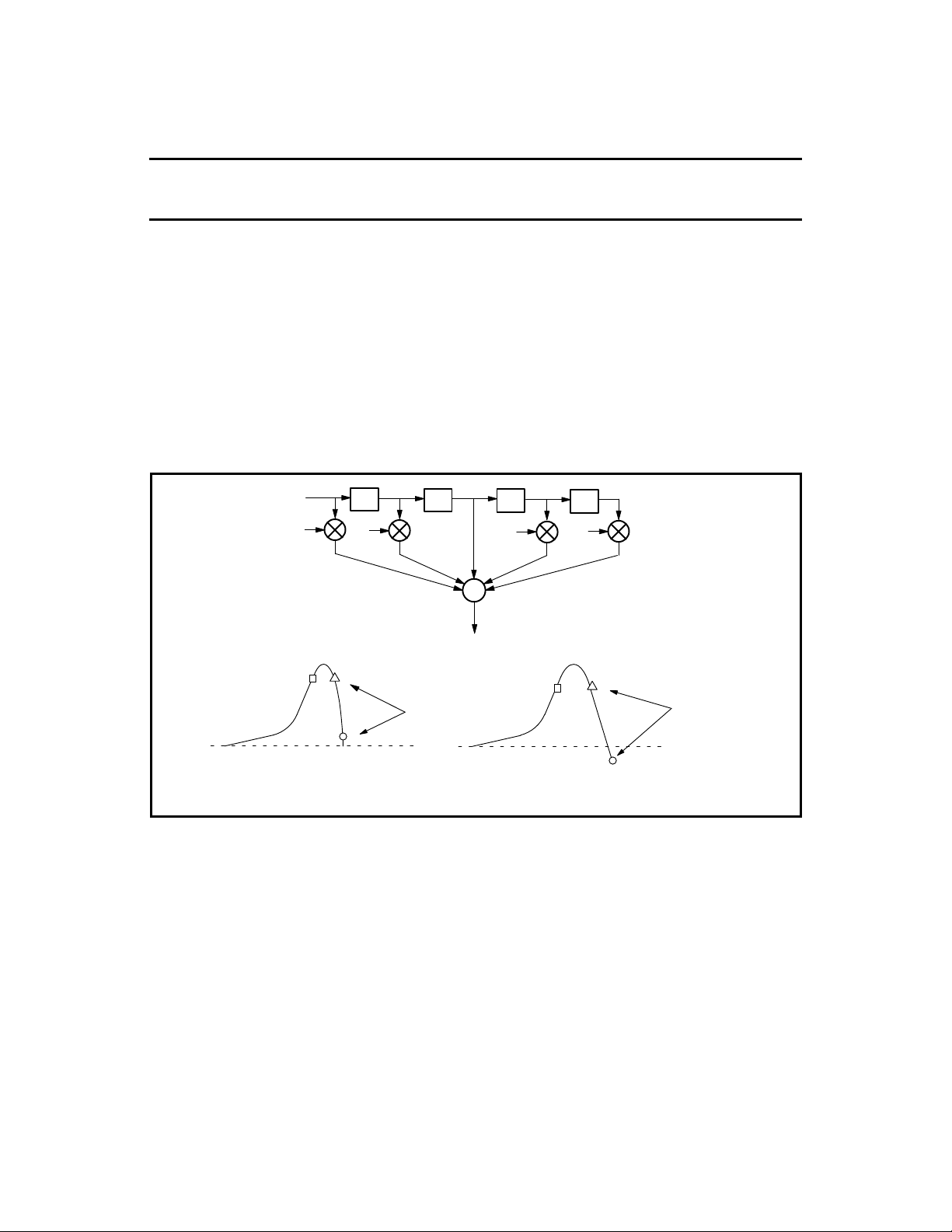
Adaptive Equalizer Circuit Description
Up to 7 dB of equalization for fine shaping of the incoming read signal to the PR4 waveshape is provided by a 5 tap,
sampled analog, transversal filter. This filter provides a self adaptive multiplier coefficient for the inner taps and a
programmable coefficient for the outer taps. Both inner taps use the same coefficient (km1), and both outer taps use the
same coefficient (km2).
For the adaptive inner taps, the value of km1 is adjusted to force "zero" samples to zero volts. A special equalizer training
pattern, located after the VCO sync field in the sector format, is used to provide an optimum signal for the equalizer to
adapt to. The adaptive property of these taps is enabled or disabled by the AEE bit in the Sample Loop Register. If the
adaptive property is enabled, whether adaptation occurs only during the training pattern or both during the training
pattern and the user data is controlled by the AED bit in the Sample Loop Register.
The adaptation can be observed when the equalizer control voltage is selected as the TPA+/TPA- output. The equalizer
control voltage is approximately related to km1 by:
km1 = 0.009 * Date Rate (Mbit/s) * (TPA+ - TPA-)
The multiplier coefficients for the adaptive taps can be held for up to 10 ms if the EQHOLD input is brought High after
sync byte detect has occurred during a previous read in which proper training has occurred. The EQHOLD input pin may
be asserted at any time during a read cycle and the adaptive coefficient Km1 present at that time will be held, provided
no leakage occurs, until the EQHOLD input is de-asserted.
The multiplier coefficient, km2, for the outer taps is programmable between +0.117 and -0.135 by the 4 km bits (bits 4-7)
in the Control Operating Mode Register #2
1996 Jul 25 18
.
Page 19
Philips Semiconductors Product specification
Figure 8: Block Diagram of 5-Tap Equalizer
yn = k
m2
xn + k
m1
x
n-1
+ x
n-2
+ km1 x
n-3
+ km2 x
n-4
need more boost
decrease km
need less boost
increase km
+1
+1
+1
+1
0
0
0V 0V
D
D
D
D
S
x
n
x
n-1
x
n-2
x
n-3
x
n-4
k
m2
k
m1
k
m1
k
m2
y
n
km1 coefficient adapts to force ’0’ samples to 0V
SM00026
PRML Read Channel with PR4,
P32P4911A
8/9 ENDEC, FWR Servo
EQUALIZATION QUALITY MONITOR POINT
An equalization quality factor "Q" may be selected to be output on the ATO output pin by programming the ATOSEL bits
in the Power Down Register and should be used as a guide for selection of the appropriate value for km2. This signal is
derived by computing the absolute distance of the "real" and "canceled" zeros from the sampled data processor's system
ground which was established between the two zeros levels by the offset correction circuit. Then the asymmetry factor
(QASYM) is subtracted and the resulting signal is full wave rectified and low pass filtered using one of the four time
constants that may be programmed with the two QTC bits in the Control Operating Mode Register #2. The signal is then
buffered and differentially multiplexed to the ATO pin. The overall gain to the ATO pin is 4. The signal is referenced to
MAXREF/2.
The equalization quality factor can be held at the value present at sync byte detect by setting the FREZQ bit in the WP/LT
Register. The value will be held for approx. 10 ms and is NOT reset. The ATO output may also be externally filtered to
provide time constants that are appropriate for averaging over major portions of, or an entire sector. The capacitors on
externally added filters must be externally reset.
Time Base Generator Circuit Description
The time base generator (TBG) is a PLL based circuit, that provides a programmable reference frequency to the data
separator for constant density recording applications. This time base generator output frequency can be programmed
with a less than 1% accuracy via the M, N and DR Registers. The TBG output frequency, Fout, should be programmed
as close as possible to ((9/8) * NRZ Data Rate). The time base also supplies the timing reference for write
precompensation so that the precompensation tracks the reference time base period.
The time base generator requires an external passive loop filter to control its PLL locking characteristics. This filter is
fully-differential and balanced in order to reduce the effects of common mode noise.
In read, write and idle modes, the programmable time base generator is used to provide a stable reference frequency for
the data separator. In the write and idle modes, the Time Base Generator output, when selected by the Control Test
Mode Register, can be monitored at the TPB+ and TPB- test pins. In the read mode, the TBG output should not be
selected for output on the test pins so that the possibility of jitter in the data separator PLL is minimized.
1996 Jul 25 19
Page 20

Philips Semiconductors Product specification
Figure 9: Data Synchronizer Phase Locked Loop
A
VCO
CHARGE
PUMP
READ MODE
IDLE/WRITE
MODE
KDS
KDI
Gm
M
Cint
12pF
Cext
KVCO
Sampled Read Data
from Adaptive Equalizer
Reference Frequency
from Time Base Generator
VCO
DS CLK
SAMPLED DATA
PHASE DETECTOR
PHASE/FREQUENCY
DETECTOR
PRML Read Channel with PR4,
P32P4911A
8/9 ENDEC, FWR Servo
The reference frequency is programmed using the M and N registers of the time base generator via the serial port, and
is related to the external reference clock input, FREF, as follows:
F
= FREF * [(M + 1) ÷ (N + 1)]
TBG
The M and N values should be chosen with the consideration of phase detector update rate and the external passive
loop filter design. The Data Rate Register must be set to the correct VCO center frequency. The time base generator
PLL responds to any changes to the M and N registers, only after the DR register is updated.
The DR register value, directly affects the following:
center frequency of the time base generator VCO,
center frequency of the data separator VCO,
phase detector gain of the time base generator phase detector,
phase detector gain of the data separator phase detector,
write precompensation
The reference current for the DR DAC is set by an external resistor, RR, connected between the RR pin and ground.
RR = 10.0 kΩ for 42 to 125 Mbit/s data rate range
RR = 12.1 kΩ for 33 to 100 Mbit/s data rate range
Data Separator Circuit Description
The Data Separator circuit provides complete encoding, decoding, and synchronization for 8,9 (0,4,4) GCR data. In data
read mode, the circuit performs clock recovery, code word synchronization, decoding, sync byte detection, descrambling,
and NRZ interface conversion. In the write mode, the circuit generates the VCO sync field, scrambles and converts the
NRZ data into 8,9 (0,4,4) GCR format, precodes the data, and performs write precompensation.
The circuit consists of five major functional blocks; the data synchronizer, 8,9 ENDEC, NRZ scrambler/descrambler, NRZ
interface, and write precompensation.
DATA SYNCHRONIZER
The data synchronizer uses a fully integrated, fast acquisition, PLL to recover the code rate clock from the incoming read
data. To achieve fast acquisition, the data synchronizer PLL uses two separate phase detectors to drive the loop. A
decision-directed phase detector is used in the read mode and phase-frequency detector is used in the idle, servo, and
write modes.
1996 Jul 25 20
Page 21

Philips Semiconductors Product specification
PRML Read Channel with PR4,
P32P4911A
8/9 ENDEC, FWR Servo
In the read mode the decision-directed timing recovery updates the PLL by comparing amplitudes of adjacent "one"
samples or comparing the "zero" sample magnitude to ground for the entire sample period. A special (non IBM) algorithm
is used to prevent "hang up" during the acquisition phase. The determination of whether a sample is a "one" or a "zero"
is performed by a dedicated, dual mode, threshold comparator. This comparator's threshold levels are determined by
the value, Lth, programmed in the Data Threshold Register. The fixed level threshold before the sync field count (SFC)
has been achieved will be 1.4 times the threshold level after SFC since this is the ratio of the peak signal to the sampled
"1" signal amplitude for PR4. The dual mode nature of this comparator allows the selection of either symmetric fixed or
independent self adapting (+) and (-) thresholds by programming the adaptive level enable (ALE) bit in the WP/LT
Register. Also at SFC, the gain of the phase detector is reduced by a factor of 6 or 10, selectable by the GS bit in the
Damping Ratio Control register. This gain shift increases the loop's noise immunity during data tracking by reducing its
bandwidth.
The adaptive reference allows the specification of the threshold value to be a percentage of an averaged peak value.
When adaptive mode is selected, the fixed thresholds are used until the sync field count (SFC) has been reached, then
the adaptive levels are internally enabled. The time constant of a single pole filter that controls the rate of adaptation, is
programmable by bits TC2-1 in the WP/LT Register.
In the write and idle modes the non-harmonic phase-frequency detector is continuously enabled, thus maintaining both
phase and frequency lock to the time base generator's VCO output signal, F
output current pulses correspond to the direction and magnitude of the phase error.
The two phase detectors' outputs are muxed into a single differential charge pump which drives the loop filter directly.
The loop filter requires an external capacitor. The loop damping ratio is programmed by bits 6-0 in the Damping Ratio
Control Register. The programmed damping ratio is independent of data rate.
In write mode, the TBG output is used to clock the encoder, precoder, and write precompensation circuits. The output
of the precompensation circuit is then fed to the write data flip-flop which generates the write data (WD, WD) outputs.
. The polarity and width of the detector's
TBG
ENDEC
The ENDEC implements an 8,9 (0,4,4) Group Coded Recording (GCR) algorithm. The code has a minimum of no zeros
between ones and a maximum of four zeros between ones for the interleaved samples. During write operations the
encoder portion of the ENDEC converts 8-bit parallel, scrambled or nonscrambled, data to 9-bit parallel code words that
are then converted to serial format. In data read operation, after the code word boundary has been detected in the Viterbi
qualified serial data stream, the data is converted to 9-bit parallel form and the decoder portion of the ENDEC converts
the 9-bit code words to 8-bit NRZ format.
SYNC BYTE DETECTION
The P32P4911A supports two types of sync byte detection, dual byte and single byte.
DUAL SYNC BYTE DETECTION
The P32P4911A implements a dual "or" type sync byte detection scheme to reduce the probability that a single bit error
will lead to the inability to synchronize. The two sync bytes are different and are spaced apart by one byte. The first sync
byte is 1FH and the second is 69H. Sync byte detection is considered to have occurred if either of the two sync bytes is
found but the sync byte detect output pin (SBD) is transitioned at the position in time when the second sync byte (69)
would have been detected. The data placed on the NRZ outputs when SBD goes Low is always the second sync byte
(69) regardless of which of the two was actually detected.
SINGLE SYNC BYTE DETECTION
Since the P32P4911A looks for either of the two sync bytes, the absence of the first sync byte is not an error. This allows
for only a single byte to be written and still be able to achieve synchronization. It is recommended that only the 69H be
written if single sync byte detection is desired so that when detection occurs, the data output on the NRZ pins at sync
byte detect will match the sync byte written.
1996 Jul 25 21
Page 22

Philips Semiconductors Product specification
Figure 10: P32P4911A Scrambler Block Diagram
X0 X1 X2 X3 X4 X5 X6 X7 X8 X9
XOR
NRZ0-7
SCRAM0-7
XOR
PRML Read Channel with PR4,
P32P4911A
8/9 ENDEC, FWR Servo
SINGLE SYNC BYTE DETECTION WHEN SEMI AUTOMATIC TRAINING IS ENABLED
When the AUTOTR bit is set in the Control Operating Register, the training/sync byte sequence is generated with an
internal state machine. The internal state machine generates the 5-byte equalizer training pattern (93H) followed by the
second sync byte (69H); the first sync byte (1FH) is not written by the internal state machine. To initiate the writing of
the training pattern and sync byte in this mode, an FFH must be placed on the NRZ bus for 6 byte times prior to the user
data. This mode may be desirable if controller state machine space is very limited.
SCRAMBLER/DESCRAMBLER
The scrambler/descrambler circuit is provided to reduce fixed pattern effects on the channel's performance. It is enabled
or disabled by bit 2 (SD) of the Control Operating Register. In write mode, if enabled, the circuit scrambles the 8-bit
internal NRZ data before passing it to the encoder. Only user data, i.e., the NRZ data following the second sync byte
(69H), is scrambled. In data read mode, only the decoded NRZ data after the second sync byte (69H) is descrambled.
The scrambler polynomial is H(X)= 1 ⊕ X7 ⊕ X10. The scrambler block diagram is shown in Figure 10. The scrambler
contributes no delay in either the encode or decode paths and therefore there is no difference in path delays whether or
not the scrambler is enabled.
NTERFACE
NRZ I
The NRZ interface circuit provides the ability to interface with either a nibble or byte-wide controller. The NRZ interface
type is specified by the programming of bit 4 (NIB) of the Control Operating Register. If byte-wide mode is selected, the
circuit does not reformat the data before passing it to and from the internal 8-bit bus. If nibble mode is selected, the NRZ
interface circuit converts the 4 LSBs of the external 8-bit bus to the internal 8-bit bus. Only the selected NRZ interface
is enabled and the unused bits can be left floating. Both the byte-wide and nibble interfaces define the most significant
bit of the interface as the most significant bit of the data and the nibble interface defines the first nibble clocked in or out
as the most significant of the pair.
For both byte-wide and nibble operation, the NRZ write data is latched by the P32P4911A on the rising edge of the WCLK
input. The WCLK frequency must be appropriate for the data rate chosen or else overflow/underflow will occur. It is
recommended that WCLK be connected to RCLK to prevent this from occurring. In byte-wide mode, as each NRZ byte
is input to the P32P4911A, its parity is checked against the controller supplied parity bit NRZP.
In data read mode, the NRZ data will be presented to the controller near the falling edge of RCLK so that it can be latched
by the controller on the rising edge of RCLK. When RG goes High, the selected NRZ interface will output Low data until
the sync byte has been detected. The first non-zero data presented will be the sync byte (69H). The NRZ interface is
1996 Jul 25 22
Page 23

Philips Semiconductors Product specification
Figure 11: NRZ Timing
RCLK
NRZ0-7
Read Mode-Byte Wide
byte 0 byte 1
WCLK
NRZ0-7
Write Mode-Byte Wide
byte 0 byte 1
RCLK
Read Mode-Nibble
NRZ1
bit 5
bit 4
bit 0
NRZ0
WCLK
NRZ1
bit 5
bit 4
bit 0
Write Mode-Nibble
bit 4
NRZ0
bit 7
bit 5
bit 3
bit 1
bit 7
NRZ3
bit 6
bit 2 bit 6
NRZ2
NRZ3
bit 7
bit 5
bit 3
bit 1
bit 7
bit 6
bit 4
bit 2 bit 6
NRZ2
byte 0 = MSN byte 0 = LSN byte 1 = MSN
byte 0 = MSN byte 0 = LSN byte 1 = MSN
Figure 12: Precoder Block Diagram
D
XOR
WRITE CURRENT
CODED DATA
D
PRML Read Channel with PR4,
P32P4911A
8/9 ENDEC, FWR Servo
at a high impedance state when not in data read mode. In byte-wide mode, an even parity bit , NRZP, is generated for
each output byte.
W
RITE PRECODER
The P32P4911A implements a 1/(1⊕D2) write precoder which is used to precode the serialized encoder data for PR4.
The state of the precoder is preset to 0,0 upon exiting write mode. This guarantees that precoder will begin the next write
in the 0,0 state. The state of the precoder is not guaranteed when the write data (WD/WD) changes from sync field to
encoded data. The result is that one of 2 different write data patterns or their inverses may be written for a particular
write. All four of these patterns will decode properly upon read back. As a result of the fact that the write data toggle
flip-flop is utilized as part of the precoder, the read/write amplifier connected to the P32P4911A must not contain a T
flip-flop. The precoder block diagram is shown in Figure 12.
1996 Jul 25 23
Page 24

Philips Semiconductors Product specification
Figure 13: RDS/RDS and PPOL vs. DP/DN Relationship
DP/DN
+ Threshold
- Threshold
RDS
PPOL
(+LSth)
(-LSth)
PRML Read Channel with PR4,
P32P4911A
8/9 ENDEC, FWR Servo
WRITE PRECOMPENSATION
The write precompensation circuitry is provided to compensate for media bit shift caused by magnetic nonlinearities. The
circuit recognizes specific write data patterns and can add delays in the time position of write data bits to counteract the
magnetic nonlinearity effect. The magnitude of the time shift, WPC, is programmable via the Write Precomp Register
and is made proportional to the time base generator's VCO period (i.e., data rate). The circuit performs write
precompensation only on the second of two consecutive "ones" and only shifts in the late direction. If more than two
consecutive "ones" are written, all but the first are precompensated in the late direction.
Servo Demodulator Circuit Description
Servo functionality is provided by two separate circuits: the servo full-wave rectifier circuit, and the previously described
dual level pulse qualifier circuit. To support embedded servo applications, P32P4911A provides separate programmable
registers for servo mode filter cutoff frequency, boost, and qualification threshold. The values programmed in these
registers are selected upon entry into servo mode (SG=1). The RDS pulse polarity is programmable via the Servo Mode
Select (SMS) bit in the Data Rate Register. This bit also determines the polarity of the RDS/RDS output. In addition, the
RDS/RDS pulse width is also programmable via the RDSPW bit in the sample Loop Control Register (SLC).
The servo demodulator circuit outputs a full wave rectified version of the signal at DP/DN to the SEROUT pin when SG=1.
The signal is referenced to the SREF output pin which is biased at about 3.1V below VPA. The SEROUT signal has a
gain of 0.6 V/Vppd so that a 1.4V signal at DP/DN will produce a 0.84V peak excursion at SEROUT. When SG=0, the
SEROUT pin outputs either SREF or SREF + 200 mV. The SELVRC input pin selects which DC voltage is output in this
mode. The 200 mV offset can be used to calibrate the gain of the A/D converter which is driven by the SEROUT signal.
Servo Timing Outputs
The dual level qualifier that was previously described is used to generate the RDS/RDS and PPOL timing signals. The
RDS/RDS output pin pulses Low for each positive or negative servo peak that is qualified by the dual level qualifier. The
pulse width of RDS/RDS may be selected as either 15 ns or 27 ns with the RDSPW bit in the Sample Loop Control
Register. The PPOL output pin provides the pulse polarity information for the qualified peaks, where PPOL=1 for a
positive peak and PPOL=0 for a negative peak. To reduce noise propagation, the RDS/RDS and PPOL outputs are only
active in servo mode.
Serial Port Circuit Description
The serial port interface is used to program the P32P4911A's seventeen internal registers. The serial port is enabled for
data transfer when the Serial Data Enable (SDEN) pin is High ("1"). SDEN must be asserted High prior to any
1996 Jul 25 24
Page 25

Philips Semiconductors Product specification
Figure 14: Serial Interface Timing
SDEN
SCLK
SDATA
t
C
t
SENS
t
CKL
t
CKH
tDSt
DH
t
SENH
t
SL
COMPLETE REGISTER STRING ID
R/W
“0”
S0 S1 S2 A0 A3 D0 D7
SM00003
PRML Read Channel with PR4,
P32P4911A
8/9 ENDEC, FWR Servo
transmission and it should remain High until the completion of the transfer. At the end of each transfer SDEN should be
brought Low ("0").
When SDEN is High, the data presented to the Serial Data (SDATA) pin will be latched into the P32P4911A on each
rising edge of the Serial Clock (SCLK). Rising edges of SCLK should only occur when the desired bit of address or data
is being presented on the serial data line. Serial data transmissions must occur in 16-bit packets. If more than 16 rising
edges of SCLK are received during the time that SDEN is High, only the last 16 are considered valid. For all valid
transmissions, the data is latched into the internal register on the falling edge of SDEN.
Each 16-bit transmission consists of a read/write control bit (must always be reset, i.e., R/W = "0" for write only) followed
by 3 device select bits, 4 address bits and eight data bits. The device select and address bits select the internal register
to be written to. The device select, address and data fields are input LSB first, MSB last, where LSB is defined as Bit 0.
The three device select bits select the type of device on the Philips Semiconductors serial bus to be communicated with
and must be set to S0 = 0 or 1 (depending on register to be selected), S1 = 1, and S2 = 0 when communicating with the
P32P4911A. The figure below shows the serial interface timing diagram.
Description of Operating Modes
The fundamental operating modes of the P32P4911A are controlled by the Servo Gate (SG), Read Gate (RG), and Write
Gate (WG/WG) input pins. The exclusive assertion of any these inputs causes the device to enter that mode. If none of
these inputs is asserted, the device is in the idle mode. If more than one of the inputs is asserted, the mode is determined
by the following hierarchy: SG overrides RG which overrides WG/WG. The mode that is overriding takes effect
immediately.
RG and SG are asynchronous inputs and may be initiated or terminated at any position on the disk. WG/WG is also an
asynchronous input, but should not be terminated prior to the last output write data (WD/WD) pulse.
1996 Jul 25 25
Page 26

Philips Semiconductors Product specification
PRML Read Channel with PR4,
P32P4911A
8/9 ENDEC, FWR Servo
Mode Control
WG/WG RG DEVICE MODE DESCRIPTION
0/1 0 Idle Mode DS VCO locked to F
0/1 1 Data Read
Mode
1/0 0 Data Write Mode Write mode preamble insertion and data write. DS VCO locked to F
1/0 1 Read Override RG overrides WG/WG which causes any write in progress to cease and
IDLE MODE OPERATION
If SG, RG, and WG/WG are not active, the P32P4911A is in idle mode. When in idle mode, the Time Base Generator
and the Data Separator PLL are running and the Data Separator PLL is phase-frequency locked to the TBG VCO output.
The AGC, continuous time filter, and pulse qualifiers are active but the outputs of the pulse qualifiers are disabled. The
continuous time filter is using its programmed values for cutoff frequency and boost determined by the data mode
registers. The AGC operation is the same as in the VCO preamble portion of a data read. Servo burst capture is
operational in idle mode but the filter and AGC settings are for data reads and not for servo reads as would be the case
if the device was in servo mode. The RDS/RDS and PPOL outputs are disabled in idle mode.
SERVO MODE OPERATION
If SG is High, the device is in the servo mode. This mode is the same as idle except that the filter cutoff and boost settings
are switched from those programmed for data read mode to those programmed for servo mode, the AGC is switched to
servo mode, and the RDS/RDS and PPOL and outputs are enabled. The assertion of SG causes read mode, write mode,
and the power down register settings for the front end to be overridden.
DS PLL acquisition, adaptive equalizer training, code word boundary
search and detect, decode, sync byte detect, and NRZ data output. DS
VCO switched from F
switched from F
word boundary detect. NRZ7-0 active.
RCLK synchronized to F
Data Read Mode to be entered.
. NRZ7-0 tri-stated.
TBG
to RD after preamble detect. RCLK gen. input
TBG
to DS VCO. RCLK re-synchronized to RD at code
TBG
. WD and WD active. NRZ7-0 = inputs.
TBG
TBG
.
WRITE MODE OPERATION
The P32P4911A supports three different write modes; Normal write mode, direct write mode #1 and direct write mode
#2. The direct write modes require that either the direct write bit, bit 0 of the Control Operating Register, or the DWR pin
be active. All three write modes require that the Data Separator be powered on. The active polarity of write gate can be
selected by programming the WGP bit in the Control Operating Register. The PDWN input should be kept Low until all
registers are properly loaded to prevent an illegal write operation at power up.
NORMAL WRITE MODE
The P32P4911A is in the normal write mode if WG/WG is active, DWR is High, and the direct write bit in the Control
Operating Register is Low. A minimum of one NRZ time period must elapse after RG goes Low before WG/WG can be
set active. The Data Separator PLL is phase-frequency locked to the TBG VCO output in this mode.
In normal write mode, the circuit first autogenerates the VCO sync pattern, then scrambles the incoming NRZ data from
the controller, encodes it into 8,9 GCR formatted data, precodes it, precompensates it, feeds it to a write data toggle
flip-flop, and outputs it to the preamp for storage on the disk. When WG/WG goes inactive, the WD/WD outputs remain
enabled but the active pull down current is reduced by a factor of 7 to reduce power consumption and the write data
flip-flop is reset to guarantee that the WD/WD outputs represent a zero state.
In normal write operation, when the write gate (WG/WG) goes active, the VCO sync field generation begins, which
causes a continuous "2T" pattern at the WD/WD outputs {(1,1,-1,-1,1,1,-1,-1...) in the write current domain}. The NRZ
inputs must be Low and must be held Low for the duration of the VCO sync field generation. The minimum required sync
field is equivalent to 8 byte times.
1996 Jul 25 26
Page 27

Philips Semiconductors Product specification
Figure 15: Hard Sector Write Sequence - Dual Sync
GAP
8 BYTES MIN. 4 BYTES MIN. 1 BYTE
NRZ DATA (WRITE) 00H 93H 69H
USER DATA
WG
1 BYTE
1FH
1 BYTE
93H
VCO SYNC
FIELD
TRAINING
SEQUENCE
SYNC
BYTE#1
TRAIN
BYTE
SYNC
BYTE#2
SCRAMBLED AND ENCODED
USER DATA
PRML Read Channel with PR4,
P32P4911A
8/9 ENDEC, FWR Servo
The P32P4911A also allows the precoder to be preset when the first training byte arrives at the precoder. With Control
Operating Mode Register #2 bit 3 (TME) and bit 0 (PCSDIS) set to 0, the P32P4911A allows presetting of the precoder.
Bit 2 (PCSPOL) of the Control Operating Mode Register #2 allows the precoder to be preset if PFSPOL is set to 1 and
reset if set to 0.
TRAINING AND SYNC BYTE GENERATION
The P32P4911A supports two modes of sync byte detection, single byte and dual "or" byte, and two modes of training
and sync byte generation, manual and semi-automatic. The manual mode is generally recommended because it can be
used for either dual or single sync byte detection and provides more flexibility in altering the number of training bytes to
be written. The semi-automatic mode can only be used to generate an internally fixed number of training bytes and a
single sync byte, but saves controller state machine space.
MANUAL MODE
In the manual mode, the device will continue to autogenerate the sync field pattern until a 93H is latched at the NRZ
interface, and detected. The device encodes the 93H pattern and writes the result as the training pattern.
For the single sync byte detection mode, a recommended minimum of 5 bytes of 93H must be written to the NRZ interface
to write the 5 byte equalizer training pattern. Next, the NRZ data must be changed to 69H for 1 byte time to write the
single sync byte.
For the dual sync byte detection mode, a recommended minimum of 4 bytes of 93H must be written to the NRZ interface
to write the minimum 4 byte equalizer training pattern. The NRZ data must then be changed to 1FH for one byte time to
write the first sync byte. The NRZ data must then be changed to 93H for one byte time to write a training/propagation
byte. Next, the NRZ data must be changed to 69H for one byte time to write the second sync byte.
EMI-AUTOMATIC MODE
S
In the semi-automatic mode, the device will continue to autogenerate the sync field pattern until a FFH is latched at the
NRZ interface, and detected. The device then internally generates the encoded the 93H pattern for 5 byte times and
writes the result as the training pattern. It then internally generates the encoded 69H pattern for 1 byte time to write the
single sync byte. To maintain proper controller synchronization, the FFH should be presented at the NRZ interface for
1996 Jul 25 27
Page 28

Philips Semiconductors Product specification
Figure 16: Hard Sector Semi-Auto Write Mode
GAP
8 BYTES MIN. 5 BYTES 1 BYTE
NRZ DATA (WRITTEN TO 4911A) 00H
FFH FFH
USER DATA
WG
NRZ DATA (WRITTEN BY 4911A)
00H 93H 69H
USER DATA
VCO SYNC
FIELD
TRAINING
SEQUENCE
SYNC
BYTE
SCRAMBLED AND ENCODED
USER DATA
PRML Read Channel with PR4,
P32P4911A
8/9 ENDEC, FWR Servo
a total of 6 byte times. Note that the semi-automatic mode can only be used to write single sync byte format and the
training pattern length is fixed at 5. This mode is useful if controller state machine space is extremely limited.
U
SER DATA
The user data must be presented at the NRZ interface immediately following the last NRZ sync byte written. Finally, after
the last byte of user data has been clocked in, the WG/WG must remain active for a minimum of 16 NRZ bit times in
byte-wide mode to ensure the that the device is flushed of data (The delay is 21 NRZ bit times in nibble mode). WG/WG
can then go inactive. WD/WD stops toggling a maximum of 2 NRZ (RCLK) time periods after WG/WG goes inactive.
DIRECT WRITE MODE #1
In this direct write mode, the NRZ data from the byte-wide interface bypasses the scrambler, the 8,9 encoder and the
precoder, but is precompensated before going to the write data flip-flop and then to the WD/WD output pins. The RCLK
output is changed from 9 VCO clock periods to 8 VCO clock periods with a 3/8 duty cycle. The purpose of routing the
signal to the precomp circuit is to generate a return to zero pulse every time a "1" occurs in the data so that the write data
flip-flop is toggled. WCLK is not required to latch the byte-wide NRZ data into the NRZ interface since the data is latched
by an internal version of RCLK, but the NRZ data must be valid no later than 12 ns after the rising edge of the RCLK
output pin. Direct write mode #1 is selected by setting the DW bit (bit 0) in the Control Operating Register. and is entered
when the WG/WG input is active. This mode is not valid when using the nibble NRZ interface. Note that Direct Write
Mode #2 will override Direct Write Mode #1.
DIRECT WRITE MODE #2
In this direct write mode, the data presented at the DWI/DWI input pins directly toggles the write data flip-flop which drives
the WD/WD output pins. No WCLK is required in this mode, and the WD/WD output is not resynchronized. Direct write
mode #2 is selected by driving the DWR input Low and is entered when the WG/WG input is active. Note that the Direct
Write Mode #2 will override Direct Write Mode #1.
DATA READ MODE OPERATION
Data read mode is initiated by setting the Read Gate (RG) input pin High. This action causes the data synchronizer to
begin acquisition of the clock from the incoming VCO sync pattern. To achieve this, the data synchronizer utilizes a fully
integrated fast acquisition PLL to accurately develop the sample clock. This PLL is normally locked to the time base
1996 Jul 25 28
Page 29

Philips Semiconductors Product specification
Figure 17: Read Sequence - Dual Sync Byte Modes
GAP
8 BYTES MIN. 5 BYTES MIN. 1 BYTE
NRZ DATA
HIGH Z 00H
00H
00H
USER DATA
RG
SBD
1 BYTE
69H
1 BYTE
00H
SYNC
BYTE#2
SYNC
BYTE#1
TRAIN
BYTE
TRAINING
SEQUENCE
VCO SYNC
FIELD
SCRAMBLED AND ENCODED
USER DATA
PRML Read Channel with PR4,
P32P4911A
8/9 ENDEC, FWR Servo
generator output, but when the Read Gate input (RG) goes High, the PLL's reference input is switched to the filtered
incoming read signal.
A
CQUISITION OF DS VCO SYNC
When the Read Gate input is asserted, the read sequence is initiated. At this time an internal counter begins counting
the pulses that are qualified by the dual level pulse qualifier given the polarity changes of the incoming 1,1,-1,-1,1,1 read
back pattern defined by the VCO sync field. When the count reaches 4, the internal read gate is asserted and the DS
PLL input is switched from the TBG's VCO output to the sampled data input. This is also the point at which the DS PLL's
phase detector is switched from the phase-frequency detector to the decision directed phase detector. The counter is
also used to determine whether the selected sync field count, SFC, has been achieved. When the counter reaches the
value specified by SFC, the data synchronizer PLL is assumed to be locked and settled (VCO lock). Also at SFC, the
phase detector gain switch and the AGC mode switch occur. To allow for different preamble lengths, the SFC can be set
to 64, 80, 96 or 128 from the Sample Loop Control Register. These values for the SFC may be thought of as the number
of code clock periods in the sync field, but they actually represent twice the number of incoming polarity changes
required.
VCO LOCK, PD GAIN, AGC MODE SWITCH, AND CODE WORD BOUNDARY DETECTOR ENABLE
At SFC, one of two phase tracking methods will be chosen depending on the Enable Phase Detector Gain Switching
(GS) bit in the Control Operating Mode Register. When the GS bit is High, the phase detector gain is reduced by a factor
of 6 or 10 as dictated by the GS_10 bit after the SFC count is reached. When the GS bit is Low, no phase detector gain
switching takes place.
Also after SFC, the AGC feedback will be switched from the continuous time fullwave rectifier to sampled data feedback.
At SFC, the internal VCO lock signal activates the code word boundary detection circuitry to define the proper decode
boundaries. Also, at count SFC, the RCLK generator source switches from the TBG's VCO output to the DS VCO clock
signal which is phase locked to the incoming read data samples. The DS VCO is assumed locked to the incoming read
samples at this point. At SFC a maximum of 1 RCLK time period may occur for the RCLK transition, however, no short
duration glitches will occur. After the code word detection circuitry finds the proper code word boundary, the RCLK
generator is again resynchronized to guarantee that the RCLK is in sync with the data. The RCLK output will not glitch
and will not toggle during this RCLK generator resynchronization for up to 2 byte times maximum.
Also at the code word boundary detect, the internal 9-bit code words are allowed to pass to the ENDEC for decoding.
This decoding will occur until read gate is deasserted.
1996 Jul 25 29
Page 30

Philips Semiconductors Product specification
PRML Read Channel with PR4,
P32P4911A
8/9 ENDEC, FWR Servo
ADAPTIVE EQUALIZER TRAINING SEQUENCE
TRAINING SEQUENCE FOR SINGLE SYNC BYTE MODE
As was previously discussed, in a single sync byte type write sequence, a minimum of 5 bytes of NRZ 93H and one byte
of 69H must be written between the end of the VCO sync field and the beginning of the user data. The 5 bytes of 93H
are 8,9 encoded and precoded during write mode to produce the adaptive equalizer training pattern. During read mode,
the encoded 93H sequence (100110011 read data sequence) and the encoded 69H are used to adaptively train the inner
two taps of the five tap transversal filter in a zero forcing manner. The error at the filter output is integrated to derive the
tap weight multiplying coefficient, Km1. Both of these inner taps use the same Km1. It is anticipated that the continuous
time filter will be used for coarse equalization and that transversal filter will be used adaptively for fine tuning. This will
reduce Km’s range and accuracy requirements. Since there are encoded user data patterns that will not produce an
equalizer correction error, an equalization hold during data mode can be selected from the Sample Loop Control
Register. If the equalizer is programmed to adapt only during the training sequence, the sync byte detect signal is used
to hold the Km1 value. After the training pattern, if the loop is active during user data, the equalizer loop gain will be
reduced by 7. The loop’s integration time constant is made inversely proportional to the selected data rate.
The Km1 coefficient can be held at the present instantaneous value by asserting the EQHOLD input. If EQHOLD is
asserted, the Km1 value will not be changed by either exiting read mode, subsequent training patterns, or by subsequent
data patterns. When EQHOLD is deasserted, the equalizer will resume its normally programmed functionality. The Km1
value can be held with reasonable accuracy for up to 1 ms to make the number of code periods required for acquisition
data rate independent.
TRAINING SEQUENCE FOR DUAL SYNC BYTE MODE
The adaptive equalizer training used for the dual sync byte detection mode is the same as that used in the single sync
byte mode except that the adaptation occurs over the 4 encoded 93H bytes, sync byte #1 (1FH), another 93H and sync
byte #2 (69H). This occurs because the Sync Byte Detect (SBD) is what disables the adaptation if adaptation is enabled
only during the training sequence. The number of consecutive 93H training bytes may be reduced in dual sync byte
mode because the sync byte #1 has been chosen to have the same training properties as the 93H training byte.
SYNC BYTE DETECT AND NRZ OUTPUT
The P32P4911A implements a dual "OR" type sync byte detection which offers increased sync byte detection capability
while maintaining backward compatibility with the single sync byte format and detection. The two bytes of the dual sync
byte are separated by a training byte to allow for Viterbi error propagation that may be caused by an error in the first sync
byte. The training byte 93H was chosen to provide the adaptive equalizer an ideal training signal.
As the read data is 8,9 decoded, it is compared to one of two internally fixed sync bytes (1FH or 69H). If the 1FH byte
is found, the SBD output will go Low 18 code clocks (2 byte times) later and the 69H byte will be the first non-zero byte
presented at the NRZ interface. If a match of the 69H byte is the first found, the sync byte detect (SBD) pin goes Low
and the NRZ output data that until now was held Low, is changed to 69H. The next byte presented on the NRZ outputs
is the first byte of user data. SBD will remain Low and NRZ data will continue to be presented at the NRZ interface until
the read gate is deasserted at which point SBD goes High and the NRZ outputs go to a high impedance state.
SURFACE DEFECT SCAN MODE
The P32P4911A helps check for media defects using the surface defect scan mode. In order to use this mode the part
must have the byte-wide interface enabled. In write mode, all zeros are presented (written) at the NRZ interface. When
this pattern is to be read back, bit 7 (DSE bit) of the N Counter Register is enabled which enables the surface defect scan
mode. The survival sequence register must also be turned off (BYPSR bit). In this mode,SBD will transition Low at SFC.
The NRZ7 pin is monitored. If no defect occurs, the NRZ7 pin will stay Low. If a defect occurs, the NRZ7 pin will transition
1996 Jul 25 30
Page 31

Philips Semiconductors Product specification
Figure 18: Surface Defect Scan Mode
SFC
RG
SBD
RCLK
NRZ7
DEFECT
SM00002
PRML Read Channel with PR4,
P32P4911A
8/9 ENDEC, FWR Servo
High on the falling edge of RCLK and stay high as long as the defect is present, transition back Low on the next falling
edge of RCLK when the defect is not present.
Power Down Operation
The power management modes of the P32P4911A are determined by the states of the Power Down Register bits and
the PDWN and SG inputs. The individual sections of the chip can be powered down or up using the Power Down
Register. A High level in a Power Down Register bit disables that section of the circuit. The power down information
from the Power Down Register takes effect immediately after the SDEN pin goes Low.
When the PDWN input is Low, the chip goes into full power down mode regardless of the power down register settings
or the state of the SG input.
When PDWN is High, SG will force the AGC, filter, and pulse qualifier circuits (front end) to be active by overriding the
front end register bit. The back end power down register bits, which include the Data Separator and Time Base Generator
are not affected by the SG input.
The serial port is active in all power down modes.
The time to restart from a full power down is dependent on the PLL loop filter and the data rate.
The truth table for the various modes of operation is shown below:
SG, PDWN : 1,1 1,0 0,1 0,0
Front End ON OFF R OFF
Data Separator R OFF R OFF
Time Base Generator R OFF R OFF
Serial Port ON ON ON ON
R = Controlled by register bit.
(Register bit =1 turns circuits OFF,
Register bit = 0 turns circuits ON)
1996 Jul 25 31
Page 32

Philips Semiconductors Product specification
PRML Read Channel with PR4,
P32P4911A
8/9 ENDEC, FWR Servo
REGISTER DESCRIPTIONS
Serial Port Register Definitions
Complete Register ID String A3 A2 A1 A0 S2 S1 S0 R/W
Power Down Register (PD) 0 0 0 0 0 1 0 0 04H
TPC/1-0
Bits 7-6
TPC
/D1-0
Bits 5-4 ATOSEL Output select for ATO test point
Bit 3 ACCPL
Bit 2 TB Time Base Generator power down
Bit 1 DS Data Separator power down
Bit 0 PD AGC, Filter, Pulse Detector, and Servo power down
* Servo calibration mode enabled, strobing must occur for operation.
Data Filter Cutoff Register (FC) 0 0 0 1 0 1 0 0 14H
Bit 7 3TAPEN 3 Tap equalizer enable
Bits 6-0 FC6-0 Filter cutoff frequency setting in non-servo mode
Test point C/D control (TME = 0)
TPC+/TPC- TPD+/TPD- TPE
0X = disabled disabled disabled
1X = DP/DN CP/CN disabled SG = 1
1X = disabled disabled disabled SG = 0
Test Point C/D Control (TME = 1)
TPC+/TPC- TPD+/TPD- TPE(AGCSEL=0) TPE(AGSEL=1)
00* = disabled disabled disabled disabled
01 = DP/DN CP/CN disabled low-z oneshot
Servo calibration enabled
input mode to qualifiers, etc.
10 = DP/DN CP/CN full wave fastrec
rectifier out oneshot
output mode from filter/offset canceller
11 = filter filter full wave ultra fast
bypass bypass rectifier out decay ctrl.
00 = MAXREF/2
01 = DAC output enabled DAC test mode
10 = Amplitude Asymmetry Monitor output (QASYM) selected
11 = Channel Equalization Monitor output (Q) selected
Internal AC coupling enable/disable (TME = 0)
0 = Internal AC coupling, AGC switched to sample mode at
SFC
1 = Internal AC coupling, AGC is always in continuous mode
Internal AC coupling enable/disable (TME = 1)
0 = Internal AC coupling is enabled
1 = Internal AC coupling is disabled
0 = power up
1 = power down;
0 = power up
1 = power down;
0 = power up
1 = power down;
0 = enable 5 tap equalizer (Normal operation)
1 = enable only 3 tap equalizer (4901 mode)
ƒc (MHz) = 0.301 * FC - 1.142 44 < FC < 117
dec
1996 Jul 25 32
Page 33

Philips Semiconductors Product specification
PRML Read Channel with PR4,
P32P4911A
8/9 ENDEC, FWR Servo
Serial Port Register Definitions (Continued)
Complete Register ID String A3 A2 A1 A0 S2 S1 S0 R/W
Servo Filter Cutoff Register
(FCS)
Data Filter Boost Register (FB) 0 0 1 1 0 1 0 0 34H
Servo Filter Boost Register
(FBS) and Group Delay
Equalizer Register
Viterbi Detector Threshold
Register (VDT)
Data Level Threshold Register
(LD)
0 0 1 0 0 1 0 0 24H
Bit 7 PDM
Bits 6-0 FCS6-0 Filter cutoff frequency setting in servo mode
Bit 7 LZTC
Bits 6-0 FB6-0 Filter boost setting in data mode
0 1 0 0 0 1 0 0 44H
Bits 7-6 FBS 1-0
Bits 5-0 FGD5-0
0 1 0 1 0 1 0 0 54H
Bit 7 BYPSR
Bits 6-0 VD6-0
0 1 1 0 0 1 0 0 64H
BIts 7-6
Bits 5-0 LD5-0
Servo Peak Detector Mode
0 = Window Qualifier
1 = Hysteresis Qualifier
ƒc (MHz) = 0.277 * FC + 0.0802 14
Non Low-Z vs. Low-Z time constant
0 = 15:1
1 = 5:1
Boost (dB) = 20 * log[0.021848 * FB + 0.000046 * FB * FC + 1]
0
< FB < 127
Filter boost setting in servo mode
00 = 0 dB
01 = 2 dB
10 = 4 dB
11 = 6 dB
Filter Group Delay ∆ % In all modes
Group Delay ∆ % = 0.9783 * (FGD 4-0) - 0.665,
where FGD5 = 1 is positive, 0 is negative
0 ≤ FGD ≤ 31
Survival Sequence Register Bypass/Write Precode Bypass
0 = bypass disabled (normal operation)
1 = bypass enabled
Viterbi qualification threshold voltage
Vth (mV) = 7.874 * VD
45 ≤ VD ≤ 127
Not used
Data level qualification threshold voltage
if WP/LT Register : ALE = 0 (Fixed levels)
Prior to SFC : Lth (mV) = 10.47 * LD
After SFC : Lth (mV) = 7.44 * LD
16 ≤ LD ≤ 63
if WP/LT Register : ALE = 1 (Adaptive levels)
After SFC : Lth (%) = 1.574 * LD
dec
dec
dec
dec
< FC < 43
dec
1996 Jul 25 33
Page 34

Philips Semiconductors Product specification
PRML Read Channel with PR4,
P32P4911A
8/9 ENDEC, FWR Servo
Serial Port Register Definitions (Continued)
Complete Register ID String A3 A2 A1 A0 S2 S1 S0 R/
Servo Level Threshold
Register (LDS)
0 1 1 1 0 1 0 0 74H
Bits 7-6 SAGC
LVL1-0
Bits 5-0 LDS5-0
Servo mode AGC
level control
00 = 1.40 Vppd
01 = 1.30 Vppd
10 = 1.20 Vppd
11 = 1.10 Vppd
Servo level qualification threshold voltage
LSth (mV) = 10.47 * LDS
VRC-AGCREF output
voltage
128 mV
253 mV
378 mV
503 mV
W
1996 Jul 25 34
Page 35

Philips Semiconductors Product specification
PRML Read Channel with PR4,
P32P4911A
8/9 ENDEC, FWR Servo
Serial Port Register Definitions (Continued)
Complete Register ID String A3 A2 A1 A0 S2 S1 S0 R/W
Control Test Mode Register
(CT)
TP3 TP2 TP1 Function TPA+, TPA- TPB+, TPB-
0 0 0 Test Points Off high impedance high impedance
0 0 1 Survival Out/In SSOUT A, B (sngl) SSIN A+, A- (sngl),
0 1 0 Eq Cont/Phase Det Equalizer Control (diff) Phase Detect Out (diff),
0 1 1 Viterbi Survival In SSIN B+,B- (sngl) SSIN A+, A- (sngl),
1 0 0 Equalizer Outputs Equalizer A (diff) Equalizer B (diff)
1 0 1 EQ out/Survival In Equalizer A (diff) SSIN A+, A- (sngl)
1 1 0 EQ out/Survival Out Equalizer A, B (sngl) SSOUT A, B (sngl)
1 1 1 EQ out/VCO/2 Equalizer A, B (sngl) DS VCO/2 (diff) for RG = 1
Control Test Mode Register
(CT)
1 0 0 0 0 1 0 0 84H
Bit 7 EFR
Bit 6 ECP Factory reserved bit, must be set to 0 in application (enables
Bits 5-3 TP3-1
EQ out/TBG out Equalizer A, B (sngl) TBG out (diff) for RG = 0
1 0 0 0 0 1 0 0 84H
Bit 2 RCK2X/
VRDT
Bit 1 DT
Bit 0 FSB/UT
Sample clock source
0 = sample clock is from the DS VCO, normal operation
1 = sample clock is from the TBG output, a test mode
charge pump)
Multiplexed test point selection
Enable double RCLK drive (TME = X)
0 = RCLK drive at 1x in byte wide mode, 2x in nibble mode
1 = RCLK drive at 2x in both byte wide and nibble mode
Enable VRDT input (TME=1)
0 = Viterbi survival outputs to the data decoder, normal use
1 = Digital input to the data decoder, fixed AGC filter gain =
24dB used in testing only.
Enable TBG pump down
0 = not in pump down test mode
1 = continuous pump down, for test only
Training Termination (TME = 0)
0 = termination training when
1 = terminate training 4 bytes after framing
Enable TBG pump up (TME = 1)
0 = not in pump up test mode
1 = continuous pump up, for test use only
FLTR1+ sources current; FLTR1- sinks current
SBD goes Low
1996 Jul 25 35
Page 36

Philips Semiconductors Product specification
PRML Read Channel with PR4,
P32P4911A
8/9 ENDEC, FWR Servo
Serial Port Register Definitions (Continued)
Complete Register ID String A3 A2 A1 A0 S2 S1 S0 R/W
N Counter Register (N) 1 0 0 1 0 1 0 0 94
Bit 7 DSE Defect Scan Enable
Bits 6-0 N6-0 N Counter
M Counter Register (M) 1 0 1 0 0 1 0 0 A4H
Bits 7-0 M7-0 M Counter
Data Rate Register (DR) 1 0 1 1 0 1 0 0 B4H
Bits 7 SMS Servo Mode Select
Bits 6-0 DR6-0 Fvco (MHz) = 9/8 Data Rate = 1.143 * DR + 4.986 for
0 = normal operation
1 = defect scan mode enabled
2 < N < 127
2 < M < 255
F
= FREF * [(M+1) ÷ (N+1)]
TBG
0 = RDS is active Low (normal operation)
1 = RDS is active High
RR = 10 kΩ
37 < DR < 127
1996 Jul 25 36
Page 37

Philips Semiconductors Product specification
PRML Read Channel with PR4,
P32P4911A
8/9 ENDEC, FWR Servo
Serial Port Register Definitions (Continued)
Complete Register ID String A3 A2 A1 A0 S2 S1 S0 R/W
Write Precomp / Level
Threshold Time Constant
Register (WPLT)
WPC3 WPC2 WPC1 WPC0 Write Precomp Magnitude
0 0 0 0 No precomp
0 0 0 1 2.1% code period shift
0 0 1 0 4.2% code period shift
0 0 1 1 6.3% code period shift
0 1 0 0 8.4% code period shift
0 1 0 1 10.5% code period shift
0 1 1 0 12.6% code period shift
0 1 1 1 14.7% code period shift
1 0 0 0 16.8% code period shift
1 0 1 0 21.0% code period shift
1 0 1 1 23.1% code period shift
1 1 0 0 25.0% code period shift
1 1 0 1 27.3% code period shift
1 1 1 0 29.4% code period shift
1 1 1 1 31.5% code period shift
1 1 0 0 0 1 0 0 C4H
Bits 7-6 TC2-1 Adaptive Level qualification threshold time constant for
TC2
0
0
1
1
Bit 5 ALE Enable adaptive level qualification in Decision Directed
Bit 4 FREZQ Freeze Channel Quality Factor and Asymmetry Factor at
Bits 3-0 WPC3-0 Write Precomp setting
Decision Directed Phase Detector. (Valid After SFC)
TC1
0
1
0
1
Phase Detector
0 = fixed level qualification
1 = adaptive mode
Sync Byte Detect
0 = Update during read
1 = Freeze at SBD
Time Constant
200 ns
400 ns
600 ns
800 ns
1996 Jul 25 37
Page 38

Philips Semiconductors Product specification
PRML Read Channel with PR4,
P32P4911A
8/9 ENDEC, FWR Servo
Serial Port Register Definitions (Continued)
Complete Register ID String A3 A2 A1 A0 S2 S1 S0 R/W
Control Operating Register
(CM1)
1 1 0 1 0 1 0 0 D4H
Bit 7 AUTOTR Enables Semi-Automatic training and sync byte generation
0 = disabled (normal operation)
1 = enabled (single sync byte only)
Bit 6 AGCSEL Selects AGC control mode
0 = Direct mode i.e., external control signals must be
provided
1 = Timed mode i.e., control provided by one shot timing
from SG and WG/WG
Bit 5 WGP Write gate polarity
0 = active High, (normal operation)
1 = active Low
Bit 4 NIB Enable Nibble interface
0 = Nibble interface disabled, i.e., byte-wide interface
enabled
1 = Nibble (NRZ3-0) interface enabled
Bit 3 BT Bypass Time Base Generator
0 = data synchronizer reference frequency is TBG output,
(normal operation)
1 = data synchronizer reference frequency is FREF input
Bit 2 SD Disable Data Scrambler/Descrambler
0 = enabled, (normal operation)
1 = disabled
Bit 1 GS DS Phase Detector gain switching
0 = enabled, (normal operation)
1 = disabled
Bit 0 DW Enable Direct Write From Byte-wide NRZ (Bypasses
scrambler and ENDEC)
0 = disabled; (normal operation)
1 = enabled,
1996 Jul 25 38
Page 39

Philips Semiconductors Product specification
--
PRML Read Channel with PR4,
P32P4911A
8/9 ENDEC, FWR Servo
Serial Port Register Definitions (Continued)
Complete Register ID String A3 A2 A1 A0 S2 S1 S0 R/W
Sample Loop Control
Register (SLC)
Damping Ratio Control
Register (DRC)
1 1 1 0 0 1 0 0 E4H
Bit 7 RDSPW RDS output pulse width
0 = 15 ns
1 = 27 ns
Bits 6-5 SFC1-0 Sync Field Count
SFC1
0
0
1
1
SFC0
0
1
0
1
Sync Field Count (code clocks)
64
80
96
128
Bit 4 AEGS Adaptive Equalizer Loop time constant shift
0 = equalizer loop time constant same in preamble and data
fields
1 = equalizer loop time constant is increased to 7X in the
data field elative to the preamble field, i.e. loop gain is
reduced to 1/7
Bit 3 AED Enable Adaptive Equalizer on Data Field
0 = adaptive equalizer disabled after preamble field
1 = adaptive equalizer in use after preamble field,
if AEE bit = 1
Bit 2 AEE Enable Adaptive Equalizer
0 = adaptive equalizer disabled
1 = adaptive equalizer enabled for use in preamble field,
and after the preamble field if AED bit = 1
Bits 1-0 AGC1-0 AGC charge pump current in Sampled AGC mode
AGC charge/discharge current (µA) = 2.66 * AGC * DR/RR
(kΩ)
37 < DR < 127, e.g., RR = 10 kΩ e.g., for DR = 100 and
AGC=10 =2
charge pump current = 53 µA
dec
1 1 1 1 0 1 0 0 F4H
Bit 7 GS_10 Data separator PLL gain shift factor
0 = 6
1 = 10
Bits 6-0 D6-0 Damping amplifier gain A = D * (0.7 / 127)
Damping Ratio =
A KVCO 0.25××
-------------------------------------------2ω
n
1996 Jul 25 39
Page 40

Philips Semiconductors Product specification
PRML Read Channel with PR4,
P32P4911A
8/9 ENDEC, FWR Servo
Serial Port Register Definitions (Continued)
Complete Register ID String A3 A2 A1 A0 S2 S1 S0 R/W
Control Operating Mode
Register #2 (CM2)
0 0 0 0 0 1 1 0 06H
Bits 7-4 KM3-0 Equalizer outer tap coefficient km2
km2 = 0.0168 * KM (KM is in 2's compliment)
0111 = +0.117
0110 = +0.101
0101 = +0.0840
0100 = +0.0672
0011 = +0.0504
0010 = +0.0336
0001 = +0.0168
0000 = 0
1111 = -0.0168
1110 = -0.0336
1101 = -0.0504
1100 = -0.0672
1011 = -0.0840
1010 = -0.1010
1001 = -0.1170
1000 = -0.1350
Bit 3 TME Test Mode Enable
0 = TPC and TPD active when SG = 1 and bit 7 of Power
Down Control Register is 1
1 = TPC and TPD as set by bits 6 and 7 of the Power Down
Control Register
Bit 2 PCSPOL Precoder Polarity State
0 = Precoder state set to 0
1 = Precoder state set to 1
Bits 1-0 QTC1-0 Qasym and Q Time Constant Control (TME = 1)
Qasym Q
00 = 100 ns 50 ns
01 = 200 ns 100 ns
10 = 400 ns 200 ns
11 = 800 ns 400 ns
Bit 0 PCSDIS Precoder Set Disabled (TME = 0)
0 = Precoder initialization enabled
1 = Precoder initialization disabled
1996 Jul 25 40
Page 41

Philips Semiconductors Product specification
PRML Read Channel with PR4,
P32P4911A
8/9 ENDEC, FWR Servo
PIN DESCRIPTIONS
Power Supply Pins
Pin Name Type Pin Function
VPA - AGC / Filter analog circuit supply
VPF - Time Base Generator PLL ECL plus Write pre-comp supply (connect to analog supply)
VPT - Time Base Generator PLL analog circuit supply
VPP - Data Separator PLL analog circuit supply
VPD - TTL Buffer I/O digital supply
VPC - Internal ECL, CMOS logic digital supply
VPS - Sampled data processor supply
VNA - AGC / Filter analog circuit ground
VNF - Time Base Generator ECL ground (connect to analog ground)
VNT - Time Base Generator PLL analog circuit ground
VNP - Data Separator PLL analog circuit ground
VND - TTL Buffer I/O digital ground
VNC - Internal ECL, CMOS logic digital ground
VNS - Sampled data processor ground
VNRX - AGC/Filter analog ground
Analog Input Pins
Pin Name Type Pin Function
VIA+, VIA- I AGC AMPLIFIER INPUTS: Differential AGC amplifier input pins
Analog Output Pins
Pin Name Type Pin Function
TPA+, TPA- O TEST PINS: Emitter output test points. Various signals are multiplexed to these test
TPB+, TPB- O TEST PINS: Emitter output test points similar to TPA+ and TPA-. The pins are used to
TPC+, TPC- O TEST PINS: Bi-directional test points which provide emitter outputs similar to TPA+ and
TPD+, TPD- O TEST PINS: Bi-directional test points which provide emitter output test points similar to
TPE O TEST PIN: Emitter output test point similar to TPA+. Provides servo FWR out when
points by the T est Point Control Register . The signals include the equalizer control voltage
and output, various timing loop control signals and the Viterbi survival register outputs.
The test points are provided to show how the signal is being processed. Internal "pull
down" resistors to ground are provided. To save power when not in test mode, the control
test register bits 3-5 must be set to "0".
look at the other phase of the interleaved signals.
TPA- and provide differential input capability. The pins are used to look at the normal
outputs of the continuous time filter or the AGC amplifier output. These pins can also be
driven with DP/DN like signals for back end testing.
TPA+ and TPA- and provide differential input capability. The pins are used to look at the
differentiated outputs of the continuous time filter or the AGC amplifier output. These pins
can also be driven with CP/CN like signals for back end testing.
enabled.
1996 Jul 25 41
Page 42

Philips Semiconductors Product specification
PRML Read Channel with PR4,
P32P4911A
8/9 ENDEC, FWR Servo
Analog Output Pins (Continued)
Pin Name Type Pin Function
ATO O ANALOG TEST OUT: This test point output provides a monitor of one of three signals.
SEROUT O SERVO OUTPUT: This signal is a full-wave-rectified version of the differential signal at
SREF O SERVO REFERENCE OUTPUT: Reference voltage for the SEROUT signal. It is set to
MAXREF ATO REFERENCE OUTPUT: +3.2V DC reference voltage which can be used as a
AGCREF AGC REFERENCE OUTPUT: Allows programmable fixed gain operation when connected
Analog Control Pins
Pin Name Type Pin Function
BYP
BYPS
FLTR1+,
FLTR1-
FLTR2+,
FLTR2-
RR
VRX
VRC - AGC REFERENCE VOLTAGE: VRC is derived by a bandgap reference from VPA.
WRDEL
AGCDEL
AGCRST
They are the equalizer quality signal, the amplitude asymmetry signal, and the DAC
outputs. The selected output is determined by the programming of the ATOSEL bits in
the Power Down Register. If the DAC outputs are selected, the last DAC written to by the
serial control register is the DAC monitored. Signal at ATO is referenced to MAXREF/2.
DP/DN. It is referenced to the SREF output voltage. Open emitter output which requires
an external pull down current when SDIEN is high. When SDIEN is low, a 360 µA pull
down current is interally provided.
one Vbe below the VRC voltage. This is an open emitter output which requires an
external pull down current when SDIEN is high. When SDIEN is low, a 360 µA pull down
current is interally provided.
baseline for the ATO test point. Can be used for the reference for an external A/D
converter.
to either or both of the BYPD or BYPS pins.
The data AGC integrating capacitor, C
-
is used when not in servo read mode (SG = 0).
The servo AGC integrating capacitor, C
-
pin is used when in servo read mode (SG = 1).
TBG PLL LOOP FILTER: Differential connection points for the time base generator PLL
-
loop filter components.
DS PLL LOOP FILTER: Differential connection points for the data separator PLL loop
-
filter capacitor.
CURRENT REFERENCE RESISTOR INPUT: An external 1%, 10 kΩ (for max data rate
of 125 Mbit/s) or 12.1 kΩ (for max data rate of 100 Mbit/s) resistor is connected from this
-
pin to ground to establish a precise internal reference current for the data separator and
the time base generator DACs.
FILTER REFERENCE RESISTOR INPUT: An external 1%, 12.1 kΩ resistor is connected
-
from this pin to ground to establish a precise PTAT (proportional to absolute temperature)
reference current for the filter DACs.
LOWZ ONE-SHOT ADJUST: The resistor connected between this pin and GND
-
determines the length of the lowz period. tLZ = (RLZ + 0.5) * 0.1 µs/kΩ.
FAST RECOVERY ONE-SHOT ADJUST: The resistor connected between this pin and
-
GND determines the length of the fast decay period. tFR = (RFR+ 0.5) * 0.1 µs/kΩ.
ULTRA FAST DECAY CURRENT ADJUST: The resistor connected between this pin and
-
VPA determines the ultra fast decay current given by the equation I = (VPA - VBYP)/Rufd.
This pin may be left open if ultra fast decay action is not required.
, is connected between BYP and VPA. This pin
BYP
, is connected between BYPS and VPA. This
BYPS
1996 Jul 25 42
Page 43

Philips Semiconductors Product specification
PRML Read Channel with PR4,
P32P4911A
8/9 ENDEC, FWR Servo
Digital Input Pins
Pin Name Type Pin Function
LOWZ I Low-Z MODE INPUT : TTL compatible CMOS control pin which, when pulled High, the input
FASTREC I FAST RECOVERY: TTL compatible CMOS control pin which, when pulled High, puts the
PDWN I POWER DOWN CONTROL: CMOS compatible power control pin. When set to logic
HOLD I AGC HOLD CONTROL INPUT: TTL compatible CMOS control pin which, when pulled
EQHOLD I EQUALIZER HOLD CONTROL INPUT: TTL compatible control pin which, when pulled
FREF I REFERENCE FREQUENCY INPUT: Reference frequency for the time base generator.
WCLK I WRITE CLOCK: TTL compatible CMOS input that latches in the data at the selected
RG I READ GATE: TTL compatible CMOS input that, when pulled High, selects the PLL
WG/WG I WRITE GATE: TTL compatible CMOS input that, when pulled High, enables the write
SG I SERVO GATE: TTL compatible CMOS input that, when pulled High, enables the servo
VRDT I VITERBI READ DATA: A TTL or ac coupled PECL compatible input to the data separator
DWR I DIRECT WRITE MODE 2 ENABLE: Enables DWI, DWI inputs to the write data flip-flop
impedance is reduced to allow rapid recovery of the input coupling capacitor. When pulled
Low, keeps the AGC amplifier and filter input impedance high. An open pin is a logic High.
AGC charge pump in the fast decay mode. An open pin is a logic High.
Low, the entire chip is in sleep mode with all circuitry, except serial port, shut down. This
pin must be set to logic High in normal operating mode. Selected circuitry can be shut
down by the Power Down Register. The PDWN pin must be either driven to a valid
CMOS High level or externally pulled up since it is not internally pulled up.
Low, holds the AGC amplifier gain constant by turning off the AGC charge pump. The
AGC loop is active when this pin is either at High or open.
High causes the present adaptive equalizer tap weights to be held until the input is set
Low. An open pin is at logic High.
FREF may be driven either by a direct coupled TTL signal or by an ac coupled ECL
signal. When bit 3 (BT) of the Control Operating Register (CM1) is set, FREF replaces
the VCO as the input to the data separator.
NRZ interface on the rising edge. Must be synchronous with the write data NRZ input.
For short cable delays, WCLK may be connected directly to pin RCLK. For long cable
delays, WCLK should be connected to an RCLK return line matched to the NRZ data bus
line delay. An open pin is at logic High.
reference input and initiates the PLL synchronization sequence. A High level selects the
RD input and enables the read mode/address detect sequences. A Low level selects the
time base generator output. An open pin is at logic High.
mode. The active state of WG/WG can be selected by the WGP bit in the control
operating register. An open pin is at logic High.
read mode. An open pin is at logic High.
back end, for testing purposes only. This pin is controlled by the VRDT bit in the Control
Test Register (CT).
when input is Low. TTL compatible CMOS levels. Open pin is at logic High.
1996 Jul 25 43
Page 44

Philips Semiconductors Product specification
PRML Read Channel with PR4,
P32P4911A
8/9 ENDEC, FWR Servo
Digital Input Pins (Continued)
Pin Name Type Pin Function
DWI, DWI I DIRECT WRITE INPUTS: Inputs connect to the toggle input of the write data flip-flop
SELVRC I SERVO REFERENCE SELECT: TTL compatable input. When SG is low, this input
SDIEN I SERVO TEST MODE: TTL compatible input that enables an internal pulldown current at
Digital Bi-directional Pins
Pin Name Type Pin Function
NRZ0-7 I/O BYTE WIDE NRZ DATA PORT: TTL compatible CMOS bi-directional input/output. Input
NRZP I/O NRZ DATA PARITY BIT: Active when in Byte-Wide mode. TTL compatible CMOS
Digital Output Pins
Pin Name Type Pin Function
RCLK O READ REFERENCE CLOCK: A multiplexed clock source used by the controller. When
NCLK O NIBBLE MODE CLOCK: A half byte clock synchronized to RCLK. It runs at twice the
SBD O SYNC BYTE DETECT: Transitions Low upon detection of sync byte. This transition is
WD, WD O WRITE DATA: Write data flip-flop output. The data is automatically re-synchronized
RDS/RDS O SERVO READ DATA: Read Data Pulse output for servo read data. Active Low limited
PPOL O SERVO READ DATA POLARITY: Read Data Pulse polarity output for servo read data.
when DWR is Low. PECL input levels. Can be left open.
determines where SREF (SELVRC=high) or SREF + 200 mV (SELVRC = low) is
presented at SREF output. An open pin is logic high.
the SREF and SEROUT pins. An open pin is logic high.
to the encoder when WG/WG is High. Output from the decoder when RG is High. The 4
LSBs are used in nibble mode. The 4 MSBs can be left open if not used.
bi-directional input / output. Generates even read parity when RG is High, and accepts
even write parity when WG/WG is active. Can be left open if not used.
RG is Low, RCLK is synchronized to the time base generator output, F
High, RCLK remains synchronized to F
synchronized to the data separator VCO. During a mode change, no glitches are
generated and no more than one lost clock pulse will occur. Limited swing CMOS output
levels.
frequency of RCLK. Limited swing CMOS output levels. Signal present in byte-wide mode.
synchronous with the sync byte's placement on the NRZ lines. Once it transitions Low,
SBD remains Low until RG goes Low, at which point it returns High. CMOS output.
(independent of the delay between RCLK and WCLK) to the reference clock F
in Direct Write mode 2. Differential PECL output levels.
swing CMOS output. Output active when SG is High, and High when SG is Low. The
RDS/RDS output becomes active High if the Servo Mode Select bit (SMS) in the Data
Rate Register is set.
Active High limited swing CMOS output. Negative pulse = Low, positive pulse = High.
Output active when SG is High.
until the SFC is reached. At that time, RCLK is
TBG
. When RG goes
TBG
TBG
, except
1996 Jul 25 44
Page 45

Philips Semiconductors Product specification
PRML Read Channel with PR4,
P32P4911A
8/9 ENDEC, FWR Servo
Serial Port Pins
Pin Name Type Pin Function
SCLK I SERIAL DATA CLOCK: Positive edge triggered clock input for the serial data. CMOS
SDATA
SDEN I SERIAL DATA ENABLE: A High level input enables data loading. The data is internally
input levels.
SERIAL DATA: Input pin for serial data; 8 register select bits first, followed by 8 data bits.
I
The register select bits and data bits are entered LSB first, MSB last. CMOS input levels.
parallel latched when this input goes Low. CMOS input levels.
1996 Jul 25 45
Page 46

Philips Semiconductors Product specification
PRML Read Channel with PR4,
P32P4911A
8/9 ENDEC, FWR Servo
ELECTRICAL SPECIFICATIONS
Absolute Maximum Ratings
Operation beyond the maximum ratings may damage the device
Symbol Parameter Rating
Vp Positive 5.0V Supply Voltage -0.5 to 7V
Storage Temperature -65 to 150°C
Solder Vapor Bath 215°C, 90s, 2 times
Junction Operating Temperature +135°C
Output Pins ±10 mA
Analog Pins ±10 mA
Voltage Applied to other Pins -0.3V to Vp+0.3V
Recommended Operating Conditions
Unless otherwise specified, the recommended operating conditions are as follows:
4.5V < POSITIVE SUPPLY VOLTAGE < 5.5V, 0°C < T
flowing into the chip are positive.
Current maximums are currents with the highest absolute value.
Power Supply Current and Power Dissipation
Symbol Parameter Test Conditions Min. Nom. Max. Unit
I
CC
PD Power Dissipation
Supply current (VPn) Outputs and test
Normal Mode
PWR Data Separator Off Power Down Register = 2d 500 mW
PWR Data Separator Off
and TBG Off
PWR Idle through serial port Power Down Register = 7d 125 mW
Sleep Mode PDWN = Low 1 9 mW
point pins open
T
= 27°C
amb
Outputs and test
point pins open,
T
= 27°C
amb
Power Down Register = 6d 500 mW
< 55°C for 100-lead LQFP and 25°C < Tj < 135°C. Currents
amb
190 mA
1000 1530 mW
1996 Jul 25 46
Page 47

Philips Semiconductors Product specification
PRML Read Channel with PR4,
P32P4911A
8/9 ENDEC, FWR Servo
Analog Inputs
TEST POINT INPUTS
Symbol Parameter Test Conditions Min. Nom. Max. Unit
TPC±, TPD±
Input Bias Voltage
Digital Inputs
TTL COMPATIBLE CMOS INPUTS
Symbol Parameter Test Conditions Min. Nom. Max. Unit
V
IL
V
IH
I
IL
I
IH
Input Low voltage -0.3 0.8 V
Input High voltage 2.0 VPD+0.3 V
Input Low current VIL = 0.4V -250 µA
Input High current VIH = 2.4V 100 µA
FREF AND VRDT INPUTS
Symbol Parameter Test Conditions Min. Nom. Max. Unit
V
V
I
I
IL
IH
ILF
IHF
Input Low voltage -0.3 0.8 V
Input High voltage 2.0 VPD+0.3 V
Input Low Current VIL = 0.4V -400 µA
Input High Current VIH = 2.4V 500 µA
TPC±,TPD± selected as
inputs
VPA -1.5 V
CMOS INPUTS
Symbol Parameter Test Conditions Min. Nom. Max. Unit
V
ILC
V
IHC
Input Low Voltage VPC = 5.0V 1.5 V
Input High Voltage VPC = 5.0V 3.5 V
PSEUDO ECL COMPATIBLE INPUTS
Symbol Parameter Test Conditions Min. Nom. Max. Unit
V
IL
V
IH
Input Low Voltage VPD-2.0 VIH-0.25 V
Input High Voltage VPD-1.1 VPD-0.4 V
Input Current -100 +100 µA
Digital Outputs
CMOS Outputs
Symbol Parameter Test Conditions Min. Nom. Max. Unit
V
V
OLC
OHC
Output Low voltage IOL = +2 mA 0.45 V
Output High voltage IOH = -100 µA 0.7 * VPD V
1996 Jul 25 47
Page 48

Philips Semiconductors Product specification
PRML Read Channel with PR4,
P32P4911A
8/9 ENDEC, FWR Servo
DIGITAL DIFFERENTIAL OUTPUTS (WD, WD)
Symbol Parameter Test Conditions Min. Nom. Max. Unit
V
OLD
V
OHD
TEST POINT OUTPUT LEVELS
Symbol Parameter Test Conditions Min. Nom. Max. Unit
Output Low Voltage IOL = 2 mA VPD-2.1 V
OHD
-0.3 V
Output High Voltage IOH = 2 mA VPD-1.4 VPD-0.5 V
Output Sink Current -3.5 mA
Differential Voltage | V(WD) - V(WD) | 0.6 Vppd
Test Point Output Swing
0.7 Vppd
TPA+, TPA TPB+, TPB-
TPC+, TPC TPD+,TPD-
C
= 5 pF 1.0 VPA-1.5 V
LOAD
TPE
Source Impedance
30 Ω
TPC+/TPC TPD+/TPD TPE
Output Current
-0.8 +3 mA
TPC+/TPC TPD+/TPD TPE
Common Voltage
2.5 V
TPC+/TPC TPD+/TPD TPE
Serial Port Timing
Refer to Figure 16.
Symbol Parameter Test Conditions Min. Nom. Max. Unit
t
C
t
CKL
t
CKH
t
SENS
t
SENH
t
DS
t
DH
t
SL
SCLK Data Clock Period, 80 ns
SCLK Low time SCLK < 0.8V 30 ns
SCLK High time SCLK > 2.0V 30 ns
Enable to SCLK 40 ns
SCLK to disable 40 ns
Data set-up time 15 ns
Data hold time 15 ns
SDEN min. Low time 160 ns
1996 Jul 25 48
Page 49

Philips Semiconductors Product specification
PRML Read Channel with PR4,
P32P4911A
8/9 ENDEC, FWR Servo
AGC Characteristics
Unless otherwise specified, recommended operating conditions apply.
AGC A
MPLIFIER
The input signals are AC coupled to VIA+ and VIA-. Integrating capacitor C
and VPA. Integrating capacitor C
the output is measured differentially at TPC+ and TPC-, Fin = 5 MHz, the filter frequency ƒc = max
and the filter boost = 0 dB. All specifications apply equally to servo and read mode prior to SFC.
Symbol Parameter Test Conditions Min. Nom. Max. Unit
Input range Filter Boost =0 dB @ ƒc
Input range Filter Boost =11 dB @ ƒc
ON ON± voltage
DP/DN Voltage variation 20mVppd < VIA < 250mVppd 5.0 %
R
in
V
OO
e
in
CMRR Common mode rejection Fixed Gain = 24 dB, Rs = 0 Ω 40 dB
PSRR Power supply rejection Fixed Gain = 24 dB, Rs = 0 Ω 45 dB
measured @ TPC±
Gain range 3 64 V/V
Gain sensitivity BYP or BYPS voltage
Differential input
resistance
Single-ended input
resistance
Output offset change From gain = 3 V/V to 64 V/V
Input noise voltage Fixed Gain = 24 dB, Rs = 0 Ω 15 30 nV/√Hz
= 1000 pF, is connected between BYPS and VPA. Unless otherwise specified,
BYPS
4 MHz ≤ ƒc ≤ 34 MHz, Fin = ƒc
9 MHz ≤ ƒc ≤ 34 MHz, Fin = ƒc
VIA = 20 to 250 mVppd
1,1,-1,-1,--- pattern
DP/DN output selected
5 MHz <ƒc < 34 MHz, Fin = ƒc
Boost = 0 to 13 dB
change
LOWZ = Low, LZTC = Low
LOWZ = Low, LZTC = High
LOWZ = High, LZTC = x
LOWZ = Low, LZTC = Low
LOWZ = Low, LZTC = High
LOWZ = High, LZTC = x
With DC cancellation off
= 1000 pF, is connected between BYP
BYP
20 250 mVppd
20 200 mVppd
1.19 1.40 1.61 Vppd
38 dB/V
5.9
1.7
450
7.6
2.7
634
3.8
1.4
317
8.9
4.0
850
200 mV
kΩ
kΩ
Ω
kΩ
kΩ
Ω
1996 Jul 25 49
Page 50

Philips Semiconductors Product specification
PRML Read Channel with PR4,
P32P4911A
8/9 ENDEC, FWR Servo
AGC Control Section
The input signals are DC coupled into TPC± with TPC± selected as inputs.
Symbol Parameter Test Conditions Min. Nom. Max. Unit
TPC+/
TPC-,
TPD+/
TPD-
I
D
I
DFR
I
CH
I
CHF
I
CHFR
BYP Pin Leakage Current HOLD = Low, V
BYPS Pin Leakage Current HOLD = Low, V
VRC Reference Voltage -100 µA ≤ Io ≤ +500 µA VPA - 2.56 VPA - 2.1 V
Common Mode Input
For test only VPA-1.5 V
Voltage
Decay current
Normal
FASTREC = Low, SG = Low
DR = Data Rate Register
37 < DR < 127
Servo Mode Decay current
Normal
FASTREC = Low, SG = High
TPC+ = TPC-
Fast Decay Current FASTREC = High
TPC+ = TPC-
Normal Attack Current |TPC+ - TPC-| = 0.7875V
FASTREC = Low
Fast Attack Current |TPC+ - TPC-| ≥ 1.09V
FASTREC = Low
Fast Recovery Attack
Current
Sample Data AGC
Peak Charge and
Discharge Currents
|TPC+ - TPC-| = 0.7875V
FASTREC = High
0 ≤ AGC ≤ 3
AGC = AGC1-0
DR = data rate register
37 < DR <127, RR(kΩ)
= VRC -70 +50 nA
BYP
= VRC -70 +50 nA
BYPS
-24.5 µA
-24.5 µA
8 * I
D
-17 * I
-143 * I
-64 * I
+/-2.66
-6
* 10
D
D
D
A
A
A
A
A
* AGC
* DR/RR
Pulse Qualifier Characteristics
Unless otherwise specified, a 100 mVpp sine wave at 15 MHz is AC coupled into VIA±. FC = 127, and FB = 0.
DUAL LEVEL QUALIFIER
See above for input conditions unless otherwise specified.
Symbol Parameter Test Conditions Min. Nom. Max. Unit
L
th
Data Level Threshold Prior to SFC
Lth (mV) = 10.47 * LD
L
th
-11%
L
th
L
th
+11%
V
16 ≤ LD ≤ 63
After SFC
ALE = 0
L
th
-11%
L
th
L
th
+11%
V
Lth (mV) = 7.44 * LD
ALE = 1
Lth (mV) = 1.574 * LD
16 ≤ LS ≤ 63
LS
Servo Level Threshold LSth (mV) = 10.47 * LS
th
RDS/RDS pulse width High
voltage
16 ≤ LS ≤ 63
RDSPW = 0 7.7 15 20 ns
RDSPW = 1 16.8 27 35 ns
LS
th
-11%
LS
th
LS
th
+11%
V
1996 Jul 25 50
Page 51

Philips Semiconductors Product specification
PRML Read Channel with PR4,
P32P4911A
8/9 ENDEC, FWR Servo
DUAL LEVEL QUALIFIER (Continued)
Symbol Parameter Test Conditions Min. Nom. Max. Unit
PPOL to RDS/RDS delay
time
PPOL, RDS/RDS Rise time 15 pF load, 0.8 to 2.4V 8 ns
PPOL, RDS/RDS Fall time 15 pF load, 2.4 to 0.8V 6 ns
Pulse pairing Window and Hysteresis
VITERBI QUALIFIER
See General for input conditions unless otherwise specified.
Symbol Parameter Test Conditions Min. Nom. Max. Unit
V
th
EQUALIZATION QUALITY FACTOR
Unless otherwise specified, measured at ATO pin loaded with 5 pF. VIA± input signal has no asymmetry. Measured
after training sequences. Continuous Training pattern with zeros displaced by ±10% of one's magnitude of 500 mV
Symbol Parameter Test Conditions Min. Nom. Max. Unit
Viterbi threshold voltage Vth (mV) = 7.874 * VD
Reference Voltage No pulse asymmetry
Gain Absolute deviation of zeros
Drift 0.2 mV/µs
PPOL Edge to RDS/RDS
rise/fall, measured at 1.5V
crossing
LSth = 50%. Measured at
the rising/falling edge of
RDS/RDS
Fin = 5 MHz, FCS = 30
45 ≤ VD ≤ 127
ATOSEL1-0 = 00
is multiplied by gain
2.5 12 ns
-2.5 +2.5 ns
Vth - 11% V
Typ.-130mV MAXREF/2 Typ.+130mV V
th
600 mV
Vth+11% V
AMPLITUDE ASYMMETRY QUALITY FACTOR
Unless otherwise specified, measured at ATO pin loaded with 5 pF. VIA± input signal has 10% amplitude asymmetry.
Asymmetry (%) = ((V+1-V-1)/(V+1+V-1)) * 100, where V+1 = positive "1" sample value and V-1= negative "1" sample value.
This is measured with continuous training bytes, 93H, with distance between canceled and non-canceled zeros at 10 %
of one's magnitude of 500 mV or 100 mV.
Symbol Parameter Test Conditions Min. Nom. Max. Unit
Reference Voltage ATOSEL1-0 = 00 Typ.-100mV MAXREF/2 Typ.+100mV V
Qasym at ATO 400 mV
1996 Jul 25 51
Page 52

Philips Semiconductors Product specification
–
0×
PRML Read Channel with PR4,
P32P4911A
8/9 ENDEC, FWR Servo
INTERNAL AC COUPLER CHARACTERISTICS
Unless otherwise specified, Measured at TPC+/TPC- and TPD+/TPD- pins loaded with 5 pF.
Symbol Parameter Test Conditions Min. Nom. Max. Unit
Offset voltage ACCPL = 0 -35 +35 mV
LOWZ Time Constant LOWZ = 1, LZCTR = X 0.3 µs
Non LOWZ Time Constant LOWZ = 0, LZCTR = 0 5 µs
LOWZ = 0, LZCTR = 1 1.5 µs
ATO Buffer Characteristics
Unless otherwise specified, measured at ATO pin loaded with 5 pF. VIA± input signal has no asymmetry.
Symbol Parameter Test Conditions Min. Nom. Max. Unit
Reference voltage ATOSEL 1-0 = 00 Typ. - 100
Swing From Reference Voltage -0.6 +0.6 V
Source Impedance 50 Ω
Drive Capability +/- refers to source/sink +2/-2 +5/-3 mA
Programmable Filter Characteristics
Unless otherwise specified, recommended operating conditions apply. The input signals are AC coupled to VIA+ and
VIA-. All specifications identical for identical data and servo register settings.
Data uses C
from BYP to VPA and servo uses C
BYP
from BYPS to VPA.
BYPS
Symbol Parameter Test Condition Min. Nom. Max. Unit
ƒcr Filter cutoff range ƒc (MHz) = 0.301 * FC - 1.142
44 ≤ FC ≤ 117
ƒc (MHz) = 0.277 * FCS - 0.08
14 ≤ FC ≤ 43
0 dB Boost
ƒca Filter ƒc Accuracy 44 ≤ FC ≤ 117
14 ≤ FC ≤ 43
OD gain to ON gain
mismatch
ƒin = 0.67 * ƒc
0 dB Boost
Mismatch =
ODgain ONgain
--------------------------------------------------ONgain
%
10
Boost @ Fc Boost (dB) = 20 * log [0.021848 *
FB + 0.000046 * FB * FC +1]
Boost accuracy Boost = 13 dB -2.0 +2.0 dB
Boost = 9 dB -1.7 +1.7 dB
Filter Output Dynamic
Range ON±
THD = 2.5%,
ƒin = 0.67 * ƒc, CL = 15 pF
MAXREF/2
Typ. +100 V
4-34 MHz
-15
-20
+15
+20
%
-30 +30 %
0 13 dB
1.4 Vpp
1996 Jul 25 52
Page 53

Philips Semiconductors Product specification
PRML Read Channel with PR4,
P32P4911A
8/9 ENDEC, FWR Servo
Programmable Filter Characteristics (Continued)
Symbol Parameter Test Condition Min. Nom. Max. Unit
TGD Variation ƒc = 34 MHz
Group delay equalization
accuracy
ON+ - ON- output
noise voltage,
no boost
ON+ - ON- output
noise voltage,
max. boost
VRX Rx pin voltage T
Rx resistance 1% fixed value 10.0 kΩ
Fin = 0.3ƒc to ƒc
0 ≤ FB ≤ 127
ƒc = 12 MHz to 34 MHz
Fin =0.3 ƒc to ƒc
0 ≤ FB ≤ 127
ƒc = 4 MHz to 12 MHz
Fin = 0.2ƒc to ƒc
0 ≤ FB ≤ 127
ƒc = 12 MHz to 34 MHz
Fin = ƒc to 1.75ƒc
0 ≤ FB ≤ 127
ƒc = 4 MHz to 12 MHz
Fin = ƒc to 1.75ƒc
0 ≤ FB ≤ 127
Fc = 12-34 MHz, FB = 0 db
% GD = (0.9783 * FGB) - 0.665
BW=100 MHz, Rs=50 Ω
ƒc = 34 MHz, boost = 0 dB
AGC gain = 24 dB fixed
BW=100 MHz, Rs=50 Ω
ƒc = 34 MHz; FB = 127
AGC gain = 24 dB fixed
= 27°C
amb
T
= 125°C
amb
-700
-5
-5
-6
-6
+700
-5
-5
-6
+6
+5 %
3.7 mV rms
6.8 mV rms
600
800
ps
ps
ps
ps
ps
mV
mV
Transversal Filter Characteristics
Symbol Parameter Test Conditions Min. Nom. Max. Unit
Km1 Range ±0.15 ±0.2 V/V
Km1 Gain Drift EQHOLD = 1
Hold time < 1 ms
Km2 Range -0.15 +0.13125
Km2 Resolution 0.01875
Km2 Accuracy ±5 ±20 %
Note: Km1 and the equalizer control voltage at TPA+ - TPA- is approximately related by Km1 = 0.009 * Data Rate
(Mbit/s) * (TPA+ - TPA-).
1996 Jul 25 53
0.015 0.05 V/V/ms
Page 54

Philips Semiconductors Product specification
PRML Read Channel with PR4,
P32P4911A
8/9 ENDEC, FWR Servo
Time Base Generator Characteristics
RR = 10.0 kΩ to GND for 125 Mbit/s max. operation, and 12.1 kΩ for 100 Mbit/s max. operation
Symbol Parameter Test Conditions Min. Nom. Max. Unit
FREF input range Control Operating Register
BT bit = 0
Control Operating Register
BT bit = 1 and
Control Test Register
EFR bit =1
FREF input pulse width Control Operating Register
BT bit = 0
Control Operating Register
BT bit = 1 and
Control Test Register
EFR bit =1
F
frequency range 47 141 MHz
TBG
F
jitter > 10K samples 30 200 ps
TBG
M counter range 2 255
N counter range 2 127
F
TBG
VCO center frequency FLTR1+ - FL TR1- = 0V
F
=[(1.143 * DR) + 4.986]
TBG
MHz
RR = 10.0 kΩ
VCO dynamic range -2.0V < FLTR1+ - FLTR1-
< +2.0V
F
= 80 MHz
TBG
KVCO VCO control gain ωi =2π * F
-2.0V < FLTR1+ - FLTR1-
TBG
< 2.0V
KD Phase detector gain KD = (2.088 * DR) + 3.442
RR = 10 kΩ
KVCO * KD product
accuracy
6 25 MHz
141 MHz
10 ns
3 ns
0.80 * F
TBG
1.20 * F
TBG
MHz
+25 %
0.12 * ωi 0.18* ωi 0.24 * ωi rad/(V.s)
0.72 * KD 1.22 * KD µA/rad
-28 +28 %
RMS
1996 Jul 25 54
Page 55

Philips Semiconductors Product specification
Figure 19: Byte-Wide Read Timing
9 t
C
4 t
C
t
RD
VCO CLK
RCLK
NRZ0–7
NRZP
SBD
t
ORC
t
FRC
t
RRC
2.4V
0.8V
2.4V
0.8V
1.5V1.5V
1.5V (SB2) 1.5V (DT0)
t
NS
t
NH
1.5V
t
SBS
SM00004
PRML Read Channel with PR4,
P32P4911A
8/9 ENDEC, FWR Servo
DATA SEPARATOR CHARACTERISTICS
Unless otherwise specified, recommended operating conditions apply.
Read Mode - Byte-Wide (Refer to Fig. 19)
Symbol Parameter Test Conditions Min. Nom. Max. Unit
t
RRC
t
FRC
t
RD
t
DC1
t
DC2
tNS, t
Read clock rise time 0.8V to 2.4V
CL< 15 pF
Read clock fall time 2.4V to 0.8V
CL< 15 pF
RCLK pulse width Except during re-sync 4/9t
RCLK re-sync period
at SFC and RG falling edge
RCLK re-sync period
at code boundary detect
NRZx out set-up and
NH
hold time
Measured from rising edge
to rising edge of RCLK
Measured from rising edge
to rising edge of RCLK
10 ns
10 ns
-5 4/9t
ORC
t
ORC
t
ORC
ORC
t
+2TC ns
ORC
2t
ORC
+5 ns
ns
20 ns
1996 Jul 25 55
Page 56

Philips Semiconductors Product specification
Figure 20: Write Mode NRZ Interface Timing (byte-wide and nibble modes)
WCLK
NRZ0–7
NRZP
t
WC
t
RWC
2.0V
0.8V
1.5V1.5V
1.5V 1.5V
t
SNRZ
t
HNRZ
t
FWC
2.0V
0.8V
t
WCH
t
WCL
“DT1”
1.5V
SM00028
0.8V
PRML Read Channel with PR4,
P32P4911A
8/9 ENDEC, FWR Servo
Write Mode - Byte-Wide (Refer to Fig. 20)
Symbol Parameter Test Conditions Min. Typ. Nom. Unit
t
RWC
t
FWC
t
SNRZ
t
HNRZ
Write clock rise time 0.8 to 2.0 V
10 ns
CL< 15 pF
Write clock fall time 2.0 to 0.8 V
8 ns
CL< 15 pF
NRZx set-up time 10 ns
NRZx hold time 3 ns
Write Data Output (Refer to Fig. 21)
Symbol Parameter Test Conditions Min. Typ. Max. Unit
t
WD
t
RWD
t
FWD
Write data output position
accuracy
Write precomp = 0,
CL < 15 pF, T
TBG
= 1/F
TBG
Write data output rise time 20% to 80% points 3 ns
Write data output fall time 80% to 20% points 3 ns
Read Mode - Nibble
Symbol Parameter Test Conditions Min. Nom. Max. Unit
t
RCL
t
RCH
t
RRC
t
FRC
RCLK Low time CL< 15 pF 5 ns
RCLK High time CL< 15 pF 5 ns
Read clock rise time 0.8V to 2.4V
CL< 15 pF
Read clock fall time 2.4V to 0.8V
CL< 15 pF
tNS, tNHNRZx out set-up and hold
time
1996 Jul 25 56
T
- 0.5 T
TBG
TBG
+ 0.5 ns
8 ns
6 ns
5.6 ns
Page 57

Philips Semiconductors Product specification
Figure 21: Nibble Read Timing
t
RRC
2.4V
0.8V
t
FRC
2.4V
0.8V
t
RCH
t
RCL
2.4V
1.5V
1.5V
2 t
C
5 t
C
4 t
C
t
RD
1.5V 1.5V
t
NS
t
NH
SB2(7:4) SB2(3:0)
VCO CLK
RCLK
NRZ0–3
SBD
SM00006
t
SDL
1.5V
PRML Read Channel with PR4,
8/9 ENDEC, FWR Servo
P32P4911A
Write Mode - Nibble (Refer to Fig. 20)
Symbol Parameter Test Conditions Min. Nom. Max. Unit
t
WC
t
WCL
t
WCH
t
RWC
t
FWC
t
SNRZ
t
HNRZ
WCLK period CL< 15 pF 24 ns
WCLK Low time CL< 15 pF 5 ns
WCLK High time CL< 15 pF 5 ns
Write clock rise time 0.8 to 2.0 V
10 ns
CL< 15 pF
Write clock fall time 2.0 to 0.8 V
8 ns
CL< 15 pF
NRZx set-up time 8 ns
NRZx hold time 3 ns
Write Precompensation
Symbol Parameter Test Conditions Min. Nom. Max. Unit
TPC Write precomp time shift as
a percentage of T
TBG
1996 Jul 25 57
TPC = 2.1 * WPC
0 < WPC < 15
0.7 * TPC
- 0.5
1.3 * TPC
+ 0.5
%
Page 58

Philips Semiconductors Product specification
PRML Read Channel with PR4,
P32P4911A
8/9 ENDEC, FWR Servo
Data Synchronizer PLL
Symbol Parameter Test Conditions Min. Nom. Max. Unit
FVCO VCO center frequency FLTR2+ - FLTR2- = 0V
VCO dynamic range in
each direction
VCO control gain and
M, M * KVCO
Charge Pump
Transconductance
KDI Idle Mode Phase
Detector Gain
Gm * M * KVCO
product accuracy
A * KVCO product
accuracy
Servo Characteristics
Unless otherwise specified input is 10 MHz sine wave into DP/DN inputs, TPC/D1-0 = 01.
Symbol Parameter Test Conditions Min. Nom. Max. Unit
MAXREF output voltage I
SERVO GAIN,
(SEROUT - SREF)
200 mV REFERENCE,
Change in SEROUT when
SELVRC is toggled
SEROUT OFFSET,
(SEROUT - SREF)
SREF OUTPUT VOLTAGE Load current = 1 mA,
SEROUT PULL DOWN
CURRENT
SREF PULL DOWN
CURRENT
FVCO = [(1.115 * DR) + 3.576] MHz
RR = 10.0 kΩ
-2.0V < FLTR2+ - FLTR2- <
+2.0V
ωi =2π/FVCO
M = 4.32 * (DR/127)
RR = 10.0 kΩ
-0.25V < FL TR2+ - FL TR2-< +0.25V
Gm = 350 µA/V
during synchronization
KDI = 0.15 Gm * M
RR = 10.0 kΩ
A= 0.8 * (DRC/127) -30 +30 %
= 0 mA 3.06 3.28 3.48 V
SOURCE
Fin = 10 MHz, SG = 1,
Input signal at TPC/TPC of
0.7 and 1.4 Vp-pd
SG = 0 195 215 235 mV
SG = 0, SELVRC = 1 0 15 55 mV
T = junction temperature in
deg C
SDIEN = 0, SEROUT =
VPA - 2.3V
SDIEN = 0, SEROUT =
VPA - 2.3V
0.8 * FVCO 1.2 * FVCO ns
+25 %
0.11* ωi * M 0.29 * ωi * M rad/(V-S)
0.6 * Gm 1.4 * Gm A/V
KDI µA/rad
-28 +28 %
0.5 0.6 0.7 V/Vp-pd
VPA - 3.2
+ 2 mV*T
435 µA
445 µA
V
1996 Jul 25 58
Page 59

Philips Semiconductors Product specification
PRML Read Channel with PR4,
P32P4911A
8/9 ENDEC, FWR Servo
DAC Differential Non-Linearity
Monitor the output of each DAC and measure the DNL.
Symbol Parameter Test Conditions Min. Nom. Max. Unit
Fc DAC DNL Filter cutoff DAC +1 lsb
FB DAC DNL Filter Boost DAC +1 lsb
VDT DAC DNL Viterbi Threshold DAC +1 lsb
LDP DAC DNL Level Positive Threshold
DAC
LDN DAC DNL Level Negative Threshold
DAC
DR DAC DNL Data Rate DAC +1 lsb
WP DAC DNL Write Precomp DAC +1 lsb
DRC DAC DNL Damping Ratio Control
DAC
+1 lsb
+1 lsb
+1 lsb
1996 Jul 25 59
Page 60

Philips Semiconductors Product specification
P32P4911A Pinout
100 LQFP
SEROUT
SREF
AGCREF
NC
20
19
18
17
16
15
14
13
1
2
3
4
5
6
7
8
9
10
12
11
44434241
21
22
25
403937 38363534
23
24
48474645 5049
52
51
56
55
54
53
60
59
58
57
919293949596979899100
26 27 28 29 30 31 32 33
61
62
64
63
65
66
75
74
73
72
71
70
69
68
67
81828384858687888990 80 79 7678 77
VIA+
FLTR1+
VIA-
BYPD
HOLD
LOWZ
FASTREC
VRDT
SCLK
SDATA
SDEN
VPF
FREF
VNF
VPT
DWI
VNT
DWI
VPA
VNA
SG
TPE
VRX
NC
TPD+
AGCRST
AGCDEL
WRDEL
NC
NC
EQHOLD
ATO
VPS
VRC
RR
MAXREF
SDIEN
SELVRC
TPB+
TPB-
VNS
PPOL
NC
WD
WD
NC
WG/WG
FLTR1-
VPS
VNS
TPA+
TPA-
VPP
FLTR2+
FLTR2VNP
VNC
VPC
NC
NC
NRZ2
DWR
NRZ1
NRZ0
PDWN
NCLK
NC
NRZP
RG
NRZ3
NC
VND
VPD
NRZ4
NRZ5
NRZ6
NRZ7
WCLK
RCLK
SBD
NC
NC
NC
NC
BYPS
NC
NC
NC
NC
RDS/RDS
VNRX
NC
TPD-
TPC+
TPC-
NC
PRML Read Channel with PR4,
8/9 ENDEC, FWR Servo
P32P4911A
1996 Jul 25 60
Page 61

Philips Semiconductors Product specification
Figure 22: Package Diagram
PRML Read Channel with PR4,
P32P4911A
8/9 ENDEC, FWR Servo
LQFP100: plastic low profile quad flat package; 100 leads; body 14 x 14 x 1.4 mm SOT407-1
1996 Jul 25 61
Page 62

Philips Semiconductors Product specification
PRML Read Channel with PR4,
8/9 ENDEC, FWR Servo
DEFINITIONS
Data Sheet
Identification Product Status Definition
Objective
Specification
Preliminary
Specification
Product
Specification
Formative or in Design
Preproduction Product
Full Production
This data sheet contains the design target or goal specifications for product
development. Specifications may change in any manner without notice.
This data sheet contains preliminary data, and supplementary data will be published at
a later date. Philips Semiconductors reserves the right to make changes at any time
without notice in order to improve design and supply the best possible product.
This data sheet contains Final Specifications. Philips Semiconductors reserves the
right to make changes at any time without notice, in order to improve design and
supply the best possible product.
P32P4911A
Philips Semiconductors and Philips Electronics North America Corporation reserve the right to make changes, without
notice, in the products, including circuits, standard cells, and/or software, described or contained herein in order to
improve design and/or performance. Philips Semiconductors assumes no responsibility or liability for the use of any of
these products, conveys no license or title under any patent, copyright, or mask work right to these products, and
makes no representations or warranties that these products are free from patent, copyright, or mask work right
infringement, unless otherwise specified. Applications that are described herein for any of these products are for
illustrative purposes only. Philips Semiconductors makes no representation or warranty that such applications will be
suitable for the specified use without further testing or modification.
LIFE SUPPORT APPLICATIONS
Philips Semiconductors and Philips Electronics North America Corporation Products are not designed for use in life
support appliances, devices, or systems where malfunction of a Philips Semiconductors and Philips Electronics North
America Corporation Product can reasonably be expected to result in a personal injury. Philips Semiconductors and
Philips Corporation Product can reasonably be expected to result in a personal injury. Philips Semiconductors and
Philips Electronics of North America Corporation customers using or selling Philips Semiconductors and Philips
Electronics North America Corporation Products for use in such applications do so at their own risk and agree to fully
indemnify Philips Semiconductors and Philips Electronics of North America Corporation for any damages resulting
from such improper use or sale.
Philips Semiconductors
811 East Arques Avenue
P.O. Box 3409
Sunnyvale, California 94088-3409
Philips Semiconductors and Philips Electronics North America Corporation
register eligible circuits under the Semiconductor Chip Protection Act.
© Copyright Philips Electronics North America Corporation 1996
All rights reserved. Printed in U.S.A.
Telephone 800-234-7381
1996 Jul 25 63
Page 63

Philips Semiconductors – a worldwide company
Argentina: see South America
Australia: 34 Waterloo Road, NORTH RYDE, NSW 2113,
Tel. +61 2 9805 4455, Fax. +61 2 9805 4466
Austria: Computerstr. 6, A-1101 WIEN, P.O. Box 213,
Tel. +43 1 60 101, Fax. +43 1 60 101 1210
Belarus: Hotel Minsk Business Center, Bld. 3, r. 1211, Volodarski Str. 6,
220050 MINSK, Tel. +375 172 200 733, Fax. +375 172 200 773
Belgium: see The Netherlands
Brazil: see South America
Bulgaria: Philips Bulgaria Ltd., Energoproject, 15th floor,
51 James Bourchier Blvd., 1407 SOFIA,
Tel. +359 2 689 211, Fax. +359 2 689 102
Canada: PHILIPS SEMICONDUCTORS/COMPONENTS,
Tel. +1 800 234 7381, Fax. +1 708 296 8556
China/Hong Kong: 501 Hong Kong Industrial Technology Centre,
72 Tat Chee Avenue, Kowloon Tong, HONG KONG,
Tel. +852 2319 7888, Fax. +852 2319 7700
Colombia: see South America
Czech Republic: see Austria
Denmark: Prags Boulevard 80, PB 1919, DK-2300 COPENHAGEN S,
Tel. +45 32 88 2636, Fax. +45 31 57 1949
Finland: Sinikalliontie 3, FIN-02630 ESPOO,
Tel. +358 615 800, Fax. +358 615 80920
France: 4 Rue du Port-aux-Vins, BP317, 92156 SURESNES Cedex,
Tel. +33 1 40 99 6161, Fax. +33 1 40 99 6427
Germany: Hammerbrookstraße 69, D-20097 HAMBURG,
Tel. +49 40 23 52 60, Fax. +49 40 23 536 300
Greece: No. 15, 25th March Street, GR 17778 TAVROS,
Tel. +30 1 4894 339/911, Fax. +30 1 4814 240
Hungary: see Austria
India: Philips INDIA Ltd, Shivsagar Estate, A Block, Dr. Annie Besant Rd.
Worli, MUMBAI 400 018, Tel. +91 22 4938 541, Fax. +91 22 4938 722
Indonesia: see Singapore
Ireland: Newstead, Clonskeagh, DUBLIN 14,
Tel. +353 1 7640 000, Fax. +353 1 7640 200
Israel: RAPAC Electronics, 7 Kehilat Saloniki St, TEL AVIV 61180,
Tel. +972 3 645 0444, Fax. +972 3 648 1007
Italy: PHILIPS SEMICONDUCTORS, Piazza IV Novembre 3,
20124 MILANO, Tel. +39 2 6752 2531, Fax. +39 2 6752 2557
Japan: Philips Bldg 13-37, Kohnan 2-chome, Minato-ku, TOKYO 108,
Tel. +81 3 3740 5130, Fax. +81 3 3740 5077
Korea: Philips House, 260-199 Itaewon-dong, Yongsan-ku, SEOUL,
Tel. +82 2 709 1412, Fax. +82 2 709 1415
Malaysia: No. 76 Jalan Universiti, 46200 PETALING JAYA, SELANGOR,
Tel. +60 3 750 5214, Fax. +60 3 757 4880
Mexico: 5900 Gateway East, Suite 200, EL PASO, TEXAS 79905,
Tel. +1 800 234 7381, Fax. +1 708 296 8556
Middle East: see Italy
Netherlands: Postbus 90050, 5600 PB EINDHOVEN, Bldg. VB,
Tel. +31 40 27 83749, Fax. +31 40 27 88399
New Zealand: 2 Wagener Place, C.P.O. Box 1041, AUCKLAND,
Tel. +64 9 849 4160, Fax. +64 9 849 7811
Norway: Box 1, Manglerud 0612, OSLO,
Tel. +47 22 74 8000, Fax. +47 22 74 8341
Philippines: Philips Semiconductors Philippines Inc.,
106 Valero St. Salcedo Village, P.O. Box 2108 MCC, MAKATI,
Metro MANILA, Tel. +63 2 816 6380, Fax. +63 2 817 3474
Poland: Ul. Lukiska 10, PL 04-123 WARSZAWA,
Tel. +48 22 612 2831, Fax. +48 22 612 2327
Portugal: see Spain
Romania: see Italy
Russia: Philips Russia, Ul. Usatcheva 35A, 119048 MOSCOW,
Tel. +7 095 926 5361, Fax. +7 095 564 8323
Singapore: Lorong 1, Toa Payoh, SINGAPORE 1231,
Tel. +65 350 2538, Fax. +65 251 6500
Slovakia: see Austria
Slovenia: see Italy
South Africa: S.A. PHILIPS Pty Ltd., 195-215 Main Road Martindale,
2092 JOHANNESBURG, P.O. Box 7430 Johannesburg 2000,
Tel. +27 11 470 5911, Fax. +27 11 470 5494
South America: Rua do Rocio 220, 5th floor, Suite 51,
04552-903 São Paulo, SÃO PAULO - SP, Brazil,
Tel. +55 11 821 2333, Fax. +55 11 829 1849
Spain: Balmes 22, 08007 BARCELONA,
Tel. +34 3 301 6312, Fax. +34 3 301 4107
Sweden: Kottbygatan 7, Akalla, S-16485 STOCKHOLM,
Tel. +46 8 632 2000, Fax. +46 8 632 2745
Switzerland: Allmendstrasse 140, CH-8027 ZÜRICH,
Tel. +41 1 488 2686, Fax. +41 1 481 7730
Taiwan: PHILIPS TAIWAN Ltd., 23-30F, 66,
Chung Hsiao West Road, Sec. 1, P.O. Box 22978,
TAIPEI 100, Tel. +886 2 382 4443, Fax. +886 2 382 4444
Thailand: PHILIPS ELECTRONICS (THAILAND) Ltd.,
209/2 Sanpavuth-Bangna Road Prakanong, BANGKOK 10260,
Tel. +66 2 745 4090, Fax. +66 2 398 0793
Turkey: Talatpasa Cad. No. 5, 80640 GÜLTEPE/ISTANBUL,
Tel. +90 212 279 2770, Fax. +90 212 282 6707
Ukraine: PHILIPS UKRAINE, 2A Akademika Koroleva str., Office 165,
252148 KIEV, Tel. +380 44 476 0297/1642, Fax. +380 44 476 6991
United Kingdom: Philips Semiconductors Ltd., 276 Bath Road, Hayes,
MIDDLESEX UB3 5BX, Tel. +44 181 730 5000, Fax. +44 181 754 8421
United States: 811 East Arques Avenue, SUNNYVALE, CA 94088-3409,
Tel. +1 800 234 7381, Fax. +1 708 296 8556
Uruguay: see South America
Vietnam: see Singapore
Yugoslavia: PHILIPS, Trg N. Pasica 5/v, 11000 BEOGRAD,
Tel. +381 11 825 344, Fax.+381 11 635 777
For all other countries apply to: Philips Semiconductors, Marketing & Sales Communications,
Building BE-p, P.O. Box 218, 5600 MD EINDHOVEN, The Netherlands, Fax. +31 40 27 24825
© Philips Electronics N.V. 1996 SCA50
All rights are reserved. Reproduction in whole or in part is prohibited without the prior written consent of the copyright owner.
The information presented in this document does not form part of any quotation or contract, is believed to be accurate and reliable and may be changed
without notice. No liability will be accepted by the publisher for any consequence of its use. Publication thereof does not convey nor imply any license
under patent- or other industrial or intellectual property rights.
Printed in The Netherlands 647021/1200/01/pp12 Date of release: 1996 Jul 17 Document order number: 9397 750 00971
Internet: http://www.semiconductors.philips.com/ps/
(1) CGY2020G_1.mif June 26, 1996 11:51 am
 Loading...