

Page 1

July 2005 P2781/82/84
rev 1.5
General Purpose EMI Reduction IC
Features
Provides up to 15dB of EMI suppression
FCC approved method of EMI attenuation
Generates a 1X, 2X, and 4X low EMI spread
spectrum clock of the input frequency
Input frequency range from 3 to 78MHz
External loop filter for spread % adjustment
Spreading ranges from ±0.25% to ±5.0%
Ultra low cycle-to-cycle jitter
Zero-cycle slip
3.3V operating voltage range
10 mA output drives
TTL or CMOS compatible outputs
Ultra-low power CMOS design
P278XA is available in 8 pin SOIC and TSSOP
Packages
Available for industrial and automotive
temperature ranges.
Product Description
The P278xA is a versatile spread spectrum frequency
modulator designed specifically for digital camera and
other digital video and imaging applications. The P278xA
reduces electromagnetic interference (EMI) at the clock
source, which provides system wide reduction of EMI of
all clock dependent signals. The P278xA allows
significant system cost savings by reducing the number of
circuit board layers and shielding that are traditionally
required to pass EMI regulations.
The P278xA uses the most efficient and optimized
modulation profile approved by the FCC. The P278xA
modulates the output of a single PLL in order to “spread”
the bandwidth of a synthesized clock and, more
importantly, decreases the peak amplitudes of its
harmonics. This results in significantly lower system EMI
compared to the typical narrow band signal produced by
oscillators and most frequency generators. Lowering EMI
by increasing a signal’s bandwidth is called spread
spectrum clock generation.
Applications
The P278xA is targeted towards MFP, xDSL, fax modem,
set-top box, USB controller, DSC, and embedded systems.
Block Diagram
XIN /CLKIN
XOUT
Crystal
Oscillator
Frequency
Divider
Feedback
Divider
FS0
Phase
Detector
FS1
LF
VCO
VDD
PLL
Output
Divider
ModOUT
VSS
Alliance Semiconductor
2575, Augustine Drive • Santa Clara, CA • Tel: 408.855.4900 • Fax: 408.855.4999 • www.alsc.com
Notice: The information in this document is subject to change without notice.
Page 2
July 2005
P2781/82/84
rev 1.5
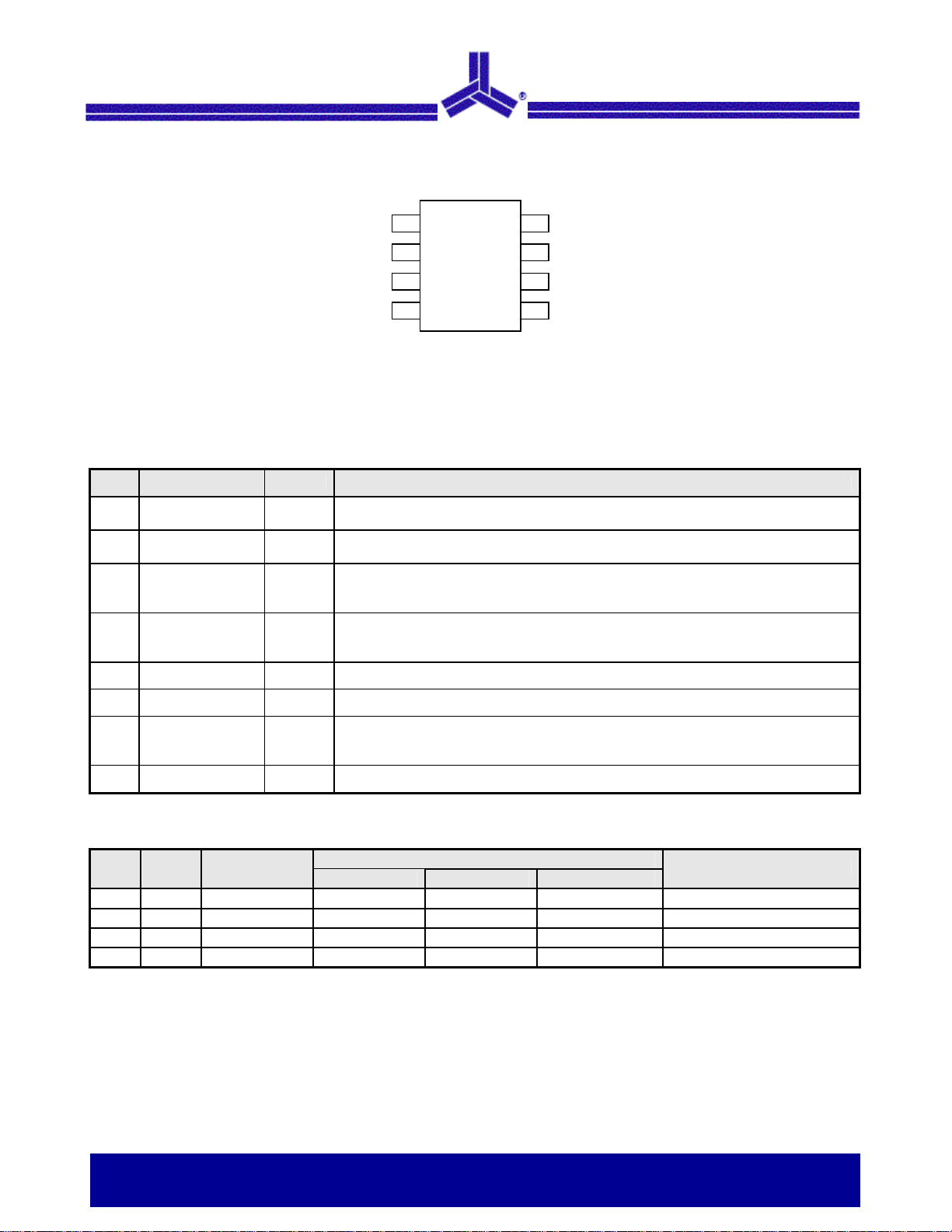
Pin Configuration
Pin Description (P278XA)
Pin# Pin Name Type Description
1 XIN/CLKIN I
2 XOUT O
3 FS1 I
4 LF I
5 VSS I Ground Connection. Connect to system ground.
XIN / CLKIN
XOUT
FS1
Connect to crystal or clock input. This pin has dual functions. It can be connected
either to an external crystal or an external reference clock.
Crystal connection. If using an external reference, this pin must be left
unconnected.
Digital logic input used to select input frequency range
(see the Input Frequency Selection Table). This pin has an internal pull-up
resistor.
External Loop Filter for the PLL. By changing the value of the CRC circuit, the
percentage spread can be adjusted accordingly. See the Loop Filter Selection
Table for detail value.
1
2
P278XA-08S
P278XA-08T
3
4
LF
Standard pin Configuration offered in both
8 pin SOIC and TSSOP Packages
8
7
6
5
VDD
FS0
ModOUT
VSS
6 ModOUT O Spread Spectrum Clock Output.
Digital logic input used to select input frequency range
7 FS0 I
8 VDD P Connect to +3.3 V
(see the Input Frequency Selection Table). This pin has an internal pull-up
resistor.
Input Frequency Selection Table
FS1 FS0 Input (MHz)
0 0 3 to 9 3 to 9 6 to 18 12 to 36 Fin / 128
0 1 10 to 19 10 to 19 20 to 38 40 to 76 Fin / 256
1 0 20 to 38 20 to 38 40 to 76 80 to 152 Fin / 512
1 1 39 to 78 39 to 78 78 to 156 156 to 312 Fin / 1024
Output Frequency Scaling (MHz)
P2781A P2782A P2784A
Modulation Rate (KHz)
General Purpose EMI Reduction IC 2 of 11
Notice: The information in this document is subject to change without notice.
Page 3
July 2005
P2781/82/84
rev 1.5
Loop Filter Selection Table VDD 3.3V
Contact Alliance for loop values that are not listed in the table and for component
selection values for industrial and automotive temperatures.
Input
FS1 FS0
MHz
3 0 0 270 330,000 220 270 330,000 300 270 100,000 390 560 100,000 510
4 0 0 270 100,000 270 270 100,000 390 270 100,000 560 560 100,000 680
5 0 0 270 100,000 390 270 100,000 560 270 100,000 750 560 100,000 910
6 0 0 270 100,000 510 270 100,000 750 270 10,000 1,000 680 6,800 1,200
7 0 0 270 100,000 620 270 100,000 1,000 270 5,600 1,200 330 3,300 1,200
8 0 0 270 100,000 820 270 100,000 1,200 270 12,000 2,200 680 6,800 2,200
9 0 0 270 100,000 1,000 270 100,000 1,500 270 5,600 2,200 270 2,700 2,200
10 0 1 270 100,000 330 270 100,000 510 270 100,000 750 560 100,000 910
11 0 1 270 100,000 390 270 100,000 560 270 100,000 866(1%) 560 100,000 1,100
12 0 1 270 100,000 510 270 100,000 750 270 10,000 1,000 680 6,800 1,200
13 0 1 270 100,000 560 270 100,000 820 270 12,000 1,200 470 4,700 1,200
14 0 1 270 100,000 620 270 100,000 1,000 270 5,600 1,200 330 3,300 1,200
15 0 1 270 100,000 750 270 100,000 1,100 270 3,900 1,200 330 3,300 1,500
16 0 1 270 100,000 820 270 100,000 1,200 270 12,000 2,200 680 6,800 2,200
17 0 1 270 100,000 910 270 100,000 1,300 270 10,000 2,200 390 3,900 2,200
18 0 1 270 100,000 1,000 270 100,000 1,500 270 5,600 2,200 270 2,700 2,200
19 0 1 270 100,000 1,200 270 100,000 1,600 270 3,300 2,200 270 2,700 2,700
20 0 0 270 100,000 330 270 100,000 560 270 100,000 750 560 100,000 910
21-22 1 0 270 100,000 390 270 100,000 620 270 100,000 866 (1%) 560 100,000 1,100
23-24 1 0 270 100,000 510 270 100,000 750 270 10,000 1,000 680 6,800 1,200
25-26 1 0 270 100,000 560 270 100,000 820 270 12,000 1,200 470 4,700 1,200
27-28 1 0 270 100,000 620 270 100,000 1,000 270 6,800 1,200 330 3,300 1,200
29-30 1 0 270 100,000 750 270 100,000 1,100 270 3,900 1,200 330 3,300 1,500
31-32 1 0 270 100,000 820 270 100,000 1,200 270 12,000 2,200 680 6,800 2,200
33-34 1 0 270 100,000 910 270 100,000 1,300 270 10,000 2,200 390 3,900 2,200
35-36 1 0 270 100,000 1,000 270 100,000 1,500 270 5,600 2,200 270 2,700 2,200
37-38 1 0 270 100,000 1,200 270 100,000 1,600 270 3,300 2,200 270 2,700 2,700
39-42 1 1 270 100,000 330 270 100,000 560 270 100,000 750 560 100,000 910
43-46 1 1 270 100,000 390 270 100,000 620 270 100,000 866 (1%) 560 100,000 1,100
47-50 1 1 270 100,000 510 270 100,000 750 270 10,000 1,000 680 6,800 1,200
51-54 1 1 270 100,000 560 270 100,000 820 270 12,000 1,200 470 4,700 1,200
55-58 1 1 270 100,000 620 270 100,000 1,000 270 6,800 1,200 330 3,300 1,200
59-62 1 1 270 100,000 750 270 100,000 1,100 270 3,900 1,200 330 3,300 1,500
63-66 1 1 270 100,000 820 270 100,000 1,200 270 12,000 2,200 680 6,800 2,200
67-70 1 1 270 100,000 910 270 100,000 1,300 270 8,200 2,200 390 3,900 2,200
71-74 1 1 270 100,000 1,000 270 100,000 1,600 270 5,600 2,200 270 2,700 2,200
75-78 1 1 270 100,000 1,200 270 100,000 1,800 270 3,300 2,200 270 2,700 2,700
1 The BW value is representative of typical conditions
BW = ±0.50%1 BW = ±0.75%1 BW = ±1.00%1 BW = ±1.25%1
C1
(pF)
C2
(pF)
R1
(ohm)
C1
(pF)
C2
(pF)
R1
(ohm)
C1
(pF)
C2
(pF)
R1
(ohm)
C1
(pF)
C2
(pF)
R1
(ohm)
General Purpose EMI Reduction IC 3 of 11
Notice: The information in this document is subject to change without notice.
Page 4
July 2005
P2781/82/84
rev 1.5
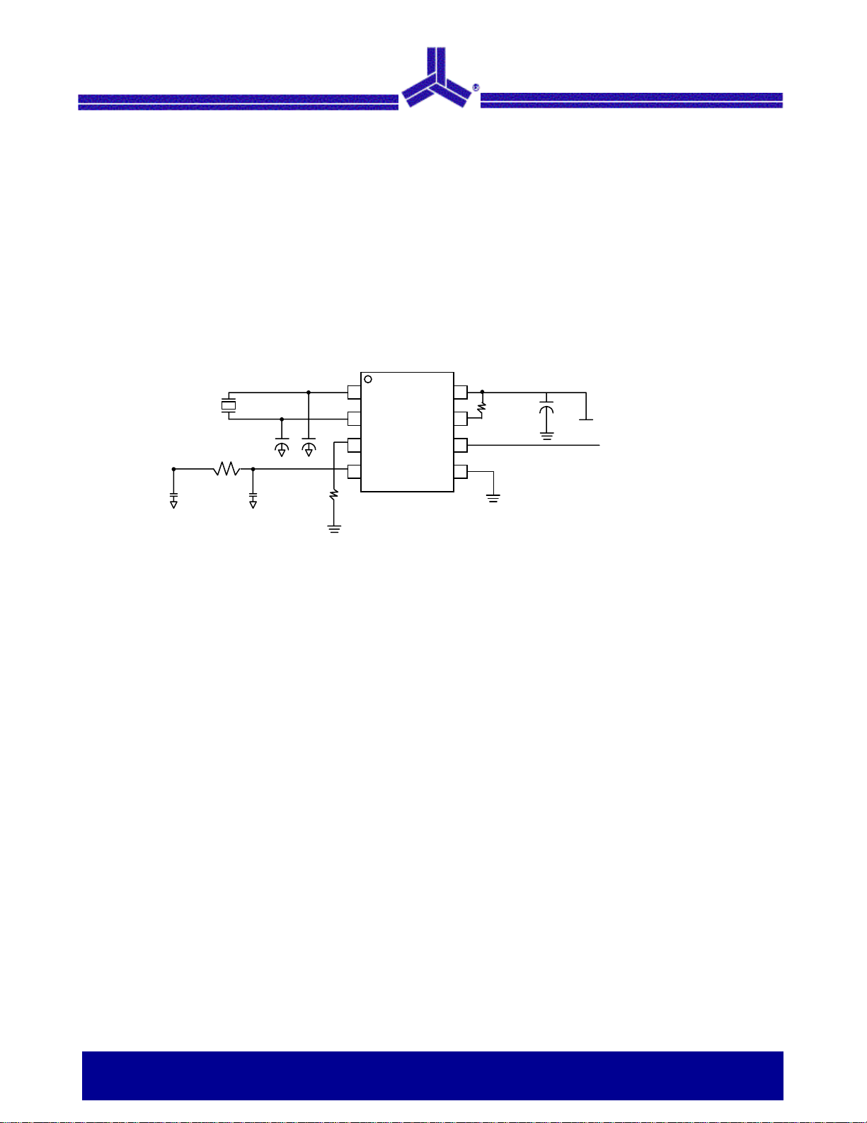
Spread Spectrum Selection
The P278xA performs Zero Cycle Slip when set at low percentage spreading. This allows no occurrence of system timing
error. The optimal setting should minimize system EMI to the fullest without affecting system performance. The spreading is
described as a percentage deviation of the center frequency.
(Note: the center frequency is the frequency of the external reference input on CLKIN, Pin 1.)
The P2781A is designed for PC peripheral, networking, notebook PC, and LCD monitor applications. It is optimized for
operation between 3 to 78MHz range. In the following application schematic example, the P2781A spread percentage
selection is determined by the external LF value specified in the Loop Filter Selection Table. The Input Frequency Selection
Table specifies the input frequency range. The external LF allows the user to fine tune the spread percentage to optimize the
EMI reduction benefits of the spread spectrum.
C2 C1
Note: Both logic input pins FS1 and FS0 have to be connected to either VDD or VSS. Do not leave them floating.
16 MHz
R1
0 Ohm
XIN/CLKIN
1
XOUT
2
FS1
3
4
ModOUT
P2781A
VDD
FS0
VSSLF
8
2.2 K
7
6
5
0.1µF
+3.3V
Modulated 16MHz Clock
To target Chip
General Purpose EMI Reduction IC 4 of 11
Notice: The information in this document is subject to change without notice.
Page 5

July 2005
P2781/82/84
rev 1.5
Absolute Maximum Ratings
Symbol Parameter Rating Unit
VDD Supply voltage, DC (VSS – 0.5) to 7 V
VI Input voltage, DC (VSS-0.5) to (VDD+0.5) V
VO Output voltage, DC (VSS-0.5) to (VDD + 0.5) V
IIK Input clamp current (VI<0 or VI>VDD) -50 to +50 mA
IOK Output clamp current (VI<0 or VI>VDD) -50 to +50 mA
TS Storage temperature -65 to +125 °C
TA Ambient temperature range, under bias -55 to 125 °C
TJ Junction temperature 150 °C
Lead temperature (soldering 10 sec) 260 °C
Input static discharge voltage protection
Note: These are stress ratings only and functional operation is not implied. Exposure to absolute maximum ratings for extended periods may affect device
reliability.
(As per JEDEC STD22- A114-B)
DC Electrical Characteristics
(Test condition: All parameters are measured at room temperature (+25°C) unless otherwise stated)
Symbol Parameter Min Typ Max Unit
VIL Input low voltage VSS – 0.3 - 0.8 V
V
Input high voltage 2.0 - VDD +0.3 V
IH
IIL
IIH
I
XOL
I
XOUT output high current - 10 - mA
XOH
Input low current
(internal input pull-up resistor on FS0 and FS1)
Input high current
(internal input pull-up resistor on FS0 and FS1)
XOUT output low current - 10 - mA
2 kV
- 60 - µA
- 60 - µA
V
Output low voltage (VDD = 3.3V, IOL = 20mA) - - 0.4 V
OL
V
Output high voltage (VDD = 3.3V, IOH = 20mA) 2.5 - - V
OH
I
Static supply current - 3 - mA
DD
ICC
Typical dynamic supply current
(25pF scope probe loading)
5.2 at 3MHz - 21.2 at 82MHz mA
VDD Operating voltage 3.0 3.3 3.6 V
General Purpose EMI Reduction IC 5 of 11
Notice: The information in this document is subject to change without notice.
Page 6

July 2005
P2781/82/84
rev 1.5
AC Electrical Characteristics
Symbol Parameter Min Typ Max Unit
fIN Input frequency: P278XA 3 - 78 MHz
f
OUT
tLH
P278XA
tHL
P278XA
t
P2781A
tD
P2781A
∆F
P278XA
Output frequency:
Output rise time (measured at 0.8 V to 2.0 V,
25pF scope probe loading)
Output fall time (measured at 2.0 V to 0.8 V, 25
pF scope probe loading)
JC
Jitter (cycle to cycle, ± 6sigma, 1000 sweeps,
± 0.5% spread, I/O frequency = 16MHz)
Output duty cycle deviation (error from 50% duty
cycle, 25pF scope probe loading)
Frequency deviation tolerance from BW% stated
in the Loop Filter Selection Table
P2781A
P2782A
P2784A
3
6
12
- 1 - nS
- 1 - nS
- ±250 - pS
±1 at 3MHz - ±2 at 82MHz %
-20 0 +20 %
-
78
156
312
MHz
General Purpose EMI Reduction IC 6 of 11
Notice: The information in this document is subject to change without notice.
Page 7

C
July 2005
P2781/82/84
rev 1.5
Package Information
Mechanical Package Outline 8-Pin SOIC Package
H
E
D
A2
A
e
B
A1
D
θ
Dimensions
Symbol
Inches
Millimeters
Min Max Min Max
L
A1 0.004 0.010 0.10 0.25
A 0.053 0.069 1.35 1.75
A2 0.049 0.059 1.25 1.50
B 0.012 0.020 0.31 0.51
C 0.007 0.010 0.18 0.25
D 0.193 BSC 4.90 BSC
E 0.154 BSC 3.91 BSC
e 0.050 BSC 1.27 BSC
H 0.236 BSC 6.00 BSC
L 0.016 0.050 0.41 1.27
θ 0° 8° 0° 8°
Note: Controlling dimensions are millimeters
SOIC - 0.074 grams unit weight
General Purpose EMI Reduction IC 7 of 11
Notice: The information in this document is subject to change without notice.
Page 8

C
July 2005
rev 1.5
P2781/82/84
Mechanical Package Outline 8-Pin TSSOP Package
H
E
D
e
B
A2
A
θ
A1
L
Symbol
Inches Millimeters
Min Max Min Max
A
A1 0.002 0.006 0.05 0.15
A2 0.033 0.037 0.85 0.95
B 0.008 0.012 0.19 0.30
c 0.004 0.008 0.09 0.20
D 0.114 0.122 2.90 3.10
E 0.169 0.177 4.30 4.50
e 0.026 BSC 0.65 BSC
H 0.252 BSC 6.40 BSC
L 0.020 0.028 0.50 0.70
θ 0° 8° 0° 8°
Note: Controlling dimensions are millimeters
TSSOP - 0.0325 grams unit weight
Dimensions
0.043
1.10
General Purpose EMI Reduction IC 8 of 11
Notice: The information in this document is subject to change without notice.
Page 9

July 2005
P2781/82/84
rev 1.5
Ordering Codes
Ordering # Marking Package Type QTY / Reel Temperature
P278XA-08ST P278XA 8 PIN SOIC, TUBE See flow
P278XA-08SR P278XA 8 PIN SOIC, TAPE & REEL 2,500 See flow
P278XA-08TT P278XA 8 PIN TSSOP, TUBE See flow
P278XA-08TR P278XA 8 PIN TSSOP, TAPE & REEL 2,500 See flow
P278XAF-08ST P278XAF 8 PIN SOIC, TUBE, Pb Free See flow
P278XAF-08SR P278XAF 8 PIN SOIC, TAPE AND REEL,Pb Free 2,500 See flow
P278XAF-08TT P278XAF 8 PIN TSSOP, TUBE, Pb Free See flow
P278XAF-08TR P278XAF 8 PIN TSSOP, TAPE AND REEL, Pb Free 2,500 See flow
P278XAG-08ST P278XAG 8 PIN SOIC, TUBE, Green See flow
P278XAG-08SR P278XAG 8 PIN SOIC, TAPE AND REEL, Green 2,500 See flow
P278XAG-08TT P278XAG 8 PIN TSSOP, TUBE, Green See flow
P278XAG-08TR P278XAG 8 PIN TSSOP, TAPE AND REEL, Green 2,500 See flow
I278XA-08ST I278XA 8 PIN SOIC, TUBE See flow
I278XA-08SR I278XA 8 PIN SOIC, TAPE & REEL 2,500 See flow
I278XA-08TT I278XA 8 PIN TSSOP, TUBE See flow
I278XA-08TR I278XA 8 PIN TSSOP, TAPE & REEL 2,500 See flow
I278XAF-08ST I278XAF 8 PIN SOIC, TUBE, Pb Free See flow
I278XAF-08SR I278XAF 8 PIN SOIC, TAPE AND REEL,Pb Free 2,500 See flow
I278XAF-08TT I278XAF 8 PIN TSSOP, TUBE, Pb Free See flow
I278XAF-08TR I278XAF 8 PIN TSSOP, TAPE AND REEL, Pb Free 2,500 See flow
I278XAG-08ST I278XAG 8 PIN SOIC, TUBE, Green See flow
I278XAG-08SR I278XAG 8 PIN SOIC, TAPE AND REEL, Green 2,500 See flow
I278XAG-08TT I278XAG 8 PIN TSSOP, TUBE, Green See flow
I278XAG-08TR I278XAG 8 PIN TSSOP, TAPE AND REEL, Green 2,500 See flow
X278XA-08ST X278XA 8 PIN SOIC, TUBE See flow
X278XA-08SR X278XA 8 PIN SOIC, TAPE & REEL 2,500 See flow
X278XA-08TT X278XA 8 PIN TSSOP, TUBE See flow
X278XA-08TR X278XA 8 PIN TSSOP, TAPE & REEL 2,500 See flow
X278XAF-08ST X278XAF 8 PIN SOIC, TUBE, Pb Free See flow
X278XAF-08SR X278XAF 8 PIN SOIC, TAPE AND REEL, Pb Free 2,500 See flow
X278XAF-08TT X278XAF 8 PIN TSSOP, TUBE, Pb Free See flow
X278XAF-08TR X278XAF 8 PIN TSSOP, TAPE AND REEL, Pb Free 2,500 See flow
X278XAG-08ST X278XAG 8 PIN SOIC, TUBE, Green See flow
X278XAG-08SR X278XAG 8 PIN SOIC, TAPE AND REEL, Green 2,500 See flow
X278XAG-08TT X278XAG 8 PIN TSSOP, TUBE, Green See flow
X278XAG-08TR X278XAG 8 PIN TSSOP, TAPE AND REEL, Green 2,500 See flow
General Purpose EMI Reduction IC 9 of 11
Notice: The information in this document is subject to change without notice.
Page 10

p
July 2005
P2781/82/84
rev 1.5
Device Ordering Information
P278XA F- 08 XX
Package:
ST – SOIC, TUBE
SR - SOIC, T/R
TT – TSSOP, TUBE
TR - TSSOP, T/R
Pin Count
F = LEAD FREE or RoHS COMPLIANT PART
G = GREEN
DEVICE NUMBER
Licensed under US patent #5,488,627, #6,646,463 and #5,631,920
Flow:
P = Commercial Temperature Range (0°C to 70°C)
I = Industrial Temperature Range (-40°C to 85°C)
X = Automotive Tem
erature Range (-40°C to 125°C)
General Purpose EMI Reduction IC 10 of 11
Notice: The information in this document is subject to change without notice.
Page 11

July 2005
P2781/82/84
rev 1.5
Alliance Semiconductor Corporation
2575, Augustine Drive,
Santa Clara, CA 95054
Tel# 408-855-4900
Fax: 408-855-4999
www.alsc.com
Note: This product utilizes US Patent # 6,646,463 Impedance Emulator Patent issued to Alliance Semiconductor, dated 11-11-2003
© Copyright 2003 Alliance Semiconductor Corporation. All rights reserved. Our three-point logo, our name and Intelliwatt are
trademarks or registered trademarks of Alliance. All other brand and product names may be the trademarks of their
respective companies. Alliance reserves the right to make changes to this document and its products at any time without
notice. Alliance assumes no responsibility for any errors that may appear in this document. The data contained herein
represents Alliance's best data and/or estimates at the time of issuance. Alliance reserves the right to change or correct this
data at any time, without notice. If the product described herein is under development, significant changes to these
specifications are possible. The information in this product data sheet is intended to be general descriptive information for
potential customers and users, and is not intended to operate as, or provide, any guarantee or warrantee to any user or
customer. Alliance does not assume any responsibility or liability arising out of the application or use of any product
described herein, and disclaims any express or implied warranties related to the sale and/or use of Alliance products
including liability or warranties related to fitness for a particular purpose, merchantability, or infringement of any intellectual
property rights, except as express agreed to in Alliance's Terms and Conditions of Sale (which are available from Alliance).
All sales of Alliance products are made exclusively according to Alliance's Terms and Conditions of Sale. The purchase of
products from Alliance does not convey a license under any patent rights, copyrights; mask works rights, trademarks, or any
other intellectual property rights of Alliance or third parties. Alliance does not authorize its products for use as critical
components in life-supporting systems where a malfunction or failure may reasonably be expected to result in significant
injury to the user, and the inclusion of Alliance products in such life-supporting systems implies that the manufacturer
assumes all risk of such use and agrees to indemnify Alliance against all claims arising from such use.
Copyright © Alliance Semiconductor
All Rights Reserved
Part Number: P2781/82/84
Document Version: 1.5
General Purpose EMI Reduction IC 11 of 11
Notice: The information in this document is subject to change without notice.
Page 12

 Loading...