

Page 1
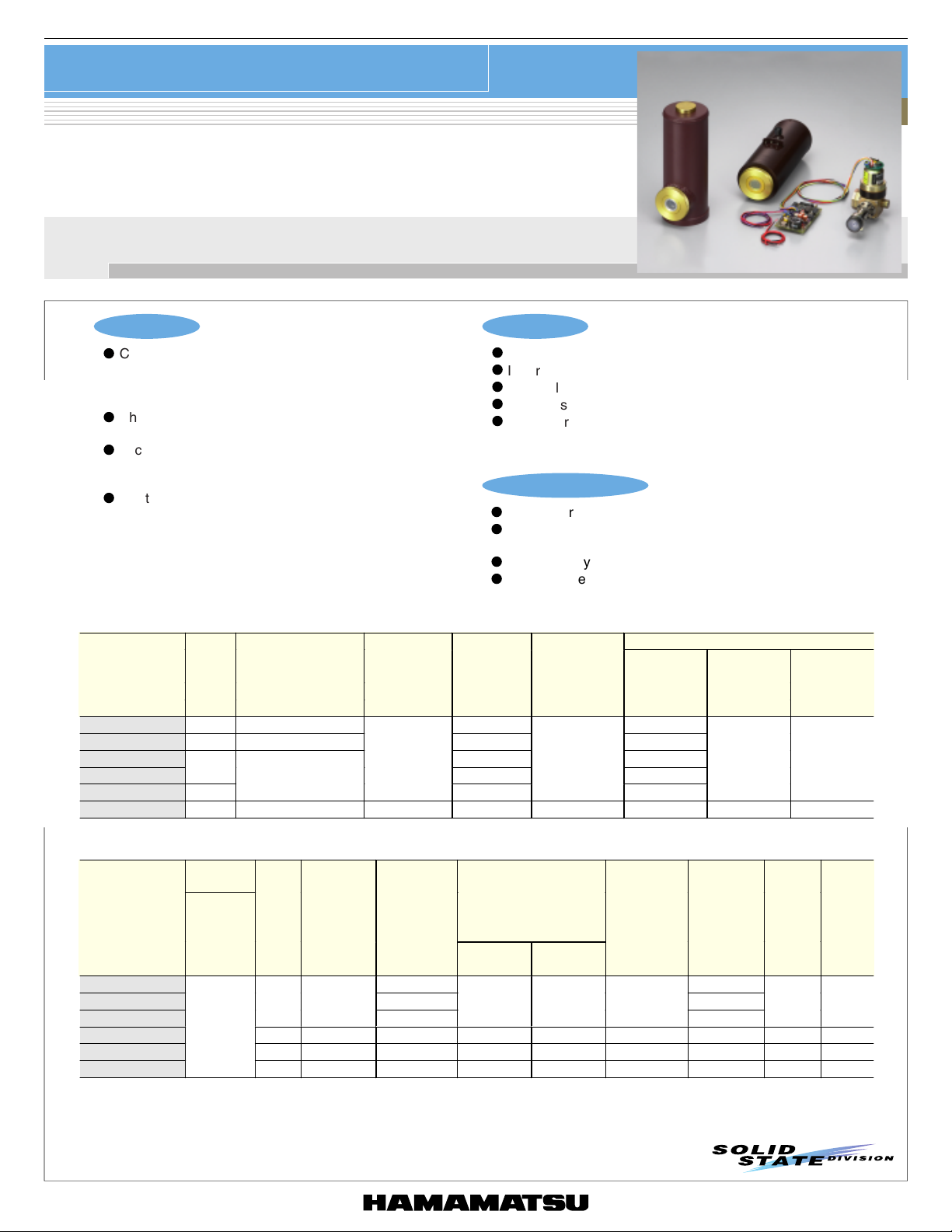
INFRARED DETECTOR
MCT photoconductive detector
P2748/P5274 series
,
P3257-50
Dewar type detector with high sensitivity and high-speed response in long wavelength range
Features
l
Choice of spectral response range (up to 25 µm)
The band gap can be adjusted by controlling the composition
ratio of HgTe and CdTe. Utilizing this fact, various types are
available in different spectral characteristics.
l
Photoconductive element that decreases its resistance
by input of infrared light
l
Micro-cooled type available
This type of cooling does not require pour-filled liquid
nitrogen.
l
Custom devices available
Custom devices not listed in this catalog are also available
with different spectral response, active area sizes and
number of elements.
Glass dewar type not requiring repumping is also provided.
■ General rating / Absolute maximum ratings
Dimensional
Type No.
P2748-40
P2748-41
P2748-42 0.25 × 0.25 20
P5274
P5274-01
P3257-50
outline/
Window
materi al *
/Z
➀
/Z
➁
/Z
➀
/K
➀
/Z Stirling type metal Micro-cooled 1 × 1 - 40 -40 to +55 -45 to +55
➂
Package Cooling
Side-on type metal dewar
Head-on type metal dewar
Side-on type metal dewar
LN
Applications
l
FTIR
l
Infrared spectrophotometer
l
Thermal imaging
l
Remote sensing
l
2
laser detection
CO
Accessories (Optional)
l
Valve operator A3515
l
Amplifiers for dewar type MCT photoconductive detector
l
Power supply for amplifier C3871
l
Infrared detector module with preamp P7752-10
Nitrogen
Active area
(mm)
1 × 1 40
1 × 1 40
1 × 1 40
1 × 1
maintenance
time
Min.
(h) (mA)
12
Absolute maximum ratings
Allowable
current
20
Operating
temperature
Topr
(°C)
-40 to +60 -55 to +60
C5185
Storage
temperature
Tstg
(°C)
■ Electrical and optical characteristics (Typ. unless otherwise noted)
Measurement
condition
Ele ment
Type No.
P2748-40 1000 2.5 × 10
P2748-41 1000 2.5 × 10
P2748-42
P5274 14 17 500 2 × 10
P5274-01 17 22 250 1 × 10
P3257-50
*1: Window material K: KRS-5, Z: ZnSe
*2: Photo sensitivity changes with the bias current. The values in the above table are measured with the optimum bias current.
temperature
T
(°C) (µm) (µm) (V/W)
-196
Peak
sensitivity
wavelength
lp
12 14
12 14 1000 1 × 10
Cut-off
wavelength
lc
Photo
sensitivity *
S
l=lp
10000
2
(cm·Hz
1 × 10
*
D
(500, 1200, 1)
Min.
1/2
/W)
(cm·Hz
10
2 × 10
9
1 × 10
9
5 × 1091.0 × 10101.0 × 10
10
2 × 10
Typ.
1/2
*
D
(lp, 1200, 1)
/W) (cm·Hz
10
10
10
1/2
/W)
4.0 × 10
1.5 × 10106.7 × 10
4.0 × 10102.5 × 10
10
NEP
l=lp
(W/Hz
6.3 × 10
Rise
time
tr
0 to 63 %
1/2
)(µs)
-12
-12
0.6 40
-12
-12
0.6 30
-11
0.4 100
-12
0.6 40
Dark
resist ance
Rd
(W)
1
Page 2
MCT photoconductive detector
P2748/P5274 series, P3257-50
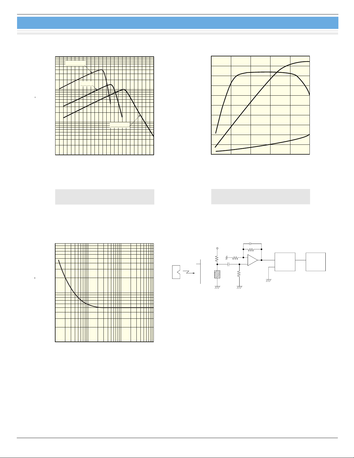
■ Spectral response
11
10
P2748-40
10
10
/W)
1
2
9
10
D* (cm · Hz
8
10
0 5 10 15 20 25
Spectral response can be shifted upon
request.
P5274
P5274-01
WAVELENGTH (µm)
(Typ. T= -196 ˚C)
KIRDB0072EC
■ S/N vs. bias current
20
16
12
8
RELATIVE VALUE
4
0 5 10 20 25
BIAS CURRENT (mA)
The detector must be operated in a range
where the D* becomes Max.
(Typ.)
D*
S
N
15
KIRDB0073EB
■ Noise frequency characteristic
100
1
2
10
NOISE (nV/Hz )
1
10 100
FREQUENCY (Hz)
(Typ. )
1000 10000
KIRDB0074EC
■ Measurement circuit
CHOPPER
1200 Hz
BLACK BODY
500 K
DETECTOR
BAND-PASS
FILTER
fo=1200 Hz
∆f=120 Hz
INCIDENT ENERGY: 2.64 µW/cm
r.m.s.
METER
KIRDC0007EA
2
2
Page 3
MCT photoconductive detector
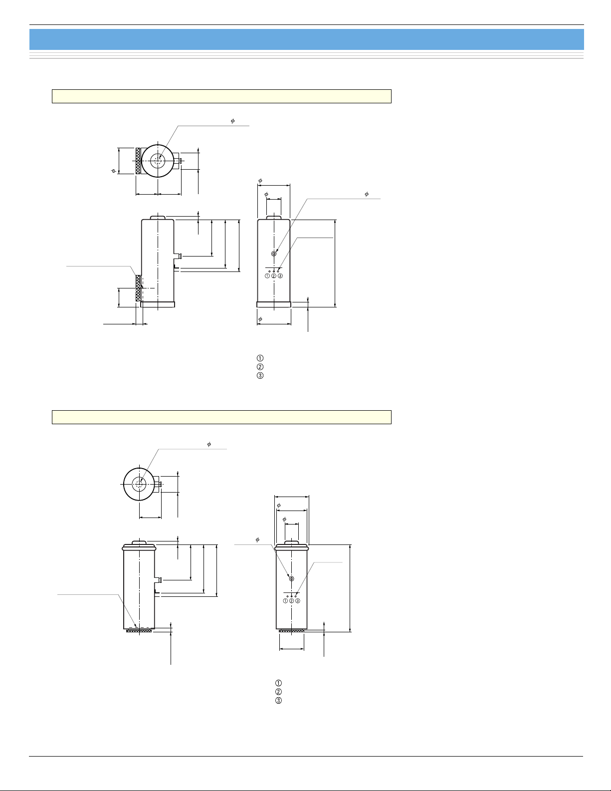
■ Dimensional outlines (unit: mm)
➀ P2748-40/-42, P5274 series
LN2 FILL PORT 12.5
51 ± 1
46 ± 143 ± 1
32 ± 1
P2748/P5274 series, P3257-50
63.5 ± 1
28.5
PUMP-OUT PIPE 9.5
PHOTOSENSITIVE
SURFACE
8.5 ± 0.5
➁ P2748-41
PHOTOSENSITIVE
SURFACE
37 ± 1
LN2 FILL PORT 12.5
46 ± 1
32 ± 16.5
6.5
70 ± 2
72 ± 1
95 ± 2
95 ± 1
102 ± 2
SIGNAL
OUTPUT LEAD
102 ± 1
172 ± 2
66.8 ± 1
10 ± 1
DETECTOR
NC
DETECTOR
KIRDA0131EC
66 MAX.
63.5 ± 1
28.5
PUMP-OUT
PORT 9.5
OUTPUT
PIN
172 ± 2
8.5 ± 0.5
51.2 ± 1
7.9 ± 1
DETECTOR
NC
DETECTOR
KIRDA0129EA
3
Page 4
MCT photoconductive detector
R
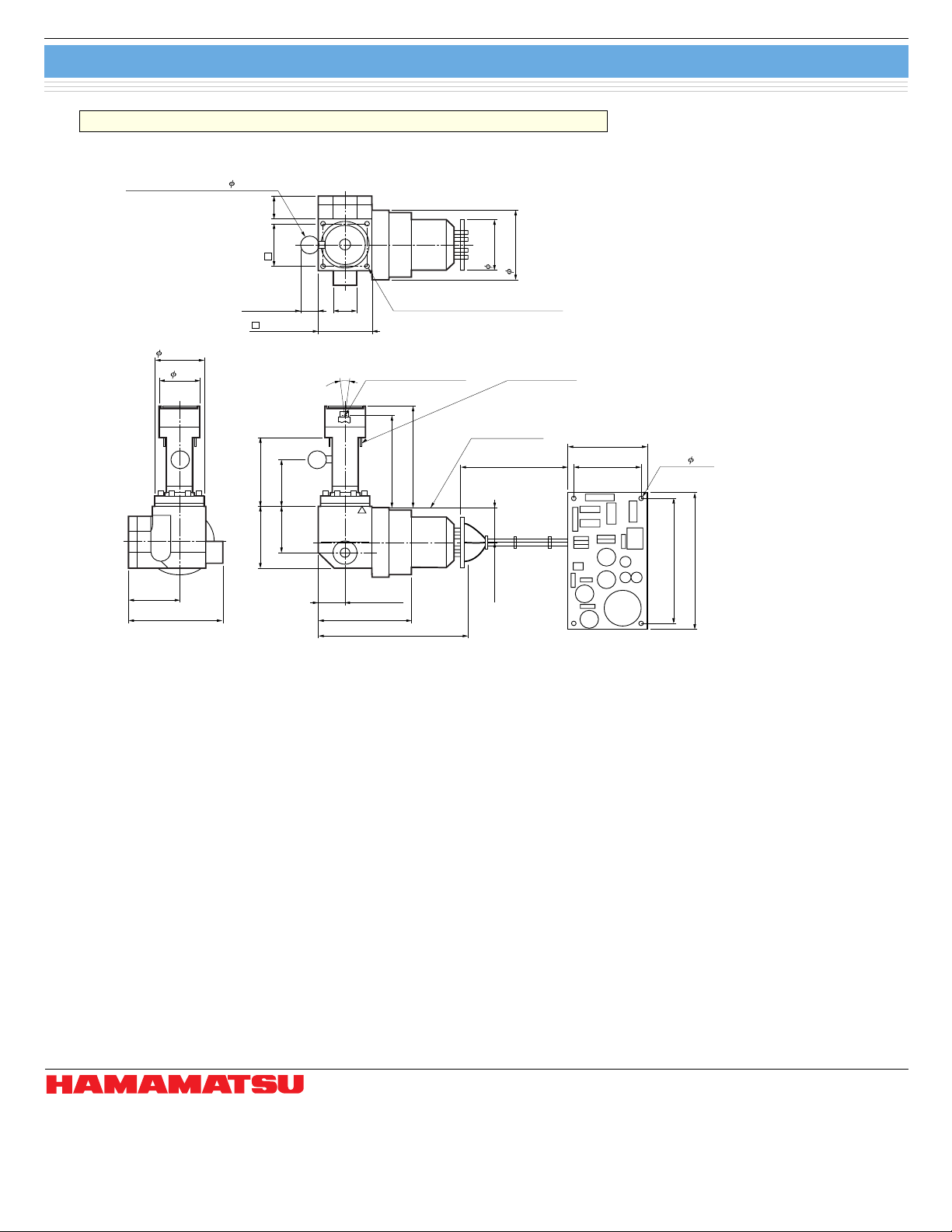
➂ P3257-50
PUMP-OUT VALVE 10 MAX.
12.8
P2748/P5274 series, P3257-50
26.7
27.4 MAX.
50.1 MAX.
23.8
10.6 MAX.
29.0 MAX.
+0
-0.01
22
12.7
FOV
(2 ×) 56UNC-2B DEPTH: 5.5 4PL
MOUNTING HOLE
PHOTOSENSITIVE
SURFACE
56.0 ± 0.3
50.8 ± 0.1
28.3 MAX.
38.9 MAX.
OUTPUT PIN
MOUNT SIDE
58 36.4
43
(4 ×) 2.5
25.9 26.8
34.8 MAX. 39.4
14.5 MAX.
50.3 MAX.
81.1 MAX.
20.1 MAX.
Board thickness including
mounted components: 20 MAX.
70.0
76.5
KI
KIRDA0130EA
Information furnished by HAMAMATSU is believed to be reliable. However, no responsibility is assumed for possible inaccuracies or omissions.
HAMAMATSU PHOTONICS K.K., Solid State Division
1126-1 Ichino-cho, Hamamatsu City, 435-8558 Japan, Telephone: (81) 053-434-3311, Fax: (81) 053-434-5184, http://www.hamamatsu.com
U.S.A.: Hamamatsu Corporation: 360 Foothill Road, P.O.Box 6910, Bridgewater, N.J. 08807-0910, U.S.A., Telephone: (1) 908-231-0960, Fax: (1) 908-231-1218
Germany: Hamamatsu Photonics Deutschland GmbH: Arzbergerstr. 10, D-82211 Herrsching am Ammersee, Germany, Telephone: (49) 08152-3750, Fax: (49) 08152-2658
France: Hamamatsu Photonics France S.A.R.L.: 8, Rue du Saule Trapu, Parc du Moulin de Massy, 91882 Massy Cedex, France, Telephone: 33-(1) 69 53 71 00, Fax: 33-(1) 69 53 71 10
United Kingdom: Hamamatsu Photonics UK Limited: 2 Howard Court, 10 Tewin Road, Welwyn Garden City, Hertfordshire AL7 1BW, United Kingdom, Telephone: (44) 1707-294888, Fax: (44) 1707-325777
North Europe: Hamamatsu Photonics Norden AB: Smidesvägen 12, SE-171 41 Solna, Sweden, Telephone: (46) 8-509-031-00, Fax: (46) 8-509-031-01
Italy: Hamamatsu Photonics Italia S.R.L.: Strada della Moia, 1/E, 20020 Arese, (Milano), Italy, Telephone: (39) 02-935-81-733, Fax: (39) 02-935-81-741
4
Specifications are subject to change without notice. No patent rights are granted to any of the circuits described herein. ©2002 Hamamatsu Photonics K.K.
Cat. No. KIRD1021E03
Oct. 2002 DN
 Loading...