

Page 1
查询P2681A供应商
October 2003 P2681A
rev D
General Purpose EMI Reduction IC
Features
FCC approved method of EMI attenuation
Provides up to 15 dB of EMI suppression
Generates a 1 X or ½ X low EMI spread
spectrum clock of the input frequency
Output frequency from 6MHz to 20MHz
Digital spread selections
Spreading ranges from +/-0.4% to +/-5.0%
Ultra low cycle-to-cycle jitter
Zero-cycle slip
3.3V and 5.0V operating voltage range
10 mA output drives
TTL or CMOS compatible outputs
Ultra-low power CMOS design
Available in 8 pin SOIC and TSSOP
Product Description
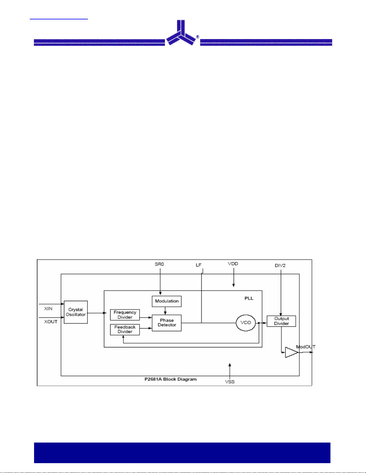
The P2681A is a versatile spread spectrum
frequency modulator designed specifically for digital
camera and other digital video and imaging
applications. The P2681A reduces electromagnetic
interference (EMI) at the clock source, which
provides system wide reduction of EMI of all clock
dependent signals. The P2681A allows significant
Block Diagram
system cost savings by reducing the number of circuit
board layers and shielding that are traditionally
required to pass EMI regulations.
The P2681A uses the most efficient and optimized
modulation profile approved by the FCC.
The P2681A modulates the output of a single PLL in
order to “spread” the bandwidth of a synthesized
clock and, more importantly, decreases the peak
amplitudes of its harmonics. This results in
significantly lower system EMI compared to the
typical narrow band signal produced by oscillators
and most frequency generators. Lowering EMI by
increasing a signal’s bandwidth is called “spread
spectrum clock generation”.
Applications
The P2681A is targeted towards MFP, xDSL, fax
modem, set-top box, USB controller, DSC, and
embedded systems.
2575, Augustine Drive • Santa Clara, CA • Tel: 408.855.4900 • Fax: 408.855.4999 • www.alsc.com
Notice: The information in this document is subject to change without notice.
Alliance Semiconductor
Page 2

October 2003 P2681A
rev D
Pin Configuration
Pin Description
Pin# Pin Name Type Description
1 XIN/CLKIN I Connect to crystal or clock input.
2 XOUT I Crystal output
Digital logic input used to select normal output mode or divide-by-2 output
3 DIV2 I
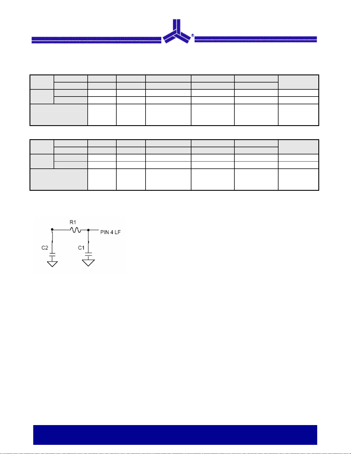
4 LF I
5 VSS I Ground Connection. Connect to system ground.
6 ModOUT O Spread Spectrum Clock Output.
7 SR0 I
8 VDD P Connect to +3.3V or 5.0V
mode. When this pin is Low, the frequency of the output clock is the same
as the input clock frequency. When it is tied High, the output frequency is
half the input clock frequency. This pin has an internal pull-low resistor.
External Loop Filter for the PLL. By changing the value of the CRC circuit,
the % spread can be adjusted accordingly. See Table 1.2 for detail value.
Digital logic input used to select Spreading Range between large or small
for a given LF value (see Table 1.1 and 1.2). When SR0=0, the spreading %
is smaller than SR0=1. This pin has an internal pull-up resistor.
Notice: The information in this document is subject to change without notice.
General Purpose EMI Reduction IC 2 of 10
Page 3
October 2003 P2681A
rev D
Table 1 - Modulation Output and Spreading Selection VDD @ 3.3V
DIV=0
SR0
Loop filter value*
DIV=0
SR0
Loop filter value*
*For additional spread % selection please refer to Loop Filter Selection Table
Table 2 - Loop Filter Selection Table VDD @ 3.3V
Xin 6 MHz 8 MHz 10 MHz 12 MHz 16 MHz
ModOut 6 MHz 8 MHz 10 MHz 12 MHz 16 MHz
0
1
Xin 6 MHz 8 MHz 10 MHz 12 MHz 16 MHz
ModOut 3 MHz 4 MHz 5 MHz 6 MHz 8 MHz
0
1
TBD TBD +/-0.75% +/-0.75% +/-0.75% ModOut/256
TBD TBD +/-1.30% +/-1.30% +/-1.30% ModOut/256
C1=1,000 pF
TBD TBD
TBD TBD +/-0.75% +/-0.75% +/-0.75% ModOut/128
TBD TBD +/-1.30% +/-1.30% +/-1.30% ModOut/128
TBD TBD
C2=10,000 pF
R1=1K
C1=1,000 pF
C2=10,000 pF
R1=1K
C1=1,000 pF
C2=10,000 pF
R1=1.5K
C1=1,000 pF
C2=10,000 pF
R1=1.5K
C1=390 pF
C2=3,900 pF
R1=2.2K
C1=390 pF
C2=3,900 pF
R1=2.2K
Modulation
Rate
Modulation
Rate
Please contact Alliance Semiconductor for more information
General Purpose EMI Reduction IC 3 of 10
Notice: The information in this document is subject to change without notice.
Page 4

October 2003 P2681A
rev D
Spread Spectrum Selection
The P2681A performs Zero Cycle Slip when sets at low % spreading. This allows no occurrence of system
timing error. The optimal setting should minimize system EMI to the fullest without affecting system
performance. The spreading is described as a percentage deviation of the center frequency (Note: the center
frequency is the frequency of the external reference input on CLKIN, Pin 1).
Example: The P2681A is designed for PC peripheral applications. It is not only optimized for operation between
6MHz – 16MHz range, but its output frequency can be extended down to one half of the input clock frequency
using the Divide-by-Two feature. This feature extends low frequency operation to as low as 3MHz. Setting Pin 3
high (DIV2=1; Divide-by-Two mode) sets the output frequency (ModOUT) to half the frequency of the input clock
(CLKIN). This is a simple way to generate a spread spectrum modulated low frequency clock when only a
higher frequency signal is available. If you want the output frequency to be the same as the input, you need to
set DIV2=0.
The P2681A’s spread % selection is determined by the external LF value specified in Table 2. Table 1 provides
a particular LF value which allows the % spreading to be selected between +/-0.75% or +/-1.30% by setting SR0
to either 0 and 1. At a specified LF value (See Table 2), SR0 pin allows the user to have the flexibility to digitally
select between large or small % spreading by setting SR0=1 or SR0=0 respectively.
P2681A Application Schematic
Notice: The information in this document is subject to change without notice.
General Purpose EMI Reduction IC 4 of 10
Page 5

October 2003 P2681A
rev D
EMC Software Simulation
By using Alliance Semiconductor’s proprietary EMC simulation software – EMI-lator®, radiated system level EMI
analysis can be made easier to allow a quantitative assessment on Alliance’s EMI reduction products. The
simulation engine of this EMC software has already been characterized to correlate with the electrical
characteristics of Alliance EMI reduction IC’s. The figure below is an example of the simulation result. Please
visit our web site at www.alsc.com
Simulation Result from EMI-lator®
for information on how to obtain a free copy and demonstration of EMI-lator®.
Notice: The information in this document is subject to change without notice.
General Purpose EMI Reduction IC 5 of 10
Page 6

October 2003 P2681A
rev D
Absolute Maximum Ratings
Symbol Parameter Rating Unit
VDD, VIN Voltage on any pin with respect to GND
T
Storage temperature
STG
TA Operating temperature
DC Electrical Characteristics
Symbol Parameter Min Typ Max Unit
VIL Input Low Voltage GND – 0.3 - 0.8 V
VIH Input High Voltage 2.0 - VDD + 0.3 V
IIL
IIH
IXOL XOUT Output Low Current (@ 0.4V, VDD = 3.3V) - TBD - mA
IXOH XOUT Output High Current (@ 2.5V, VDD = 3.3V) - TBD - mA
Input Low Current (internal input pull-up resistor on
DIV2 and SR0)
Input High Current (internal input pull-up resistor on
DIV2 and SR0)
-0.5 to + 7.0 V
-65 to +125 °C
0 to +70 °C
- TBD -
- TBD -
µA
µA
VOL Output Low Voltage (VDD = 3.3V, IOL = 20 mA) - - 0.4 V
VOH Output High Voltage (VDD = 3.3V, IOH = 20 mA) 2.5 - - V
IDD Static Supply Current - TBD - mA
ICC
VDD Operating Voltage TBD 3.3 TBD V
AC Electrical Characteristics
Symbol Parameter Min Typ Max Unit
fIN Input Frequency when
tLH*
tHL*
tJC Jitter (cycle to cycle) - - TBD ps
*tLH and tHL are measured into a capacitive load of 15pF
Dynamic Supply Current
(3.3V and 10 pF loading)
Output rise time
(Measured at 0.8V to 2.0V)
Output fall time
(Measured at 0.8V to 2.0V)
tD Output duty cycle 45 50 55 %
3
Xin=6MHz
6 - 20 MHz
TBD ns
TBD ns
TBD
15
Xin=20MHz
mA
Notice: The information in this document is subject to change without notice.
General Purpose EMI Reduction IC 6 of 10
Page 7

October 2003 P2681A
rev D
Package Information
Mechanical Package Outline 8-Pin SOIC
Dimensions in inches Dimensions in millimeters
Symbol
Min Nor Max Min Nor Max
A 0.057 0.064 0.071 1.45 1.63 1.80
A1 0.004 0.007 0.010 0.10 0.18 0.25
A2 0.053 0.061 0.069 1.35 1.55 1.75
B 0.012 0.016 0.020 0.31 0.41 0.51
C 0.004 0.006 0.01 0.10 0.15 0.25
D 0.186 0.194 0.202 4.72 4.92 5.12
E 0.148 0.156 0.164 3.75 3.95 4.15
e 0.050 BSC 1.27 BSC
H 0.224 0.236 0.248 5.70 6.00 6.30
L 0.012 0.020 0.028 0.30 0.50 0.70
a 0° 5° 8° 0° 5° 8°
Note: Controlling dimensions are millimeters
Notice: The information in this document is subject to change without notice.
General Purpose EMI Reduction IC 7 of 10
Page 8

October 2003 P2681A
rev D
Mechanical Package Outline 8-Pin TSSOP
Symbol Min Nor Max Min Nor Max
A
A1 0.002
A2 0.031 0.039 0.041 0.80 1.00 1.05
B 0.007 0.012 0.19 0.30
C 0.004 0.008 0.09 0.20
D 0.114 0.118 0.122 2.90 3.00 3.10
E 0.169 0.173 0.177 4.30 4.40 4.50
e 0.026 BSC 0.65 BSC
H 0.244 0.252 0.260 6.20 6.40 6.60
L 0.018 0.024 0.030 0.45 0.60 0.75
a 0°
Note: Controlling dimensions are millimeters
Dimensions in inches Dimensions in millimeters
0.047
0.006 0.05
5°
8° 0°
5°
1.10
0.15
8°
Notice: The information in this document is subject to change without notice.
General Purpose EMI Reduction IC 8 of 10
Page 9

October 2003 P2681A
rev D
Ordering Codes
Part Number Marking Package Type Qty per reel
P2681A-08ST P2681A 8-pin SOIC, tube 0 to 70
P2681A-08SR P2681A 8-pin SOIC, tape & reel 2500 0 to 70
P2681A-08TT P2681A 8-pin TSSOP, tube 0 to 70
P2681A-08TR P2681A 8-pin TSSOP, tape & reel 2500 0 to 70
Temperature
(°C)
Licensed under US patent Nos 5,488,627 and 5,631,920.
Preliminary datasheet. Specification subject to change without notice.
Notice: The information in this document is subject to change without notice.
General Purpose EMI Reduction IC 9 of 10
Page 10

October 2003 P2681A
rev D
Alliance Semiconductor Corporation
2595, Augustine Drive,
Santa Clara, CA 95054
Tel# 408-855-4900
Fax: 408-855-4999
www.alsc.com
© Copyright 2003 Alliance Semiconductor Corporation. All rights reserved. Our three-point logo, our name and Intelliwatt are
trademarks or registered trademarks of Alliance. All other brand and product names may be the trademarks of their
respective companies. Alliance reserves the right to make changes to this document and its products at any time without
notice. Alliance assumes no responsibility for any errors that may appear in this document. The data contained herein
represents Alliance's best data and/or estimates at the time of issuance. Alliance reserves the right to change or correct this
data at any time, without notice. If the product described herein is under development, significant changes to these
specifications are possible. The information in this product data sheet is intended to be general descriptive information for
potential customers and users, and is not intended to operate as, or provide, any guarantee or warrantee to any user or
customer. Alliance does not assume any responsibility or liability arising out of the application or use of any product
described herein, and disclaims any express or implied warranties related to the sale and/or use of Alliance products
including liability or warranties related to fitness for a particular purpose, merchantability, or infringement of any intellectual
property rights, except as express agreed to in Alliance's Terms and Conditions of Sale (which are available from Alliance).
All sales of Alliance products are made exclusively according to Alliance's Terms and Conditions of Sale. The purchase of
products from Alliance does not convey a license under any patent rights, copyrights; mask works rights, trademarks, or any
other intellectual property rights of Alliance or third parties. Alliance does not authorize its products for use as critical
components in life-supporting systems where a malfunction or failure may reasonably be expected to result in significant
injury to the user, and the inclusion of Alliance products in such life-supporting systems implies that the manufacturer
assumes all risk of such use and agrees to indemnify Alliance against all claims arising from such use.
Copyright © Alliance Semiconductor
All Rights Reserved
Part Number: P2681A
Document Version: D
Notice: The information in this document is subject to change without notice.
General Purpose EMI Reduction IC 10 of 10
 Loading...