

INFRARED DETECTOR
y
PbS photoconductive detector
P2532-01
,
P2682-01
Infrared detectors utilizing photoconductive effects
Features
l
Room temperature operation
Makes PbS cells useful in a wide range of applications
including radiation thermometers and flame monitors
l
High sensitivity
l
Large active area
l
Low price
l
Lower temperature detection limit: 100 ˚C
l
Thermoelectrically cooled types
Cooling a PbS cell increases sensitivity and improves
S/N, so cooled types are widely used in precision
photometry such as in analytical instruments.
Applications
l
Radiation thermometers
l
Flame monitors
l
Water content analyzers
l
Food ingredient analysis
l
Spectrophotometers
Accessories (Optional)
l
Heatsink for one-stage TE-cooled type A3179
l
Heatsink for two-stage TE-cooled type A3179-01
l
Temperature controller for TE-cooled type C1103-04
l
Preamplifier for PbS/PbSe photoconductive detector C3757-02
l
Power supply for amplifier C3871
l
Infrared detector module with preamp
Cooled type P4638
■ Specification / Absolute maximum ratings
Absolute maximum ratings
TE-cooler
current
dissipation
1.5
1.0
Type No.
P2532-01
P2682-01
Dimensional
outline/
Window
material *
/S
➀
/S
➁
Package Cooling
1
One-stage
TO-8
TE-cooled
Two-stage
TE-cooled
Active
(mm)
4 × 5 9 0.2
area
Thermistor
resistance
(kΩ)
Thermistor
power
dissipation
(mW) (A) (V) (°C) (°C)
■ Electrical and optical characteristics (Typ. unless otherwise noted)
p
Typ.
(V/W)
8 × 10
2
*
Min.
(cm· Hz
4
5 × 10
∗
D
(500, 600, 1)
1/2
/W)
8
8
Typ.
(cm· Hz
1 × 10
2 × 10
1/2
/W) (cm·Hz
9
9
Measurement
condition
Type No.
P2532-01 -10 2.4 3.1 3 × 10
P2682-01 -20 2.5 3.2 6 × 1041.6 × 1058 × 10
*1: Window material S: sapphire glass
*2: Chopping frequency: 600 Hz, load resistance: nearly equal to detector element dark resistance
Element
temperature
(°C) (µm) (µm)
Peak
sensitivity
wavelength
p
λ
Cut-off
wavelength
c
λ
Photo sensitivit
S
λ=λ
Vs=15 V
Min.
(V/W)
4
Supply
voltage
100
∗
D
(λp, 600, 1)
1/2
/W)
11
1 × 10
11
2 × 10
tr
Storage
temperature
Tstg
Dark
resistance
Rd
(MΩ)
0.5 to 10
0.8 to 10
Operating
temperature
Topr
-30 to +50 -55 to +50
Rise time
0 to 63 %
Max.
(µs)
600
1
PbS photoconductive detector
P2532-01, P2682-01
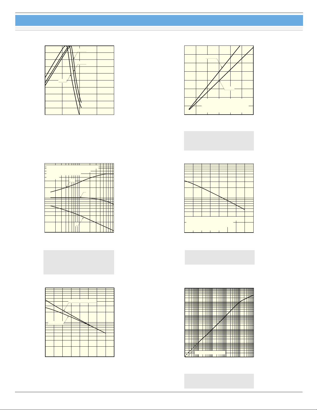
■ Spectral response
100
80
60
25 ˚C
40
RELATIVE VALUE (%)
20
0
1423 5
-20 ˚C
-10 ˚C
WAVELENGTH (µm)
■ S/N vs. chopping frequency
3
10
LIGHT SOURCE: BLACK BODY 500 K
INCIDENT ENERGY: 4.8 µW/cm
SUPPLY VOLTAGE: 15 V
tr: 200 µs
S/N
(Typ. Ta=25 ˚C)
2
(Typ.)
KIRDB0279EA
■ S/N vs. supply voltage
800
SIGNAL
600
400
SIGNAL (µV)
200
00
0
LIGHT SOURCE: BLACK BODY 500 K
INCIDENT ENERGY: 4.8 µW/cm
CHOPPING FREQUENCY: 600 Hz
FREQUENCY BANDWIDTH: 60 Hz
10 20
NOISE
30
(Typ. Ta=25 ˚C)
2
40 50 60
8
7
6
5
4
3
2
1
SUPPLY VOLTAGE (V)
If voltage of higher than 60 V is applied,
the noise increases exponentially, degrading the S/N. The device should be
operated at 60 V or less.
■ Photo sensitivity temperature characteristic
3
10
(Typ.)
NOISE (µV)
KIRDB0046EA
S
2
10
2
10
RELATIVE S/N
RELATIVE SENSITIVITY
LIGHT SOURCE: BLACK BODY 500 K
N
1
10
1
10
2
10
CHOPPING FREQUENCY (Hz)
Increasing the chopping frequency reduces the 1/f noise and results in an S/N
improvement. The S/N can also be im-
3
10
KIRDB0047EB
INCIDENT ENERGY: 4.8 µW/cm
CHOPPING FREQUENCY: 600 Hz
SUPPLY VOLTAGE: 15 V
1
10
-20
-100 102030405060
ELEMENT TEMPERATURE (˚C)
Cooling the device enhances its sensitivity, but the sensitivity also depends
on the load resistance in the circuit.
proved by narrowing the noise bandwidth
using a lock-in amplifier.
■ Dark resistance, rise time temperature characteristics ■ Photo sensitivity linearity
3
10
2
10
RISE TIME
RELATIVE VALUE
DARK RESISTANCE
(Typ.)
2
10
1
10
0
10
-1
10
RELATIVE OUTPUT
-2
10
(Typ. Ta=25 ˚C, FULLY ILLUMINATED)
2
KIRDB0048EB
1
10
-10 0 10 20 30 40 50 60-20
ELEMENT TEMPERATURE (˚C)
10
KIRDB0049EB
DEPENDENT ON NEP
-3
-9
10
10-810
INCIDENT ENERGY (W/cm2)
-7
-6
-5
10
10
-4
10
KIRDB0050EA
By making the incident light spot smaller
than the active area, the upper limit of
the linearity becomes lower.
2

PbS photoconductive detector
P2532-01, P2682-01
■ Cooling characteristics of TE-cooler ■ Current vs. voltage char acteristics of TE-cooler
(Typ. Ta=25 ˚C, Thermal resistance of heatsink=3 ˚C/W)
40
20
0
-20
TWO-STAGE
TE-COOLED
-40
ELEMENT TEMPERATURE (˚C)
-60
0 0.80.60.40.2 1.61.41.21.0
ONE-STAGE
TE-COOLED
CURRENT (A)
■ Thermistor temperature characteristic
6
10
5
10
(Typ.)
(Typ. Ta=25 ˚C, Thermal resistance of heatsink=3 ˚C/W)
1.6
1.4
1.2
1.0
0.8
0.6
CURRENT (A)
0.4
0.2
ONE-STAGE
TE-COOLED
TWO-STAGE
TE-COOLED
0
0 0.80.60.40.2 1.21.0
VOLTAGE (V)
KIRDB0171EA KIRDB0115EB
4
10
RESISTANCE (Ω)
3
10
-40 -30 0-20 2010-10 30
ELEMENT TEMPERATURE (˚C)
■ Connection example (P2682-01)
P2682-01
+
A3179-01
DETECTOR AND
C4696
CHOPPER
HEATSINK
BNC CONNECTOR CABLE
(SOLD SEPARATELY)
KIRDB0116EA
2-CONDUCTOR
SHIELDED CABLE
C3757-02
C1103-04
CABLE (SUPPLIED WITH C1103-04)
Connect C1103-04 and C3871
ground terminals together.
CABLE (SUPPLIED WITH C3757-02)
POWER SUPPLY FOR PREAMP
C3871
AMP
LOCK-IN AMP or
SPECTRUM ANALYZER
TEMPERATURE
CONTROLLER
SIGNAL
PROCESSING
CIRCUIT
KIRDC0003EA
3

■■
■
Dimensional outlines (unit: mm)
■■
PbS photoconductive detector
P2532-01, P2682-01
➀ P2532-01
PHOTOSENSITIVE
SURFACE
0.45
LEAD
5.1 ± 0.2
5.1 ± 0.2
15.3 ± 0.2
14 ± 0.2
WINDOW
10 ± 0.2
10.2 ± 0.2
6.4 ± 0.212 MIN.
4.5 ± 0.2
DETECTOR
DETECTOR
TE-COOLER (-)
TE-COOLER (+)
THERMISTOR
KIRDA0116EA
➁ P2682-01
PHOTOSENSITIVE
SURFACE
0.45
LEAD
5.1 ± 0.2
5.1 ± 0.2
15.3 ± 0.2
14 ± 0.2
WINDOW
10 ± 0.2
10 ± 0.212 MIN.
6.9 ± 0.2
10.2 ± 0.2
DETECTOR
DETECTOR
TE-COOLER (-)
TE-COOLER (+)
THERMISTOR
KIRDA0117EA
Information furnished by HAMAMATSU is believed to be reliable. However, no responsibility is assumed for possible inaccuracies or omissions.
HAMAMATSU PHOTONICS K.K., Solid State Division
1126-1 Ichino-cho, Hamamatsu City, 435-8558 Japan, Telephone: (81) 053-434-3311, Fax: (81) 053-434-5184, http://www.hamamatsu.com
U.S.A.: Hamamatsu Corporation: 360 Foothill Road, P.O.Box 6910, Bridgewater, N.J. 08807-0910, U.S.A., Telephone: (1) 908-231-0960, Fax: (1) 908-231-1218
Germany: Hamamatsu Photonics Deutschland GmbH: Arzbergerstr. 10, D-82211 Herrsching am Ammersee, Germany, Telephone: (49) 08152-3750, Fax: (49) 08152-2658
France: Hamamatsu Photonics France S.A.R.L.: 8, Rue du Saule Trapu, Parc du Moulin de Massy, 91882 Massy Cedex, France, Telephone: 33-(1) 69 53 71 00, Fax: 33-(1) 69 53 71 10
United Kingdom: Hamamatsu Photonics UK Limited: 2 Howard Court, 10 Tewin Road, Welwyn Garden City, Hertfordshire AL7 1BW, United Kingdom, Telephone: (44) 1707-294888, Fax: (44) 1707-325777
North Europe: Hamamatsu Photonics Norden AB: Smidesvägen 12, SE-171 41 Solna, Sweden, Telephone: (46) 8-509-031-00, Fax: (46) 8-509-031-01
Italy: Hamamatsu Photonics Italia S.R.L.: Strada della Moia, 1/E, 20020 Arese, (Milano), Italy, Telephone: (39) 02-935-81-733, Fax: (39) 02-935-81-741
Specifications are subject to change without notice. No patent rights are granted to any of the circuits described herein. ©2003 Hamamatsu Photonics K.K.
4
Cat. No. KIRD1019E06
Sep. 2003 DN
 Loading...