

Page 1

查询I1818A-08SR供应商
Production
March 2003
Features
®
Low Power Mobile VGA EMI Reduction IC
P1818/19/20/21/22
• FCC approved method of EMI attenuation
• Provides up to 15 dB EMI reduction
• Generates a low EMI spread spectrum clock and a
non-spread reference clock of the input frequency
• Optimized for frequency range from 10 MHz to 160
MHz
P1818: 10 to 20 MHz
P1819: 20 to 40 MHz
P1820: 40 to 80 MHz
P1821: 10 to 40 MHz
P1822: 80 to 160 MHz
• Internal loop filter minimizes external components
and board space
Product Description
The P18xx is a versatile spread spectrum frequency
modulator designed specifically for a wide range of input
clock frequencies from 10 to 160 MHz (see Input Frequency and Modulation Rate Selections). The P18xx
can generate an EMI reduced clock from crystal,
ceramic resonator, or system clock. The P18xx-A to
P18xx-H offer various combinations of spread options
and percentage deviations (see Spread Deviation Selections). These combinations include Down Spread,
Center Spread and percentage deviation range from
±0.625% to -3.50%.
The P18xx reduces electromagnetic interference (EMI)
at the clock source, allowing a system wide EMI
reduction for all the down stream clocks and data
dependent signals. The P18xx allows significant system
cost savings by reducing the number of circuit board
layers, ferrite beads, shielding, and other passive
components that are traditionally required to pass EMI
regulations.
• Selectable spread options: Down Spread and Center Spread
• Low inherent cycle-to-cycle jitter
• Eight spread % selections: +/-0.625% to –3.5%
• 3.3V operating voltage
• CMOS/TTL compatible inputs and outputs
• Low power CMOS design
• Supports notebook VGA and other LCD timing
controller applications
• Power down function for mobile application
• Products are available for industrial temperature
range.
• Available in 8-pin SOIC and TSSOP
The P18xx modulates the output of a single PLL in
order to “spread” the bandwidth of a synthesized clock,
thereby decreasing the peak amplitudes of its
harmonics. This results in significantly lower system
EMI compared to the typical narrow band signal
produced by oscillators and most clock generators.
Lowering EMI by increasing a signal’s bandwidth is
called “spread spectrum clock generation”.
The P18xx uses the most efficient and optimized
modulation profile approved by the FCC and is
implemented by using a proprietary all-digital method.
Applications
The P18xx is targeted toward EMI management for
memory and LVDS interfaces in mobile graphic
chipsets and high-speed digital applications such as
PC peripheral devices, consumer electronics , and
embedded controller systems.
Alliance Semiconductor
2575 Augustine Drive • Santa Clara, CA 95054 • Tel: 408.855.4900 • Fax: 408.855.4999 • www.alsc.com
Notice: The information in this document is subject to change without notice.
Page 2

Pin Diagrams
®
P1818/19/20/21/22
1 8
XIN
VSS
SRS
ModOut
2 7
3
4
XIN
VSS
D_C
ModOut
Block Diagram
P 1 8 1 8 A /B /C /D
P 1 8 1 9 A /B /C /D
P 1 8 2 0 A /B /C /D
1 8
2 7
3
P 1 8 1 8 E /F /G /H
4
P 1 8 1 9 E /F /G /H
P 1 8 2 0 E /F /G /H
6
5
6
5
XOUT
VDD
PD#
REF
XOUT
VDD
PD#
REF
VSS
SRS
ModOut
VSS
SRS
ModOut
1 8
XIN
2 7
3
4
P 1 8 2 1 A /B /C /D
1 8
XIN
2 7
3
4
P1822A
6
5
6
5
XOUT
VDD
FRS
REF
MRS
VDD
SSON#
SR0
XIN
XOUT
Crystal
Oscill a t o r
REF
Frequency
Divider
Feedback
Divider
D_C PD# MRS FRS SRS
Modulation
Phase
Detector
P1818/19/20/21/22 Block Diagram
Loop
Filter
VDD
VSS
PLL
VCO
Output
Divider
ModOUT
Low Power Mobile VGA EMI Reduction IC
Notice: The information in this document is subject to change without notice.
2 of 8March 2003
Page 3
Input Frequency and Modulation Rate
®
P1818/19/20/21/22
Part number
P1818 10 MHz to 20 MHz 10 MHz to 20 MHz Input frequency / 256
P1819 20 MHz to 40 MHz 20 MHz to 40 MHz Input frequency / 512
P1820 40 MHz to 80 MHz 40 MHz to 80 MHz Input frequency / 2048
FRS=0 10 MHz to 20 MHz 10 MHz to 20 MHz Input frequency / 256
P1821
FRS=1 20 MHz to 40 MHz 20 MHz to 40 MHz Input frequency / 512
P1822 80 MHz to 160 MHz 80 MHz to 160 MHz Input frequency / 3584
Spread Deviation Selections
Part number
2
P1818
/19/20/21A
P1818/19/20/21B 0 N/A N/A -1.25% (Down)
P1818/19/20/21C 0 N/A N/A +/-1.25% (Center)
P1818/19/20/21D 0 N/A N/A +/-0.625% (Center)
P1818/19/20E N/A N/A 0 -1.25% (Down)
P1818/19/20F N/A N/A 0 -2.5% (Down)
P1818/19/20G N/A N/A 0 -1.75% (Down)
2
P1818
P1822A
P1822B
1.A through H represents various combinations of spread deviations, options, and modulation rates.
2. Refer to Frequency vs. Deviation (P1818A and P1818H).
1
/19/20H
Input
frequency range
Output
frequency range
Modulation rate
SRS SR0 D_C Spread deviation
0 N/A N/A -2.50% (Down)
1 -3.50% (Down)
1 -1.75% (Down)
1 +/-1.75% (Center)
1 +/-0.875% (Center)
1 +/-0.625% (Center)
1 +/-1.25% (Center)
1 +/-0.875% (Center)
N/A N/A 0 -3.5% (Down)
1 +/-1.75% (Center)
0 0 N/A -1.25% (Down)
0 1 -2.50% (Down)
1 0 -1.75% (Down)
1 1 -3.50% (Down)
0 0 N/A +/-0.625% (Center)
0 1 +/-1.25% (Center)
1 0 +/-0.875% (Center)
1 1 +/-1.75% (Center)
Low Power Mobile VGA EMI Reduction IC
Notice: The information in this document is subject to change without notice.
3 of 8March 2003
Page 4

Frequency vs. Deviation (P1818A and P1818H)
Deviation in P1818A Deviation in P181 8H
Frequency
SRS = 1 SRS = 0 D_C = 1 D_C = 0
10 MHz -4.4% -3.3% -4.4% ±2.2%
15 MHz -1.8% -1.26% -1.8% ±0.9%
20 MHz -0.8% -0.6% -0.8% ±0.4%
Pin Description
®
P1818/19/20/21/22
Pin
number
Name Type Description
1 XIN I Connect to externally generated clock signal or crystal.
2 VSS P Ground Connection. Connect to system ground.
3 SRS I Spread Range Select. Digital logic input used to select frequency devi-
ation (see Spread Deviation Selections). This pin has an internal pullup resistor.
1
3
D_C I Digital logic input used to select Down (LOW) or Center (HIGH) Spread
Options (see Spread Deviation Selections). This pin has an internal
pull-up resistor.
4 ModOut O Spread Spectrum clock output (see Input Frequency and Modulation
Rate Selections and Spread Deviation Selections).
5 REF O Non-modulated reference output clock of the input frequency.
5/6
1
FRS I Frequency Range Select. Digital logic input used to select input fre-
quency range (see Input Frequency and Modulation Rate Selections).
This pin has an internal pull-up resistor.
1
6
PD# I Power-Down control pin. Pull LOW to enable Power-Down mode. This
pin has an internal pull-up resistor.
7 VDD P Connect to +3.3V
8 XOUT I Connect to crystal. No connect if externally generated clock signal is
used.
1
8
MRS I Modulation Rate Select. Digital logic input used to select Modulation
Rate (see Spread Deviation Selections). This pin has an internal pull-
up resistor.
1. Please refer to Figure 1 for pin assignment.
Low Power Mobile VGA EMI Reduction IC
Notice: The information in this document is subject to change without notice.
4 of 8March 2003
Page 5

Absolute Maximum Ratings
Symbol Parameter Rating Unit
®
P1818/19/20/21/22
, V
V
DD
T
STG
T
A
Voltage on any pin with respect to GND -0.5 to +7.0 V
IN
Storage temperature -65 to +125 º C
Operating temperature 0 to +70 º C
DC Electrical Characteristics
3.3 V, 25° C
Symbol Parameter Min Typ Max Unit
V
V
I
I
I
XOL
I
XOH
IL
IH
IL
IH
Input low voltage GND – 0.3 – 0.8 V
Input high voltage 2.00 – V
Input low current (inputs D_C,
-60.0 – -20.00 µA
+ 0.3 V
DD
PD#, MRS, FRS, SRS)
Input high current – – 1.00 µA
XOUT output low current
(@ 0.4 V, V
= 3.3 V)
DD
XOUT output high current
(@ 2.5 V, V
= 3.3 V)
DD
2.00 – 12.00 mA
––12.00mA
V
Z
V
I
DD
I
CC
V
t
ON
OUT
OL
OH
DD
Output low voltage
(V
=3.3 V, IOL = 20 mA)
DD
Output high voltage
(V
=3.3 V, IOH = 20 mA)
DD
Static supply current
––0.4V
––2.8V
–4.5–mA
Standby mode
Dynamic supply current
Normal mode (3.3 V and 25 pF
7.1
f
IN-min
–26.9
f
IN-max
probe loading)
Operating voltage – 3.3 – V
Power up time
–0.18– mS
(first locked clock cycle after
power up)
Clock output impedance – 50 – Ω
mA
Low Power Mobile VGA EMI Reduction IC
Notice: The information in this document is subject to change without notice.
5 of 8March 2003
Page 6

®
AC Electrical Characteristics
3.3 V, 25° C
Symbol Parameter Min Typ Max Unit
P1818/19/20/21/22
Input frequency 10 – 160 MHz
Output frequency 10 – 160 MHz
Output rise time
(measured at 0.8 V to 2.0 V)
Output fall time
(measured at 2.0 V to 0.8 V)
Jitter (cycle to cycle) at 20 MHz -200 – 200 ps
Output duty cycle 45 50 55 %
and tHL are measured into a capacitive load of 15 pF
f
t
t
1. t
f
IN
OUT
LH
HL
t
JC
t
D
LH
1
1
–0.66– ns
–0.65– ns
Low Power Mobile VGA EMI Reduction IC
Notice: The information in this document is subject to change without notice.
6 of 8March 2003
Page 7

Mechanical Package Outline (8-Pin SOIC)
C
®
P1818/19/20/21/22
Inches Millimeters
Symbol
Min Nor Max Min Nor Max
L
P18xxx
LOT NUMBER
YYWW
D
eB
H
A
A2
A1
E
a
Mechanical Package Outline (8-Pin TSSOP)
C
A 0.057 0.064 0.071 1.45 1.63 1.80
A1 0.004 0.007 0.010 0.10 0.18 0.25
A2 0.053 0.061 0.069 1.35 1.55 1.75
B 0.012 0.016 0.020 0.31 0.41 0.51
C 0.004 0.006 0.01 0.10 0.15 0.25
D 0.186 0.194 0.202 4.72 4.92 5.12
E 0.148 0.156 0.164 3.75 3.95 4.15
e 0.050 BSC 1.27 BSC
H 0.224 0.236 0.248 5.70 6.00 6.30
L 0.012 0.020 0.028 0.30 0.50 0.70
a 0°5°8°0°5°8°
Note: Controlling dimensions are millimeters.
SOIC: 0.074 grams unit weight.
Inches Millimeters
Symbol
Min Nor Max Min Nor Max
L
A – – 0.047 – – 1.10
A1 0.002 – 0.006 0.05 – 0.15
P
18xxx
Lot #
H
YYWW
E
A2 0.031 0.039 0.041 0.80 1.00 1.05
B 0.007 – 0.012 0.19 – 0.30
C 0.004 – 0.008 0.09 – 0.20
a
D
D 0.114 0.118 0.122 2.90 3.00 3.10
E 0.169 0.173 0.177 4.30 4.40 4.50
A
A2
e 0.026 BSC 0.65 BSC
H 0.244 0.252 0.260 6.20 6.40 6.60
eB
A1
L 0.018 0.024 0.030 0.45 0.60 0.75
a 0° – 8° 0° – 8°
Note: Controlling dimensions are millimeters.
TSSOP: 0.034 grams unit weight.
Low Power Mobile VGA EMI Reduction IC
Notice: The information in this document is subject to change without notice.
7 of 8March 2003
Page 8

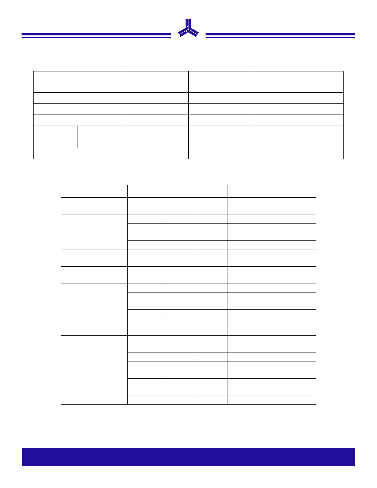
Ordering Information
X18XXX -08 XX
12345
1. Flow prefix:
I = industrial temperature range (-40° C to 85° C)
P = commercial temperature range (0° C to 70° C)
2. Device number
3. Deviation (%) and spread option identifier
4. Device pin count
5. Package identifier:
ST = SOIC in tube
SR = SOIC in tape and reel
TT = TSSOP in tube
TR = TSSOP in tape and reel
®
P1818/19/20/21/22
Example:
Ordering
number
Marking
Input
frequency
(MHz)
P1818A-08ST P1818A 10 – 20 -2.5, -3.5 8 PIN SOIC, TUBE 0°C to 70°C
P1818A-08SR P1818A 10 – 20 -2.5, -3.5 8 PIN SOIC, TAPE &
P1818A-08TT P1818A 10 – 20 -2.5, -3.5 8 PIN TSSOP, TUBE 0°C to 70°C
P1818A-08TR P1818A 10 – 20 -2.5, -3.5 8 PIN TSSOP, TAPE &
1. Products are available for industrial temperature range operation. Please contact factory for more information.
Licensed under U.S. patent numbers 5,488,627 and 5,631,920.
Frequency
deviation
(%)
Package
type
REEL
REEL
Qty . /
reel
Temp
2,500 0°C to 70°C
2,500 0°C to 70°C
1
© Copyright 2003 Alliance Semiconductor Corporation. All rights reserved. Our three-point logo, our name and Intelliwatt are trademarks or registered trademarks of Alliance. All other brand and product
names may be the trademarks of their respective companies. Alliance reserves the right to make changes to this document and its products at any time without notice. Alliance assumes no responsibility
for any errors that may appear in this document. The data contained herein represents Alliance's best data and/or estimates at the time of issuance. Alliance reserves the right to change or correct this
data at any time, without notice. If the product described herein is under development, significant changes to these specifications are possible. The information in this product data sheet is intended to
be general descriptive information for potential customers and users, and is not intended to operate as, or provide, any guarantee or warrantee to any user or customer. Alliance does not assume any
responsibility or liability arising out of the application or use of any product described herein, and disclaims any express or implied warranties related to the sale and/or use of Alliance products including
liability or warranties related to fitness for a particular purpose, merchantability, or infringement of any intellectual property rights, except as express agreed to in Alliance's Terms and Conditions of Sale
(which are available from Alliance). All sales of Alliance products are made exclusively according to Alliance's Terms and Conditions of Sale. The purchase of products from Alliance does not convey a
license under any patent rights, copyrights, mask works rights, trademarks, or any other intellectual property rights of Alliance or third parties. Alliance does not authorize its products for use as critical
components in life-supporting systems where a malfunction or failure may reasonably be expected to result in significant injury to the user, and the inclusion of Alliance products in such life-supporting
systems implies that the manufacturer assumes all risk of such use and agrees to indemnify Alliance against all claims arising from such use.
Low Power Mobile VGA EMI Reduction IC
Notice: The information in this document is subject to change without notice.
8 of 8March 2003
 Loading...