

Page 1

Data Sheet
March 2000
ORCA
®
OR3LP26B Field-Programmable System Chip (FPSC
)
Embedded Master/Target PCI Interface
Introduction
Lucent Technologies Microelectronics Group has
developed a solution for designers who need the
many advantages of an FPGA-based design implementation, coupled with the high bandwidth of an
industry-standard PCI interface. The
ORCA
OR3LP26B (a member of the Series 3+ FPSC family)
provides a full-featured 33/50/66 MHz, 32-/64-bit PCI
interface, fully designed and tested, in hardware, plus
FPGA logic for user-programmable functions.
PCI Bus Core Highlights
■
Implemented in an
ORCA
Series 3 OR3L125B
base array, displacing the bottom ten rows of 28
columns.
■
Core is a well-tested ASIC model.
■
Fully compliant to Revision 2.2 of PCI Local Bus
specification.
■
Operates at PCI bus speeds up to 66 MHz on a
32-/64-bit wide bus.
■
Comprises two independent controllers for Master
and Target.
■
Meets/exceeds all requirements for
PICMG
*
Hot
Swap friendly silicon, full Hot Swap model, per the
CompactPCI
*
Hot Swap specification,
PICMG
2.1
R1.0.
■
PCI SIG Hot Plug (R1.0) compliant.
■
Four internal FIFOs individually buffer both directions of both the Master and Target interfaces:
— Both Master FIFOs are 64 bits wide by 32 bits
deep.
— Both Target FIFOs are 64 bits wide by 16 bits
deep.
■
Capable of no-wait-state, full-burst PCI transfers in
either direction, on either the Master or Target
interface. The dual 64-bit data paths extend into
the FPGA logic, permitting full-bandwidth, simultaneous bidirectional data transfers of up to
528 Mbytes/s to be sustained indefinitely.
■
Can be configured to provide either two 64-bit
buses (one in each direction) to be multiplexed
between Master and Target, or four independent
32-bit buses.
■
Provides many hardware options in the PCI core
that are set during FPGA logic configuration.
■
Operates within the requirements of the PCI 5 V
and 3.3 V signaling environments and 3.3 V commercial environmental conditions, allowing the
same device to be used in 5 V or 3.3 V PCI systems.
■
FPGA is reconfigurable via the PCI interface's configuration space (as well as conventionally), allowing the FPGA to be field-updated to meet latebreaking requirements of emerging protocols.
*
PICMG
and
CompactPCI
are registered trademarks of the PCI
Industrial Computer Manufacturers Group.
Table 1.
ORCA
OR3LP26B PCI FPSC Solution—Available FPGA Logic
†The embedded core and interface comprise approximately 85K standard-cell ASIC gates in addition to these usable gates. The usable
gate counts range from a logic-only gate count to a gate count assuming 30% of the PFUs/SLICs being used as RAMs. The logic-only
gate count includes each PFU/SLIC (counted as 108 gates per PFU/SLIC), including 12 gates per LUT/FF pair (eight per PFU), and 12
gates per SLIC/FF pair (one per PFU). Each of the four PIOs per PIC is counted as 16 gates (two FFs, fast-capture latch, output logic,
CLK drivers, and I/O buffers). PFUs used as RAM are counted at four gates per bit, with each PFU capable of implementing a 32 x 4
RAM (or 512 gates) per PFU.
Device Usable Gates
†
Number of
LUTs
Number of
Registers
Max User
RAM
Max User
I/Os
Array
Size
Number of
PFUs
OR3LP26B 60K—120K 4032 5304 64K 259 18 x 28 504
Page 2

Table of Contents
Contents Page Contents Page
ORCA
OR3LP26B FPSC Data Sheet
Embedded Master/Target PCI Interface March 2000
2 Lucent Technologies Inc.
Introduction ..........................................................................1
PCI Bus Core Highlights ......................................................1
Figures .................................................................................2
Tables ..................................................................................3
FPSC Highlights ...................................................................5
Software Support .................................................................6
Description ...........................................................................7
What Is an FPSC? ............................... ...... ...... ..... ...... ......7
FPSC Overview .......................................... ...... ..... ...... ......7
FPSC Gate Counting ........................................................7
FPGA/Embedded Core Interface ......................................7
ORCA
Foundry Development System ..............................7
FPSC Design Kit ...............................................................8
FPGA Logic Overview .......................................................8
PLC Logic ..........................................................................8
PIC Logic .............................................. .............................9
System Features ...............................................................9
Routing ..............................................................................9
Configuration .....................................................................9
Boundary Scan ..................................................................9
More Series 3 Information .................................................9
OR3LP26B Overview .........................................................10
Device Layout ............................................................. ....10
PCI Local Bus ................................. ..... ...........................10
OR3LP26B PCI Bus Core Overview ...............................12
PCI Bus Interface ............................................................12
Embedded Core Options/FPGA Configuration ...............13
PCI Bus Core Detailed Description ....................................14
PCI Bus Commands .............................................. ...... ....14
PCI Protocol Fundamentals ............................. ...............16
FIFO Memories and Control ............................................17
PCI Bus Pin Information ............................. .....................18
PCI Bus Core Detailed Description Dual Port ....................21
Embedded Core/FPGA Interface Signal Descriptions ....21
Embedded Core/FPGA Interface Signal Locations .........27
Embedded Core Bit Stream Configurable Options .........32
Understanding FIFO Packing/Unpacking ........................33
Embedded Core/FPGA Interface Operation ...................34
Embedded Core/FPGA Interface Operation Summary ...35
Master (FPGA Initiated) Write .........................................36
Master (FPGA Initiated) Read .........................................42
Target (PCI Bus Initiated) Write ......................................49
Target (PCI Bus Initiated) Read ......................................58
PCI Bus Core Detailed Description Quad Port ...................70
Embedded Core/FPGA Interface Signal Descriptions ....70
Embedded Core/FPGA Interface Signal Locations .........76
Embedded Core Bit Stream Configurable Options .........83
Understanding FIFO Packing/Unpacking ........................84
Embedded Core/FPGA Interface Operation ...................86
Embedded Core/FPGA Interface Operation Summary ...87
Master (FPGA Initiated) Write .........................................88
Master (FPGA Initiated) Read .........................................94
Target (PCI Bus Initiated) Write ....................................101
Target (PCI Bus Initiated) Read ....................................110
Configuration Space of the PCI Core ...............................123
PCI Bus Configuration Space Organization ..................123
FPSC Configuration ................................... ...... ..... ...... .....126
Configuration via PCI Bus .............................................126
Readback via PCI interface ..........................................127
Interaction Among Configurat io n Modes ......................127
Clocking Options at FPGA/Core Boundary ..................... 128
PCI Clock as System Clock ..........................................128
Local Clock as System Clock .......................................128
FPGA Configuration Data Format ...................................130
Using
ORCA
Foundry to Generate Configuration
RAM Data ...................................................................130
FPGA Configuration Data Frame ..................................130
Bit Stream Error Checking ...............................................132
FPGA Configuration Modes .............................................132
Powerup Sequencing for Series OR3LP26B Device .......133
Absolute Maximum Ratings .............................................133
Recommended Operating Conditi ons .............................134
Electrical Characteristics .................................................135
Timing Characteristics .....................................................136
Description ....................................................................136
Clock Timing .................................................................137
Input/Output Buffer Measurement Conditions ................. 148
Output Buffer Characteristics ..........................................149
Estimating Power Dissipation ..........................................150
Pin Information ................................................................151
Package Compatibility ..................................................154
Package Thermal Characteristics Summary ................... 178
Θ
JA ............................................................................... 178
ψ
JC ............................................................................... 178
Θ
JC ...............................................................................178
Θ
JB ............................................................................... 178
FPGA Maximum Junction Temperature .......................178
Package Coplanarity .......................................................179
Package Parasitics ..........................................................180
Package Outline Diagrams ..............................................181
Terms and Definitions ...................................................181
352-Pin PBGA ..............................................................182
680-Pin PBGA ..............................................................183
Ordering Information ........................................................184
Figures
Figure 1. ORCA OR3LP26B PCI FPSC
Block Diagram...............................................................13
Figure 2. Master Write Single (FPGA Bus, Dual-Port).....38
Figure 3. Master Write Single (PCI Bus, 64-Bit)..............39
Figure 4. Master Write 32-Byte Burst
(FPGA Bus, Dual-Port) .................................................40
Figure 5. Master Write 32-Byte Burst (PCI Bus, 64-Bit)..41
Figure 6. Master Read Single (FPGA Bus, Dual-Port,
Specified Burst Length, 64-Bit Address).......................44
Figure 7. Master Read Single (PCI Bus, 64-Bit)..............45
Figure 8. Master Read 32-Byte Burst (FPGA Bus,
Dual-Port, Burst Length, and 64-Bit Address)..............46
Figure 9. Master Read 32-Byte Burst
(PCI Bus, 64-Bit)...........................................................47
Page 3

Lucent Technologies Inc. 3
Lucent Technologies Inc.
Table of
Contents
(continued)
Contents Page Contents Page
Data Sheet
ORCA
OR3LP26B FPSC
Marc h 2000 Embedded Master/Target PCI Inte rface
Figure 10. Target Configuration Write
(PCI Bus, 64-Bit)...........................................................52
Figure 11. Target I/O Write, Delayed (PCI Bus, 64-Bit) ...53
Figure 12. Target Write Memory Single
(PCI Bus, 64-Bit)...........................................................54
Figure 13. Target Write Single (FPGA Bus, Dual-Port)....55
Figure 14. Target Memory Write 32-Byte Burst
(PCI Bus, 64-Bit)...........................................................56
Figure 15. Target Write Memory 32-Byte Burst
(FPGA Bus, Dual-Port) ....................................... ...... ....57
Figure 16. Target Configuration Read
(PCI Bus, 64-Bit)...........................................................61
Figure 17. Target I/O Read, Delayed (PCI Bus, 64-Bit)...62
Figure 18. Target I/O Read, Not Delayed
(PCI Bus, 64-Bit)...........................................................63
Figure 19. Target Memory Single Read, Delayed
(PCI Bus, 64-Bit)...........................................................64
Figure 20. Target Read Single (FPGA Bus, Dual-Port)....65
Figure 21. Target Memory Read Single, Not Delayed
(PCI Bus, 64-Bit)...........................................................66
Figure 22. Target Memory Read 32-Byte Burst, Delayed
(PCI Bus, 64-Bit)...........................................................67
Figure 23. Target Read Memory 32-Byte Burst
(FPGA, Dual-Port) ........................................................68
Figure 24. Target Read Memory Burst, No Delayed
(PCI Bus, 32-Bit)...........................................................69
Figure 25. Master Write Single (PCI Bus, 64-Bit)............90
Figure 26. Master Write 32-Byte Burst
(PCI Bus, 64-Bit)...........................................................91
Figure 27. Master Write Single Quadword
(FPGA Bus, Quad-Port, 64-Bit Address)......................92
Figure 28. Master Write 32-Byte Burst
(FPGA Bus, Quad-Port, 64-Bit Address)......................93
Figure 29. Master Read Single (PCI Bus, 64-Bit)............96
Figure 30. Master Read Single Quadword (FPGA Bus,
Quad-Port, Specified Burst Length, 32-Bit Address) ....97
Figure 31. Master Read 32-Byte Burst
(PCI Bus, 64-Bit)...........................................................98
Figure 32. Master Read 32-Byte Burst (FPGA Bus,
Quad-Port, Specified Burst Length, 32-Bit Address) ....99
Figure 33. Target Configuration Write
(PCI Bus, 64-Bit)...........................................................104
Figure 34. Target I/O Write, Delayed (PCI Bus, 64-Bit) ...105
Figure 35. Target Write Memory Single
(PCI Bus, 64-Bit)...........................................................106
Figure 36. Target Write Single Quadword
(FPGA Bus, Quad-Port, 64-Bit Address)......................107
Figure 37. Target Memory Write 32-Byte Burst
(PCI Bus, 64-Bit)...........................................................108
Figure 38. Target Write Memory 32-Byte Burst
(FPGA Bus, Quad-Port, 32-Bit Address)......................109
Figure 39. Target Configuration Read
(PCI Bus, 64-Bit)...........................................................113
Figure 40. Target I/O Read, Delayed
(PCI Bus, 64-Bit)...........................................................114
Figure 41. Target I/O Read, Not Delayed
(PCI Bus, 64-Bit) ......................................................... .115
Figure 42. Target Memory Single Read, Delayed
(PCI Bus, 64-Bit) ......................................................... .116
Figure 43. Target Read Single (FPGA Bus, Quad-Port,
64-Bit Address).............................................................1 17
Figure 44. Target Memory Read Single, Not Delayed
(PCI Bus, 64-Bit) ......................................................... .118
Figure 45. Target Memory Read 32-Byte Burst, Delayed
(PCI Bus, 64-Bit) ......................................................... .119
Figure 46. Target Read Memory 32-Byte Burst
(FPGA Bus, Quad-Port, 32-Bit Address)......................120
Figure 47. Target Read Memory Burst, No Delayed
(PCI Bus, 32-Bit) ......................................................... .121
Figure 48. FPSC Block Diagram and Clock Network......129
Figure 49. Serial Configuration Data Format—
Autoincrement Mode....................................................131
Figure 50. Serial Configuration Data Format—
Explicit Mode................................................................131
Figure 51. ExpressCLK to Output Delay.........................138
Figure 52. Fast Clock to Output Delay ............................139
Figure 53. System Clock to Output Delay.......................140
Figure 54. Input to ExpressCLK Setup/Hold Time..........141
Figure 55. Input to Fast Clock Setup/Hold Time..............142
Figure 56. Input to System Clock Setup/Hold Time........143
Figure 57. ac Test Loads.................................................148
Figure 58. Output Buffer Delays......................................148
Figure 59. Input Buffer Delays.........................................148
Figure 60. Sinklim (TJ = 25 °C, VDD = 3.3 V).................149
Figure 61. Slewlim (TJ = 25 °C, VDD = 3.3 V)................149
Figure 62. Fast (TJ = 25 °C, VDD = 3.3 V)......................149
Figure 63. Sinklim (TJ = 125 °C, VDD = 3.0 V)...............149
Figure 64. Slewlim (TJ = 125 °C, VDD = 3.0 V)..............149
Figure 65. Fast (TJ = 125 °C, VDD = 3.0 V)....................149
Figure 66. Package Parasitics.........................................180
Tables
Table 1. ORCA OR3LP26B PCI FPSC Solution—
Available FPGA Logic...................................................1
Table 2. PCI Local Bus Data Rates................................10
Table 3. OR3LP26B Array..............................................11
Table 4. PCI Bus Command Descriptions......................14
Table 5. Timing Budgets.................................................17
Table 6. FIFO Flags Provided to FPGA Application.......18
Table 7. PCI Bus Pin Descriptions..................................18
Table 8. Embedded Core/FPGA Interface Signals.........21
Table 9. OR3LP26B FPGA/PCI Core Interface Signal
Locations......................................................................27
Table 10. Bit Definitions on FPGA/PCI Core Interface...30
Table 11. Address Cycle Sequences for Various
Operations ................................................................... 31
Table 12. PCI Core Options Settable via FPGA
Configuration RAM Bits................................................32
Page 4

Table of
Contents
(continued)
Contents Page Contents Page
ORCA
OR3LP26B FPSC Data Sheet
Embedded Master/Target PCI Interface March 2000
4 Lucent Technologies Inc.
Table 13. Dual-Port FIFO Packing/Unpacking, Case 1,
PCI Side ........................................................... ..... ......33
Table 14. Dual-Port FIFO Packing/Unpacking, Case 1,
FPGA Side ..................................................................33
Table 15. Dual-Port FIFO Packing/Unpacking, Case 2,
PCI Side...................................................... ...... ..... ......33
Table 16. Dual-Port FIFO Packing/Unpacking, Case 2,
FPGA Side ..................................................................34
Table 17. Index to State Sequence Tables.....................35
Table 18. Dual-Port Master Write ..................................41
Table 19. Dual-Port Master Read, 64-Bit Address
Supplied.......................................................................48
Table 20. Dual-Port Master Read, 32-Bit Address
Supplied ...................................................................... 48
Table 21. Dual-Port Target Write ...................................57
Table 22. Dual-Port Target Read ...................................69
Table 23. Embedded Core/FPGA Interface Signals....... 70
Table 24. OR3LP26B FPGA/PCI Core Interface Signal
Locations......................................................................76
Table 25. Bit Definitions on FPGA/PCI Core Interface...79
Table 26. Address Cycle S equences for Various
Operations ...................................................................82
Table 27. PCI Core Options Settable via FPGA
Configuration RAM Bits................................................83
Table 28. Quad-Port FIFO Packing/Unpacking, Case 1,
PCI Side...................................................... ...... ..... ......84
Table 29. Dual-Port FIFO Packing/Unpacking, Case 1,
FPGA Side ..................................................................84
Table 30. Quad-Port FIFO Packing/Unpacking, Case 1,
PCI Side ........................................................... ..... ......85
Table 31. Quad-Port FIFO Packing/Unpacking,
Case 1, FPGA Side......................................................85
Table 32. Quad-Port FIFO Packing/Unpacking, Case 2,
PCI Side...................................................... ...... ..... ......85
Table 33. Quad-Port FIFO Packing/Unpacking, Case 1,
FPGA Side...................................................................85
Table 34. Holding Registers, Examples of Typical
Operation .....................................................................86
Table 35. Index to State Sequence Tables.....................87
Table 36. Quad-Port Master Write .................................93
Table 37. Quad-Port Master Read, Duplicate Burst
Length and 16-Bit Address...........................................100
Table 38. Quad-Port Master Read, Specified Burst
Length and 64-Bit Address ..........................................100
Table 39. Quad-Port Target Write ..................................109
Table 40. Quad-Port Target Read...................................122
Table 41. Configuration Space Layout............................123
Table 42. Configuration Space Assignment ................... 124
Table 43. Configuration Frame Format and Contents .... 131
Table 44. Configuration Frame Size...............................132
Table 45. Configuration Modes.......................................132
Table 46. Absolute Maximum Ratings............................133
Table 47. Recommended Operating Conditions.............134
Table 48. Electrical Characteristics................................135
Table 49. Derating for Commercial Devices
(I/O Supply VDD) ............................. ..... ...... ...... ...........136
Table 50. .........................................................................Der-
ating for Commercial Devices (I/O Supply VDD2)........136
Table 51. ExpressCLK (ECLK) and Fast Clock (fclk)
TimingCharacteristics...................................................137
Table 52. General-Purpose Clock Timing
Characteristics (Internally Generated Clock)................138
Table 53. OR3LP26B ExpressCLK to Output
Delay (Pin-to-Pin)............................................... ...... ....138
Table 54. OR3LP26B Fast Clock (fclk) to Output
Delay (Pin-to-Pin)............................................... ...... ....139
Table 55. OR3LP26B General System Clock (SCLK)
to Output Delay (Pin-to-Pin)..........................................140
Table 56. OR3LP26B Input to ExpressCLK (ECLK)
Fast-Capture Setup/Hold Time (Pin-to-Pin)..................141
Table 57. OR3LP26B Input to Fast Clock
Setup/Hold Time (Pin-to-Pin)........................................142
Table 58. OR3LP26B Input to General System
Clock (SCLK) Setup/Hold Time (Pin-to-Pin).................143
Table 59. OR3LP26B PCI and FPGA Interface Clock
Operation Frequencies.................................................143
Table 60. OR3LP26B FPGA to PCI, and PCI to FPGA,
Combinatorial Path Delays...........................................144
Table 61. OR3LP26B FPGA Side Interface
Combinatorial Path Delay Signals ................................144
Table 62. OR3LP26B Interbuf Delays.............................145
Table 63. OR3LP26B FPGA Side Interface Clock to
Output Delays, pciclk Synchronous Signals.................145
Table 64. OR3LP26B FPGA Side Interface Clock to
Output Delays, fclk Synchronous Signals.....................146
Table 65. OR3LP26B FPGA Side Interface Input
Setup Delays, pciclk Synchronous Signals...................147
Table 66. OR3LP26B FPGA Side Interface Input
Setup Delays, fclk Synchronous Signals ......................147
Table 67. PCI Core Internal Power Dissapation .............150
Table 68. FPGA Common-Function Pin Descriptions.....151
Table 69. ORCA OR3LP26B I/Os Summary ..................154
Table 70. Pinout Information ..........................................155
Table 71. ORCA OR3LP26B Plastic Package Thermal
Guidelines.....................................................................178
Table 72. Package Coplanarity.......................................179
Table 73. Package Parasitics..........................................180
Table 74. Voltage Options...............................................184
Table 75. Package Options.............................................184
Table 76. ORCA Series 3+ Package Matrix....................184
Table 77. Embedded Core Type......................................184
Table 78. FPSC Base Array............................................184
Page 5

Lucent Technologies Inc. 5
Data Sheet
ORCA
OR3LP26B FPSC
Marc h 2000 Embedded Master/Target PCI Inte rface
Lucent Technologies Inc.
PCI Bus Core Highlights
(continued)
■
Master:
— Generates all defined command codes except
interrupt acknowledge and special cycle.
— Capable of accessing its own local Target.
— Capable of acting as the system's configuration
agent by booting up with the Master logic
enabled.
— Supports multiple options for Master bus requests,
to increase PCI bus bandwidth.
— Supports single-cycle I/O space accesses.
— Provides option to delay PCI access until FIFO is
full on Master writes to increase PCI bandwidth.
— Supports programmable latency timer control.
■
Target:
— Responds legally to all command codes: interrupt
acknowledge, special cycle, and reserved com-
mands ignored; memory read multiple and line
handled as memory read; memory write and
invalidate handled as memory write.
— Implements Target abort, disconnect, retry, and
wait cycles.
— Handles delayed transactions.
— Handles fast back-to-back transactions.
— Method of handling retries is programmable at
FPGA configuration to allow tailoring to different
Target data access latencies.
— Decodes at medium speed.
— Provides option to delay PCI access until FIFO is
full on Target reads to increase PCI bandwidth.
■
Supports dual-address cycles (both as Master and
Target).
■
Supports all six base address registers (BARs), as
either memory (32-bit or 64-bit) or I/O. Any legal
page size can be independently specified for each
BAR during FPGA configuration.
■
Independent Master and Target clocks can be supplied to the PCI FIFO interface from the FPGA-based
logic.
■
Provides vers atile clocking capabilities with FPGA
clocks sourced from PCI bus clock or elsewhere.
FIFO interface buffers asynchronous clock domains
between the PCI interface and FPGA-based logic.
■
PCI interface timing: meets or exceeds 33 MHz,
50 MHz, and 66 MHz PCI requirements.
■
Configuration options:
— Class code, revision ID.
— Latency timer.
— Cache line size.
— Subsystem ID.
— Subsystem vendor ID.
— Maximum latency, minimum grant.
— Interrupt line.
— Hot Plug/Hot Swap capability.
■
Generates interrupts on
intan
as directed by the
FPGA.
■
PCI I/O output drivers can be programmed for fast or
slew-limited operation.
■
Automatically detects 5 V or 3.3 V PCI bus signaling
environment and provides appropriate I/O signaling,
under 3.3 V commercial conditions.
■
Ideally suited for such applications as:
— PCI-based graphics/video/multimedia.
— Bridges to ISA/EISA/MCA, LAN, SCSI, Ethernet,
ATM, or other bus architectures.
— High-bandwidth data transfer in proprietary sys-
tems.
FPSC Highlights
■
Implemented as an embedded core into the
advanced Series 3+
ORCA
FPSC architecture.
■
Allows the user to integrate the core with up to 120K
gates of programmable logic, all in one device, and
provides up to 259 user I/O pins in addition to the
PCI interface pins.
■
FPGA portion retains all of the features of the
ORCA
3 FPGA architecture:
— High-performance, cost-effective, 0.25 µm
5-level metal technology.
— Twin-quad programmable function unit (PFU)
architecture with eight 16-bit look-up tables
(LUTs) per PFU, organized in two nibbles for use
in nibble- or byte-wide functions. Allows for mixed
arithmetic and logic functions in a single PFU.
Parameter 33 MHz 50 MHz 66 MHz
Device Clock = > Out 11.0 ns 7.5 ns 6.0 ns
Device Setup Time 7.0 ns 4.5 ns 3.0 ns
Board Prop. Delay 10.0 ns 6.5 ns 5.0 ns
Board Clock Skew 2.0 ns 1.5 ns 1.0 ns
Total Budget 30.0 ns 20.0 ns 15.0 ns
Load Capacitance 50 pF 50 pF 10 pF
Page 6

66 Lucent Technologies Inc.
ORCA
OR3LP26B FPSC Data Sheet
Embedded Master/Target PCI Interface March 2000
Lucent Technologies Inc.
FPSC Highlights
(continued)
— Softwired LUTs (SWL) allow fast cascading of up
to three levels of LUT logic in a single PFU.
— Supplemental logic and interconnect cell (SLIC)
provides 3-statable buffers, up to 10-bit decoder,
and
PAL
*-like AND-OR-INVERT (AOI) in each
programmable logic cell (PLC).
— Up to three ExpressCLK inputs allow extremely
fast clocking of signals on- and off-chip plus
access to internal general clock routing.
— Dual-use microprocessor interface (MPI) can be
used for configuration, readback, device control,
and device status, as well as for a general-purpose interface to the FPGA. Glueless interface to
i960
†
and
PowerPC
‡ processors w ith use r-co nf ig-
urable address space provided.
— Programmable clock manager (PCM) adjusts
clock phase and duty cycle for input clock rates
from 5 MHz to 120 MHz. The PCM may be combined with FPGA logic to create complex functions, such as digital phase-locked loops (DPLL),
frequency counters, and frequency synthesizers
or clock doublers. Two PCMs are provided per
device.
— True internal 3-state, bidirectional buses with sim-
ple control provided by the SLIC.
— 32 x 4 RAM per PFU, configurable as single or
dual port. Create large, fast RAM/ROM blocks
(128 x 8 in only eight PFUs) using the SLIC
decoders as bank drivers.
— Built-in boundary scan (
IEEE
§
1149.1 JTAG) and
TS_ALL testability function to 3-state all I/O pins.
■
High-speed on-chip interface provided between
FPGA logic and embedded core to reduce bottlenecks typically found when interfacing off-chip.
■
Supported in two packages: 352-pin PBGA and
680-pin PBGAM.
*
PAL
is a trademark of Advanced Micro Devices, Inc.
†
i960
is a registered trademark of Intel Corporation.
‡
PowerPC
is a registered trademark of International Business
Machines Corporation.
§
IEEE
is a registered trademark of The Institute of Electrical and
Electronics Engineers, Inc.
Note
: This document will conform to the nomenclature
of the PCI Local Bus Specification, as follows:
Software Support
■
Supported by
ORCA
Foundry software and third-
part
y
CAE tools for implementing
ORCA
Series 3+
devices and simulation/timin
g
analysis with embed-
ded PCI bus core.
■
PCI core configuration options and simulati on
netlists
g
enerated by FPSC Configuration Manager
utility in
ORCA
Foundry software.
■
Preference files provided for timing interface between
PCI bus core and FPGA logic.
Term Meaning
byte 8 bits
word 16 bits
DWORD 32 bits
Quadword 64 bits
Page 7

Lucent Technologies Inc. 7
Data Sheet
ORCA
OR3LP26B FPSC
Marc h 2000 Embedded Master/Target PCI Inte rface
Lucent Technologies Inc.
Description
What Is an FPSC?
FPSCs, or field-programmable system chips, are
devices that combine field-programmable logic with
ASIC or mask-programmed logic on a single device.
FPSCs provide the time to market and flexibility of
FPGAs, the design effort savings of using soft intellectual property (IP) cores, and the speed, design density,
and economy of ASICs.
FPSC Overview
Lucent’s Series 3+ FPSCs are created from Series 3
ORCA
FPGAs. To create a Series 3+ FPSC, several
rows of programmable logic cells (see FPGA Logic
Overview section for FPGA logic details) are removed
from a Series 3
ORCA
FPGA, and the area is replaced
with an embedded logic core. Other than replacing
some FPGA gates with ASIC gates, at greater than
10:1 efficiency, none of the FPGA functionality is
changed—all of the Ser ies 3 FPGA ca pabi li ty is
retained: MPI, PCMs, boundary scan, etc. The rows of
programmable logic are replaced at the bottom of the
device, allowing pins on the bottom and sides of the
replaced rows to be used as I/O pins for the embedded
core. The remainder of the device pins retain their
FPGA functionality as do special function FPGA pins
within the embedded core area.
The embedded cores can take many forms and generally come from Lucent Technologies ASIC libraries.
Future offerings will allow customers to supply their
own core functions for the creation of custom FPSCs.
FPSC Gate Counting
The total gate count for an FPSC is the sum of its
embedded core (standard-cell/ASIC gates) and its
FPGA gates. Because FPGA gates are generally
expressed as a usable range with a nominal value, the
total FPSC gate count is sometimes expressed in the
same manner. Standard-cell/ASIC gates are, however,
10 to 25 times more silicon area efficient than FPGA
gates. Therefore, an FPSC with an embedded function
is gate equivalent to an FPGA with a much larger gate
count.
FPGA/Embedded Core Interface
The interface between the FPGA logic and the embedded core is designed to look like FPGA I/Os from the
FPGA side, simplifying interface signal routing and providing a unified approach with general FPGA design.
Effectively, the FPGA is designed as if signals were
going off of the device to the embedded core, but the
on-chip interface is much faster than going off-chip and
requires less power. All of the delays for the interface
are precharacterized and accounted for in the
ORCA
Foundry Development System.
Clock spines also can pass across the FPGA/embed-
ded core boundary. This allows for fast, low-ske w clocking between the FPGA and the embedded core. Many
of the special signals from the FPGA, such as DONE
and global set/reset, are also available to the embedded core, making it possible to fully integrate the
embedded core with the FPGA as a system.
For even greater system flexibility, FPGA configuration
RAMs are available for use by the embedded core. This
allows for user-programmable options in the embedded
core, in turn allowing for greater flexibility. Multiple
embedded core configurations may be designed into a
single device with user-programmable control over
which configurations are implemented, as well as the
capability to change core functionality simply by reconfiguring the device.
ORCA
Foundry Development System
The
ORCA
Foundry Development System is used to
process a design from a netlist to a configured FPSC.
This system is used to map a design onto the
ORCA
architecture and then place and route it using
ORCA
Foundry’s timing-driven tools. The development system
also includes interfaces to, and libraries for, other popular CAE tools for design entry, synthesis, simulation,
and timing analysis.
The
ORCA
Foundry Development System interfaces to
front-end design entry tools and provides the tools to
produce a configured FPSC. In the design flow, the
user defines the functionality of the FPGA portion of
the FPSC and embedded core settings at two points in
the design flow: at design entry and at the bit stream
generation stage.
Page 8

88 Lucent Technologies Inc.
ORCA
OR3LP26B FPSC Data Sheet
Embedded Master/Target PCI Interface March 2000
Lucent Technologies Inc.
Description
(continued)
Following design entry, the dev elopment system’s map ,
place, and route tools translate the netlist into a routed
FPSC. A static timing analysis tool is provided to determine device speed and a back-annotated netlist can be
created to allow simulation. Timing and simulation output files from
ORCA
Foundry are also compatible with
many third-party analysis tools. Its bit stream generator
is then used to generate the configuration data which is
loaded into the FPSC’s internal configuration RAM.
When using the bit stream generator, the user selects
options that affect the functionality of the FPSC. Combined with the front-end tools,
ORCA
Foundry produces configuration data that implements the various
logic and routing options discussed in this data sheet.
FPSC Design Kit
Development is facilitated by an FPSC Design Kit
which, together with
ORCA
Foundry and third-party
synthesis and simulation engines, provides all software
and documentation required to design and verify an
FPSC implementation. Included in the kit are the FPSC
Configuration Manager,
Verilog
* and
VHDL
* gate-level
structural netlists, all necessary synthesis libraries, and
complete online documentation. The kit's software couples with
ORCA
Foundry under the control of the
ORCA
Foundry Control Center (OFCC), providing a
seamless FPSC design environment. More information
can be obtained by visiting the
ORCA
website or contacting a local sales office, both listed on the last page
of this document.
FPGA Logic Overview
ORCA
Series 3 FPGA logic is a new generation of
SRAM-based FPGA logic built on the successful Series
2 FPGA line from Lucent Technologies Microelectronics Group, with enhancements and innovations geared
toward today’s high-speed designs and tomorrow’s systems on a single chip. Designed from the start to be
synthesis friendly and to reduce place and route times
while maintaining the complete routability of the
ORCA
Series 2 devices, the Series 3 more than doubles the
logic available in each logic block and incorporates system-level features that can further reduce logic requirements and increase system speed.
ORCA
Series 3
devices contain many new patented enhancements
and are offered in a variety of packages, speed grades,
and temperature ranges.
ORCA
Series 3 FPGA logic consists of three basic elements: programmable logic cells (PLCs), programmable input/output cells (PICs), and system-level features.
An array of PLCs is surrounded by PICs. Each PLC
contains a programmable function unit (PFU), a supplemental logic and interconnect cell (SLIC), local routing resources, and configuration RAM. Most of the
FPGA logic is performed in the PFU, but decoders,
PAL
-like functions, and 3-state buffering can be performed in the SLIC. The PICs provide device inputs
and outputs and can be used to register signals and to
perform input demultiplexing, output multiplexing, and
other functions on two output signals. Some of the
system-level functions include the new microprocessor
interface (
MPI
) and the programmable clock manager
(
PCM
).
PLC Logic
Each PFU within a PLC contains eight 4-input (16-bit)
look-up tables (LUTs), eight latches/flip-flops (FFs),
and one additional flip-flop that may be used independently or with arithmetic functions.
The PFU is organized in a twin-quad fashion: two sets
of four LUTs and FFs that can be controlled independently. LUTs may also be combined for use in arithmetic functions using fast-carry chain logic in either
4-bit or 8-bit modes. The carry-out of either mode may
be registered in the ninth FF for pipelining. Each PFU
may also be configured as a synchronous 32 x 4
single- or dual-port RAM or ROM. The FFs (or latches)
may obtain input from LUT outputs or directly from
invertible PFU inputs, or they can be tied high or tied
low. The FFs also have programmable clock polarity,
clock enables, and local set/reset.
The SLIC is connected to PLC routing resources and to
the outputs of the PFU. It contains 3-state, bidirectional
buffers and logic to perform up to a 10-bit AND function
for decoding, or an AND-OR with optional INVERT
(AOI) to perform
PAL
-like functions. The 3-state drivers
in the SLIC and their direct connections to the PFU outputs make fast, true 3-state buses possible within the
FPGA logic, reducing required routing and allowing for
real-world system performance.
*
Verilog
and
VHDL
are registered trademarks of Cadance Design
Systems, Inc.
Page 9

Lucent Technologies Inc. 9
Data Sheet
ORCA
OR3LP26B FPSC
Marc h 2000 Embedded Master/Target PCI Inte rface
Lucent Technologies Inc.
Description
(continued)
PIC Logic
The Series 3 PIC addresses the demand for everincreasing system clock speeds. Each PIC contains
four programmable inputs/outputs (PIOs) and routing
resources. On the input side, each PIO contains a fastcapture latch that is clocked by an
ExpressCLK
. This
latch is followed by a latch/FF that is clocked by a system clock from the internal general clock routing. The
combination provides for very low setup requirements
and zero hold times for signals coming on-chip. It may
also be used to demultiplex an input signal, such as a
multiplexed address/data signal, and register the signals without explicitly building a demultiplexer. Two
input signals are available to the PLC array from each
PIO, and the
ORCA
Series 2 capability to use any input
pin as a clock or other global input is maintained.
On the output side of each PIO, two outputs from the
PLC array can be routed to each output flip-flop, and
logic can be associated with each I/O pad. The output
logic associated with each pad allows for multiplexing
of output signals and other functions of two output signals.
The output FF, in combination with output signal multiplexing, is particularly useful for registering address
signals to be multiplexed with data, allowing a full clock
cycle for the data to propagate to the output. The I/O
buffer associated with each pad is the same as the
ORCA
Series 3 buffer.
System Features
The Series 3 also provides system-level functionality by
means of its dual-use microprocessor interface (MPI)
and its innovative programmable clock manager
(PCM). These functional blocks allow for easy glueless
system interfacing and the capability to adjust to varying conditions in today’s high-speed systems. Since
these and all other Series 3 features are available in
every Series 3+ FPSC, they can also interface to the
embedded core providing for easier system integration.
Routing
The abundant routing resources of
ORCA
Series 3
FPGA logic are organized to route signals individually
or as buses with related control signals. Clocks are
routed on a low-skew, high-speed distribution network
and may be sourced from PLC logic, externally from
any I/O pad, or from the very fast
ExpressCLK
pins.
ExpressCLKs may be glitchlessly and independently
enabled and disabled with a programmable control signal using the new
StopCLK
feature. The improved PIC
routing resources are now similar to the patented intraPLC routing resources and provide great flexibility in
moving signals to and from the PIOs. This flexibility
translates into an improved capability to route designs
at the required speeds when the I/O signals have been
locked to specific pins.
Configuration
The FPGA logic’s functionality is determined by internal
configuration RAM. The FPGA logic’s internal initialization/configuration circuitry loads the configuration data
at powerup or under system control. The RAM is
loaded by using one of several configuration modes,
including serial EEPROM, the microprocessor interface, or the embedded function core.
Boundary Scan
Boundary scan is implemented in the OR3LP26B
device as with any of the OR3LXXB family of parts. The
PCI core side of the device contains the same boundary-scan registers. After performing a boundary-scan
test, it is highly recommended that the device be reset
through the PCI
rstn
pin. This reset will clear out any
PCI core internal registers that may have been set during the boundary-scan tests.
More Series 3 Information
For more information on Series 3 FPGAs, please refer
to the Series 3 FPGA data sheet, available on the
ORCA
worldwide website or by contacting Lucent
Technologies as directed on the back of this data
sheet.
Page 10

1010 Lucent Technologies Inc.
ORCA
OR3LP26B FPSC Data Sheet
Embedded Master/Target PCI Interface March 2000
Lucent Technologies Inc.
OR3LP26B Overview
Device Layout
The OR3LP26B FPSC provides a PCI local bus core
(with FIFOs) combined with FPGA logic. The device is
based on a 2.5 V OR3L125B FPGA. The OR3L125B
has a 28 x 28 array of programmable logic cells (PLCs).
For the OR3LP26B, the bottom ten rows of PLCs in the
array were replaced with the embedded PCI bus core.
Table 3 shows a schematic view of the OR3LP26B. The
upper portion of the device is an 18 x 28 array of PLCs
surrounded on the left, top, and right by programmable
input/output cells (PICs). At the bottom of the PLC
array are the core interface cells (CICs) connecting to
the embedded core region. The embedded core region
contains the PCI bus functionality of the device. It is
surrounded on the left, bottom, and right by PCI bus
dedicated I/Os as well as power and special function
FPGA pins. Also shown are the interquad routing
blocks (hIQ, vIQ) present in the Series 3 FPGA
devices. System-level functions (located in the corners
of the PLC array), routing resources, and configuration
RAM are not shown in Figure 1.
PCI Local Bus
PCI local bus, or simply, PCI bus, has become an
industry-standard interface protocol for use in applications ranging from desktop PC busing to high-bandwidth backplanes in networking and communications
equipment. The PCI bus specification* provides for
both 5 V and 3.3 V signaling environments. The interface clock speed is specified in the range from dc to
66 MHz with detailed specifications at 33 MHz and
66 MHz as well as recommendations for 50 MHz operation. Data paths are defined as either 32-bit or 64-bit.
These data path and frequency combinations allow for
the peak data transfer rates described in Table 2.
* PCI Local Bus Specification Rev. 2.2, PCI SIG, December 18,
1998.
The PCI bus is electrically specified so that no glue
logic is required to interface to the bus—PCI devices
interface directly to the PCI bus. Other features include
registers for device and subsystem identification and
autoconfiguration, support for 64-bit addressing, and
multi-Master capabilit y that allows any PCI bus Master
access to any PCI bus Target.
Table 2. PCI Local Bus Data Rates
Clock
Frequency
(MHz)
Data Path
Width (bits)
Peak Data Rate
(Mbytes)
33 32 132
33 64 264
66 32 264
66 64 528
Page 11

Lucent Technologies Inc. 11
Data Sheet
ORCA
OR3LP26B FPSC
Marc h 2000 Embedded Master/Target PCI Inte rface
Lucent Technologies Inc.
OR3LP26B Overview
(continued)
Table 3. OR3LP26B Arra y
IIII IIII IIII IIII IIII IIII IIII IIII IIII IIII IIII IIII IIII IIII IIII IIII IIII IIII IIII IIII IIII IIII IIII IIII IIII IIII IIII IIII
PT1 PT2 PT3 PT4 PT5 PT6 PT7 PT8 PT9 PT10 PT11 PT12 PT13 PT14 PT15 PT16 PT17 PT18 PT19 PT20 PT21 PT22 PT23 PT24 P T25 PT2 6 PT2 7 PT28
IIII
PL1
R1C1R1C2R1C3R1C4R1C5R1C6R1C7R1C8R1C9R1
C10R1C11R1C12R1C13R1C14R1C15R1C16R1C17R1C18R1C19R1C20R1C21R1C22R1C23R1C24R1C25R1C26R1C27R1C28
PR1
IIII
IIII
PL2
R2C1R2C2R2C3R2C4R2C5R2C6R2C7R2C8R2C9R2
C10R2C11R2C12R2C13R2C14R2C15R2C16R2C17R2C18R2C19R2C20R2C21R2C22R2C23R2C24R2C25R2C26R2C27R2C28
PR2
IIII
IIII
PL3
R3C1R3C2R3C3R3C4R3C5R3C6R3C7R3C8R3C9R3
C10R3C11R3C12R3C13R3C14R3C15R3C16R3C17R3C18R3C19R3C20R3C21R3C22R3C23R3C24R3C25R3C26R3C27R3C28
PR3
IIII
IIII
PL4
R4C1R4C2R4C3R4C4R4C5R4C6R4C7R4C8R4C9R4
C10R4C11R4C12R4C13R4C14R4C15R4C16R4C17R4C18R4C19R4C20R4C21R4C22R4C23R4C24R4C25R4C26R4C27R4C28
PR4
IIII
IIII
PL5
R5C1R5C2R5C3R5C4R5C5R5C6R5C7R5C8R5C9R5
C10R5C11R5C12R5C13R5C14R5C15R5C16R5C17R5C18R5C19R5C20R5C21R5C22R5C23R5C24R5C25R5C26R5C27R5C28
PR5
IIII
IIII
PL6
R6C1R6C2R6C3R6C4R6C5R6C6R6C7R6C8R6C9R6
C10R6C11R6C12R6C13R6C14R6C15R6C16R6C17R6C18R6C19R6C20R6C21R6C22R6C23R6C24R6C25R6C26R6C27R6C28
PR6
IIII
IIII
PL7
R7C1R7C2R7C3R7C4R7C5R7C6R7C7R7C8R7C9R7
C10R7C11R7C12R7C13R7C14R7C15R7C16R7C17R7C18R7C19R7C20R7C21R7C22R7C23R7C24R7C25R7C26R7C27R7C28
PR7
IIII
IIII
PL8
R8C1R8C2R8C3R8C4R8C5R8C6R8C7R8C8R8C9R8
C10R8C11R8C12R8C13R8C14R8C15R8C16R8C17R8C18R8C19R8C20R8C21R8C22R8C23R8C24R8C25R8C26R8C27R8C28
PR8
IIII
IIII
PL9
R9C1R9C2R9C3R9C4R9C5R9C6R9C7R9C8R9C9R9
C10R9C11R9C12R9C13R9C14R9C15R9C16R9C17R9C18R9C19R9C20R9C21R9C22R9C23R9C24R9C25R9C26R9C27R9C28
PR9
IIII
IIII
PL10
R10C1R10C2R10C3R10C4R10C5R10C6R10C7R10C8R10C9R10
C10
R10
C11
R10
C12
R10
C13
R10
C14
R10
C15
R10
C16
R10
C17
R10
C18
R10
C19
R10
C20
R10
C21
R10
C22
R10
C23
R10
C24
R10
C25
R10
C26
R10
C27
R10
C28
PR10
IIII
IIII
PL11
R11C1R11C2R11C3R11C4R11C5R11C6R11C7R11C8R11C9R11
C10
R11
C11
R11
C12
R11
C13
R11
C14
R11
C15
R11
C16
R11
C17
R11
C18
R11
C19
R11
C20
R11
C21
R11
C22
R11
C23
R11
C24
R11
C25
R11
C26
R11
C27
R11
C28
PR11
IIII
IIII
PL12
R12C1R12C2R12C3R12C4R12C5R12C6R12C7R12C8R12C9R12
C10
R12
C11
R12
C12
R12
C13
R12
C14
R12
C15
R12
C16
R12
C17
R12
C18
R12
C19
R12
C20
R12
C21
R12
C22
R12
C23
R12
C24
R12
C25
R12
C26
R12
C27
R12
C28
PR12
IIII
IIII
PL13
R13C1R13C2R13C3R13C4R13C5R13C6R13C7R13C8R13C9R13
C10
R13
C11
R13
C12
R13
C13
R13
C14
R13
C15
R13
C16
R13
C17
R13
C18
R13
C19
R13
C20
R13
C21
R13
C22
R13
C23
R13
C24
R13
C25
R13
C26
R13
C27
R13
C28
PR13
IIII
IIII
PL14
R14C1R14C2R14C3R14C4R14C5R14C6R14C7R14C8R14C9R14
C10
R14
C11
R14
C12
R14
C13
R14
C14
R14
C15
R14
C16
R14
C17
R14
C18
R14
C19
R14
C20
R14
C21
R14
C22
R14
C23
R14
C24
R14
C25
R14
C26
R14
C27
R14
C28
PR14
IIII
IIII
PL15
R15C1R15C2R15C3R15C4R15C5R15C6R15C7R15C8R15C9R15
C10
R15
C11
R15
C12
R15
C13
R15
C14
R15
C15
R15
C16
R15
C17
R15
C18
R15
C19
R15
C20
R15
C21
R15
C22
R15
C23
R15
C24
R15
C25
R15
C26
R15
C27
R15
C28
PR15
IIII
IIII
PL16
R16C1R16C2R16C3R16C4R16C5R16C6R16C7R16C8R16C9R16
C10
R16
C11
R16
C12
R16
C13
R16
C14
R16
C15
R16
C16
R16
C17
R16
C18
R16
C19
R16
C20
R16
C21
R16
C22
R16
C23
R16
C24
R16
C25
R16
C26
R16
C27
R16
C28
PR16
IIII
IIII
PL17
R17C1R17C2R17C3R17C4R17C5R17C6R17C7R17C8R17C9R17
C10
R17
C11
R17
C12
R17
C13
R17
C14
R17
C15
R17
C16
R17
C17
R17
C18
R17
C19
R17
C20
R17
C21
R17
C22
R17
C23
R17
C24
R17
C25
R17
C26
R17
C27
R17
C28
PR17
IIII
IIII
PL18
R18C1R18C2R18C3R18C4R18C5R18C6R18C7R18C8R18C9R18
C10
R18
C11
R18
C12
R18
C13
R18
C14
R18
C15
R18
C16
R18
C17
R18
C18
R18
C19
R18
C20
R18
C21
R18
C22
R18
C23
R18
C24
R18
C25
R18
C26
R18
C27
R18
C28
PR18
IIII
IIII
ASB1 ASB2 ASB3 ASB4 ASB5 ASB6 ASB7 ASB8 ASB9 ASB10 ASB11 ASB12 ASB13 ASB14 ASB15 ASB16 ASB17 ASB18 ASB19 ASB20 ASB21 ASB22 ASB23 ASB24 ASB25 ASB26 ASB27 ASB28
IIII
EMBEDDED CORE AREA
IIII
IIII
IIII
IIII
IIII
IIII
IIII
IIII
IIII
IIII
IIII
IIII
IIII
IIII
IIII
IIII
IIII
IIII
IIII IIII IIII IIII IIII IIII IIII IIII IIII IIII IIII IIII IIII IIII IIII IIII IIII IIII IIII IIII IIII IIII IIII III IIII IIII IIII IIII
Page 12

1212 Lucent Technologies Inc.
ORCA
OR3LP26B FPSC Data Sheet
Embedded Master/Target PCI Interface March 2000
Lucent Technologies Inc.
OR3LP26B Overview
(continued)
OR3LP26B PCI Bus Core Overview
The OR3LP26B embedded core comprises a PCI bus
interface with independent Master and Target controllers, FIFO memories and control logic for data buffering, a dual-/quad-port interface to the FPGA logic
which performs data packing and multiplexing, and
logic to support embedded core and FPGA configuration. Each of these areas is briefly described in the following paragraphs. A detailed description of all of the
features and functionality of the OR3LP26B embedded
core is provided in the next section.
PCI Bus Interface
The OR3LP26B PCI bus interface is compliant to Revision 2.2 of the PCI Local Bus specification. It is capable
of no-wait-state, full-burst operation at all of the
rate/data width combinations described in Table 2 as
well as at a 50 MHz specification that provides a speed
increase over the 33 MHz specification and a larger
bus loading capability than the 66 MHz specification.
The OR3LP26B operates in either the 3.3 V or 5 V PCI
signaling environment and is automatically configured
for the appropriate environment by a PCI bus
vio
pin.
Independent Master and Target controllers are provided for use in systems requiring Master/Target or Target only operation. Six 32-bit base address registers
(BARs) are provided for choosing the address space of
the PCI device, and these six registers can be combined in pairs to produce 64-bit BARs. Dual address
cycles are supported in both 32-bit and 64-bit addressing modes. The BARs work in either the I/O or the
memory space of the device, and can be configured as
prefetchable or nonprefetchable.
Page 13
Lucent Technologies Inc. 13
Data Sheet
ORCA
OR3LP26B FPSC
Marc h 2000 Embedded Master/Target PCI Inte rface
Lucent Technologies Inc.
OR3LP26B Overview
(continued)
Independent data paths exist for the Master and Target controllers. This allows for separate operation of Master
and Target functions, and the capability for a Master to talk to a Target on the same device.
In dual-port mode, the Master and T arget controllers share two 64-bit data paths, one in each direction, between
the FIFOs and the FPGA logic. This provides for full-rate transfers in both 32- and 64-bit PCI bus operation.
Quad-port mode provides two 32-bit data paths for each controller: one in each direction. This mode allows for
simultaneous reads and writes on either the Master or Target controller.
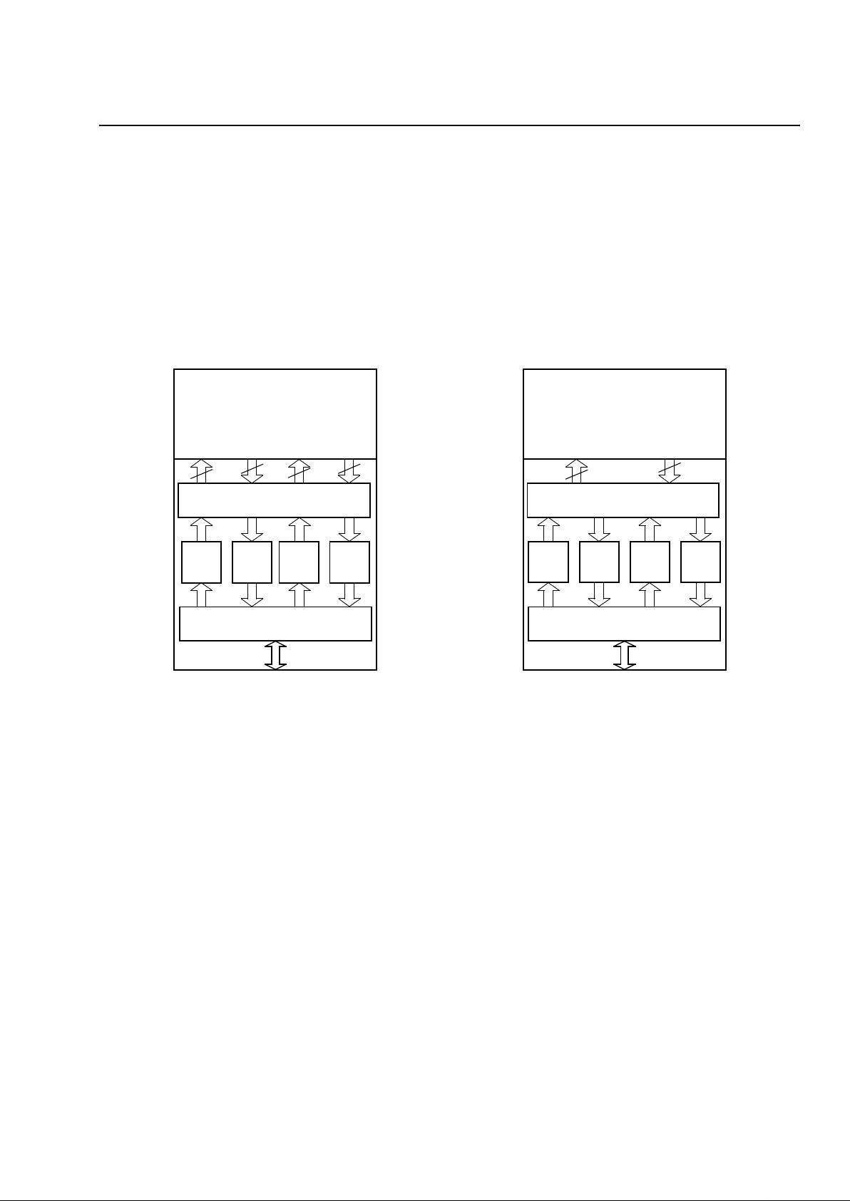
Diagrams for dual-port and quad-port operation are shown in Figure 1.
5-6368(F).e
Note: User I/O pin count includes three ExpressCLK pins.
Figure 1.
ORCA
OR3LP26B PCI FPSC Block Diagram
Embedded Core Options/FPGA Configuration
In addition to the Series 3 FPGA configuration modes (less Master parallel), the OR3LP26B can also be configured
via the PCI bus. Configuration as discussed here has two meanings. There is configuration of the FPGA logic, and
there is configuration of the options available in the embedded core. Both are accomplished through the FPGA
configuration process (some PCI configuration options may also be set via registers within the PCI bus core).
Readback of FPGA and PCI core options is also possible using the PCI bus or Series 3 FPGA readback modes.
The PCI bus core will be functional in the default PCI bus configuration space, as defined in the PCI bus 2.2 specification, prior to an initial configuration of the FPGA logic or the embedded core options.
113 USER I/O PADS
OR3T SERIES FPGA
18 ROWS x 28 COLUMNS
73
USER
I/O PADS
73
USER
I/O PADS
PCI
MASTER/TARGET
INTERFACE
PCI
BUS
DATA CONTROL
AND
MULTIPLEXING
32 32
32 32
64-bit x
16 DEEP
FIFO
TARGET
64-bit x
16 DEEP
FIFO
TARGET
64-bit x
32 DEEP
FIFO
MASTER
64-bit x
32 DEEP
FIFO
MASTER
113 USER I/O PADS
OR3T SERIES FPGA
18 ROWS x 28 COLUMNS
73
USER
I/O PADS
73
USER
I/O PADS
64-bit x
32 DEEP
FIFO
PCI
MASTER/TARGET
INTERFACE
PCI
BUS
DATA CONTROL
AND
MULTIPLEXING
64
64
MASTER
64-bit x
32 DEEP
FIFO
MASTER
64-bit x
16 DEEP
FIFO
TARGET
64-bit x
16 DEEP
FIFO
TARGET
Page 14

ORCA
OR3LP26B FPSC Data Sheet
Embedded Master/Target PCI Interface
March 2000
14 Lucent Technologies Inc.
Lucent Technologies Inc.
PCI Bus Core Detailed Description
The following sections describe the operation of the embedded core PCI bus interface.
PCI Bus Commands
The PCI core supports all commands required by the PCI specification. The following table describes each command. Subsequent sections will describe the protocols in which the commands are used.
Table 4. PCI Bus Command Descriptions
Command
Code
(Binary
)
Command
Master
Generates
Target
Accepts
Description
0000 Interrupt
Acknowl-
edge
— — Only implemented as Master by agents that interface to the sys-
tem CPU and as Target by agents that incorporate the system
interrupt controller.
0001 Special
Cycle
— — Target ignores, per PCI Specification section 3.6.2.
0010 I/O Read
√√
Fully implemented.
Target:
Bursting is prevented by disconnecting with data on the
first data phase. If signal
deltrn
is asserted low, I/O (and memory)
reads are handled as delayed transactions; no wait-states are
generated. If signal
deltrn
is deasserted high, the unit waits for the
data from the FPGA application, inserting wait-states (up to the
maximum allowed, after which a retry is issued).
Master:
Bursting is allowed, and no wait-states are generated.
0011 I/O Write
√√
Fully implemented.
Target:
Bursting is prevented by disconnecting with data on the
first data phase. If signal
deltrn
is asserted low, I/O writes are
handled as delayed transactions; no wait-states are generated.
Master:
Bursting is allowed, and no wait-states are generated.
0100 (reserved) — — Target ignores, per PCI Specification section 3.1.1.
0101 (reserved) — — Target ignores, per PCI Specification section 3.1.1.
0110 Memory
Read
√√
Fully implemented.
Target:
Bursting is allowed. If signal
deltrn
is asserted low, mem-
ory (and I/O) reads are handled as delayed transactions. If signal
deltrn
is deasserted high, the unit waits for the data from the
FPGA application, inserting wait-states (up to the maximum
allowed, after which a retry is issued). If signal
trburstpendn
is
asserted low and the Target Read FIFO is empty, wait-states are
inserted (up to the maximum allowed, after which a retry is
issued).
Master:
Bursting is allowed, and no wait-states are generated.
Page 15

Lucent Technologies Inc. 15
Data Sheet
ORCA
OR3LP26B FPSC
Marc h 2000 Embedded Master/Target PCI Inte rface
Lucent Technologies Inc.
PCI Bus Core Detailed Description
(continued)
Table 4. PCI Bus Command Descriptions
(continued)
Command
Code
(Binary
)
Command
Master
Generates
Target
Accepts
Description
0111 Memory
Write
√√
Fully implemented.
Target:
Writes are posted, bursting is allowed, and no wait-states
are generated.
Master:
Bursting is allowed, and no wait-states are generated.
1000 (reserved) — — Target ignores, per PCI Specification section 3.1.1.
1001 (reserved) — — Target ignores, per PCI Specification section 3.1.1.
1010 Configura-
tion Read
√√
Fully implemented.
Target:
Bursting is disallowed, and no wait-states are generated.
Target disconnects with data on first data word. The FPGA portion
of the device is not involved in Target configuration transactions.
Master:
Bursting is allowed, and no wait-states are generated.
1011 Configura-
tion Write
√√
Fully implemented.
Target:
Bursting is disallowed, and no wait-states are generated.
Target disconnects with data on first data word. The FPGA portion
of the device is not involved in Target configuration transactions.
Master:
Bursting is allowed, and no wait-states are generated.
1100 Memory
Read
Multiple
√√
Fully implemented. Both the Master and the Target treat this
instruction the same as a memory read (0110); the user’s FPGA
logic is responsible for ensuring that the Master operation meets
the special requirement that the read request ends on a cacheline
boundary.
1101 Dual
Access
Cycle
√√
Fully implemented. Per PCI Specification section 3.9, the PCI core
will automatically convert a 64-bit address to a 32-bit address if
the upper 32 bits are all zeros.
1110 Memory
Read Line
√√
Fully implemented. Both the Master and the Target treat this
instruction the same as a memory read (0110); the user’s FPGA
logic is responsible for ensuring that the Master operation meets
the special requirement that the read request continues to the next
cacheline boundary.
1111 Memory
Write and
Invalidate
√√
Fully implemented. Both the Master and the Target treat this
instruction the same as a memory write (0111); the user’s FPGA
logic is responsible for ensuring that the Master operation meets
the special requirement that writes of complete cachelines, with all
byte enables, are performed.
Page 16

1616 Lucent Technologies Inc.
ORCA
OR3LP26B FPSC Data Sheet
Embedded Master/Target PCI Interface March 2000
Lucent Technologies Inc.
PCI Bus Core Detailed Description
(continued)
PCI Protocol Fundamentals
Basic Transfer Control
The following paragraphs describe various aspects of
the PCI protocol and the way they are handled by the
PCI core.
Addressing.
The PCI Specification defines three types
of address spaces. The first, configuration address
space, is a physical address of space and is intended
as a means for powerup software to identify agents and
configure them before other address spaces have allocated. The second, I/O address space, is intended for
mapping control functions. Control function page sizes
in configuration space should be no more than
256 bytes. The third, memory address space, is
intended for bulk data transfer. It has features to facilitate this, such as special commands for cache implementation, large page sizes, and mechanisms for
prefetching. The PCI core handles all three address
space types as both a Master and a Target.
Byte Alignment.
On all write operations (configuration,
I/O, and memory space, and including the memory
write and invalidate instruction), for both the PCI core’s
Master and Target functions, byte enables are fully
implemented from/to the FPGA interface. Note, however, that even though the PCI core implements the
ability to control byte enables for the memory write and
invalidate instruction, the PCI Specification requires
that this instruction assert all byte enables, and this is
the FPGA application’s responsibility. On read operations, the utility of byte enables is more dubious since
the data must be enroute from the PCI bus from Target
to Master, at the time that the corresponding byte
enables are enroute on the PCI bus Master to Target
(unless wait-states are inserted). The PCI core, therefore, does not implement byte enable control for Master
or Target reads. Byte enables on master read operations are always asserted, and target ignores the byte
enables that are sent, in accordance with PCI Specification requirements.
Device Selectio n (devseln)
The target is responsible for responding to a master’s
request by asserting the PCI bus signal
devseln
.
devseln
may be asserted one, two, or three clocks
after the address phrase of a transaction, corresponding to fast, medium, or slow decode, respectively. The
PCI core’s target is capable of preforming a mediumspeed decode response. The decode response speed
has a significant impact on the overall latency and
bandwidth of nonburst PCI transactions, but its impact
decreases greatly for burst transactions, particularly for
burst lengths of the size of the PCI core’s FIFOs.
Address/Data Stepping
Stepping is an optional feature added to the PCI Specification to accommodate agents whose bus drive capability is insufficient to handle large groups of signals
changing state in one clock cycle. Continuous stepping
allows weak drivers multiple cycles for signal transition.
Discrete stepping partitions the bus into two or more
groups of bits that transition on successive clock
cycles. However, stepping exacts a heavy toll on performance, cutting maximum bandwidth by at least 50%
and increasing latency. The PCI core is designed for
maximum throughput with high-performance buffers, so
stepping is unnecessary and not implemented. The
wait cycle control, bit 7 of the command register, is
therefore hardwired to a zero.
Reset Operation
The PCI bus contains a signal,
rstn
, that performs a
PCI reset function. When the reset occurs, all state
machines in the ASIC are placed in their idle state, the
configuration space BARs are reset to their mask values, and the command registers are reset. The reset
does not reset the FPGA logic. The PCI reset signal is
fed from the ASIC to the FPGA logic to be used by the
designer.
Interrupt Acknowledge
The interrupt acknowledge command is a read by the
system CPU implicitly addressed to the system interrupt controller. Other agents, including the PCI core,
are not required to implement this instruction; the PCI
core’s Master does not generate it and its Target
ignores it.
Page 17

Lucent Technologies Inc. 17
Data Sheet
ORCA
OR3LP26B FPSC
Marc h 2000 Embedded Master/Target PCI Inte rface
Lucent Technologies Inc.
PCI Bus Core Detailed Description
(continued)
Arbitration Parking
The PCI Specification requires that all master agents
properly handle bus parking, which means that when
that agent receives an asserted
gntn
without the agent
having asserted
reqn
, the agent still must drive signal
par
and buses AD and c_ben. The PCI core meets this
requirement.
Parity
The PCI core implements all required and optional features, including the following:
■
Master generates parity on all addresses placed on
the bus.
■
Sending agent generates parity on all data placed on
the bus.
■
Target calculates parity on all addresses received
from the bus.
■
Receiving agent calculates parity on all data
received from the bus.
■
The detected parity error bit in the status register is
set whenever an agent calculates corrupted parity.
■
The signal
perrn
is generated whenever an agent
calculates corrupted parity and the parity error
response bit is set in the command register.
66 MHz Operation
The PCI core is fully compliant to PCI Specification
requirements at all clock rates up to 66 MHz. All
33 MHz requirements are also met.
Timing Budget
The PCI core’s timing budget is summarized in Table 5.
Note that the 66 MHz timing requirements only allow
5 ns for signal propagation (T
PROP
), as compared to
10 ns at 33 MHz. The effect of the reduction is to also
reduce the number of agents that the bus can support,
although the actual number is not specified in the PCI
Specification and is dependent on the design of the
hardware components. The four components of the
timing budget are T
VAL
(valid output delay), T
PROP
(propagation time), T
SU
(input setup time), and T
SKEW
(clock sk ew); o f these, only T
VAL
and T
SU
are controlled
by the PCI component, and T
PROP
and T
SKEW
are system parameters. Table 5 includes a third column (also
shown in the PCI Specification). This column indicates
the performance attainable if all 66 MHz requirements
are met except T
PROP
= 10 ns, which is the 33 MHz
value. In this case, the total budget increases from
15 ns (66 MHz) to 20 ns (50 MHz).
Table 5. Timing Budgets
64-Bit Addressing
The PCI core fully supports 64-bit addressing, whether
or not the PCI core is configured to utilize the 64-bit
data extension. When the PCI core is a 64-bit target
being addressed by 64-bit master, the PCI core will
decode the address one cycle faster so that dualaddress operation will have no performance impact;
see PCI Specification section 3.9 for details.
Section 3.9 of the PCI Specification also states that a
Master that supports 64-bit addressin g must nevertheless generate requests utilizing a single address
instead of a dual address when the upper 32 bits are all
zeros. This shortens the request time by one cycle
when comm unicati ng wit h 32-bit Targets. It is the FPGA
application’s responsibility to ensure that this requirement is met.
FIFO Memories and Control
The OR3LP26B embedded core contains four FIFO
memories and supporting control logic. Two FIFOs are
for the master interface data and two for the target
interface data. These FIFOs are always configured to
operate in 64-bit mode and also carry byte enable bits
on a per-byte basis (e.g., the 64-bit FIFO actually carries 64 bits of data and 8 byte enable bits for a total of
72 bits). During 32-bit transactions, the FPSC will pack
the data to fully utilize the memories. All FIFOs have
four flags: Full, Almost Full (Full-4), Empty, and Almost
Empty (Empty+4). (See Table 6.) The FPGA application is provided with the Full/Empty signal and Almost
Full/Empty signal associated with the FPGA side of the
FIFO. In addition, the FPGA application is provided
with the PCI side's Full/Empty signal (but not the
Almost Full/Empty signal), to enable checking for operation completion. Clocking for the FPGA side of all
FIFOs is flexible, with options for different clocks f or the
Master and Target FIFOs, sourced by the FPGA logic,
or by the PCI bus clock.
Timing Element 33 MHz 50 MHz 66 MHz Unit
Cycle Time 30.0 20.0 1 5.0 ns
Valid Output
Delay
11.0 7.5 6.0 ns
Propagation
Time
10.0 6.5 5.0 ns
Input Setup Time 7.0 4.5 3.0 ns
Clock Skew 2.0 1.5 1.0 ns
Page 18

ORCA
OR3LP26B FPSC Data Sheet
Embedded Master/Target PCI Interface
March 2000
18 Lucent Technologies Inc.
Lucent Technologies Inc.
PCI Bus Core Detailed Description
(continued)
Table 6. FIFO Flags Provided to FPGA Application
PCI Bus Pin Information
This section describes signals on the PCI bus interface and at the embedded core/FPGA interface. Some signal
definitions change name and location based on the mode of operation. Modes of operation are described following
the signal descriptions. PCI bus signal package pin locations can be found in Table 70.
Table 7. PCI Bus Pin Descriptions
Write Operation Read Operation
FPGA Side PCI Side FPGA Side PCI Side
Master Operation
mw_fulln mw_emptyn mr_emptyn mr_fulln
mw_afulln mr_aemptyn
Target Operation
tw_emptyn tw_fulln tr_fulln tr_emptyn
tw_aemptyn tr_afulln
S
y
mbol
I/O
Description
System Pins
clk
I
Clock.
Provides timing for all transactions on the PCI bus and is an input to the
OR3LP26B device. All PCI signals, except
rstn
and
intan
, are sampled on the ris-
ing edge of
clk
, and all other PCI bus timing parameters are defined with respect to
this edge. The signal
clk
operates up to 66 MHz, and the minimum frequency is dc.
rstn I
Reset.
An active-low signal used to reset the entire PCI bus.
rstn
is asynchronous
to
clk
. During
rstn
, all PCI output signals are 3-stated.
Address and Data Pins
ad[31:0] I/O
Address and Data.
Multiplexed on the same PCI pins. A PCI bus transaction con-
sists of an address phase followed by one or more data phases.
During data phases,
ad[7:0]
contain the least significant byte and
ad[31:24]
con-
tain the most significant byte. During memory commands, the
ad[31:2]
lines spec-
ify the address and
ad[1:0]
specify the type of bursting sequence to use. The table
below outlines the bursting sequence based on the values of
ad[1:0]
.
ad[1:0]
Bursting sequence.
00 Linear incrementing.
01 Disconnect after first transfer.
10 Disconnect after first transfer.
11 Disconnect after first transfer.
c_ben[3:0] I/O
Bus Command and Byte Enables.
Active-low signals multiplexed on the same
PCI pins. During the address phase of a transaction,
c_ben[3:0]
define the bus
command. During the data phase,
c_ben[3:0]
are used as byte enables. The byte
enables are valid for the entire data phase and determine which byte lanes carry
meaningful data.
par I/O
Parity.
Specifies even parity across
ad[31:0]
and
c_ben[3:0]. par
is stable and
valid one clock after the address phase. For data phases,
par
is stable and valid
one clock after
irdyn
is asserted on a write transaction or
trdyn
is asserted on a
read tran sa cti o n. Once
par
is valid, it remains valid until one clock after the comple-
tion of the current data phase. The Master drives
par
for address and write data
phases; the Target drives
par
for read data phases.
Page 19

Lucent Technologies Inc. 19
Data Sheet
ORCA
OR3LP26B FPSC
Marc h 2000 Embedded Master/Target PCI Inte rface
Lucent Technologies Inc.
PCI Bus Core Detailed Description
(continued)
Table 7. PCI Bus Pin Descriptions
(continued)
S
y
mbol
I/O
Description
Interface Control Pins
framen I/O
Cycle Frame.
An active-low signal driven by the current Master to indicate the
beginning and duration of an access. The signal framen is asserted to indicate a
bus transaction is beginning. While
framen
is asserted, data transfers continue.
When
framen
is deasserted, the transaction is in the final phase or has completed.
irdyn I/O
Initiator Ready.
An active-low signal indicating the bus Master’s ability to complete
the current data phase of the transaction. The signal
irdyn
is used in conjunction
with
trd
y
n
. A data phase is completed on any clock cycle during which both
irdyn
and
trd
y
n
are asserted. Duri ng a write ,
irdyn
indicates that valid data is present on
ad[31:0]
. During a read, it indicates the Master is prepared to accept data. Wait
cycles are inserted until both
irdyn
and
trd
y
n
are asserted together.
trd
y
n
I/O
Target Ready.
An active-low signal asserted to indicate the readiness of the Tar-
get’s agent to complete the current data phase of the transaction. The signal
trd
y
n
is used in conjunction with
irdyn
. A data phase is completed on any clock where
both
trd
y
n
and
irdyn
are sampled active. During reads,
trdyn
indicates that valid
data is present on
ad[31:0]
lines. During write cycles,
trd
y
n
indicates that the Tar-
get is prepared to accept data.
stopn
I/O
STOPn.
Indicates that the current Target is requesting the Master to stop the cur-
rent transaction.
idsel I
Initialization Device Select.
Used as a chip select during PCI configuration read
and write transactions. Generally, the user ties
idsel
to one of the upper 24 address
lines,
ad[31:8]
.
devseln I/O
Device Select.
An active-low input indicating that a device on the bus has been
selected. As an output, it indicates that the driving device has decoded its address
as the Target of the current access.
Arbitration Pins (for Bus Master Only)
reqn O
Request.
An active-low signal that indicates to the arbiter that the asserting agent
desires use of the bus. In the OR3LP26B, this signal is asserted when the
OR3LP26B Master controller needs access to the PCI bus.
gntn I
Grant.
An active-low signal that indicates to the OR3LP26B that access to the PCI
bus has been granted.
Error Reporting Pins
perrn I/O
Parity Error.
An active-low signal for the reporting of data parity errors during all
PCI transact i ons except a sp e ci al cy cl e. The
perrn
pin is a sustained 3-state signal
and must be driven active by the agent receiving data two clocks following the data
when a data parity error is detected. The minimum duration of
perrn
is one clock for
each data phase that a data parity error is detected. If sequential data phases each
have a data parity error, the
perrn
signal will be asserted for more than a single
clock.
perrn
is driven high for one clock before being 3-stated. The signal
perrn
is
not asserted until it has claimed the access by asserting
devseln
and completed a
data phase.
Page 20

ORCA
OR3LP26B FPSC Data Sheet
Embedded Master/Target PCI Interface
March 2000
20 Lucent Technologies Inc.
Lucent Technologies Inc.
PCI Bus Core Detailed Description
(continued)
Table 7. PCI Bus Pin Descriptions
(continued)
S
y
mbol
I/O
Description
serrn
O
System Error.
An active-low open drain signal pulsed by agents to report errors
other than parity.
serrn
is sampled every
clk
edge, so any agent asserting
serrn
must ensure it is valid for at least one clock period. The OR3LP26B asserts
serrn
if
a Master abort sequence is asserted when the Master controller is accessing the
PCI bus.
Interrupt Pins
intan O
PCI Interrupt.
The OR3LP26B asserts this active-low open drain signal when it
requests an interrupt from the PCI compliant interrupt controller.
64-Bit Bus Extension Pins
ad[63:32] I/O
64-Bit Address and Data.
These signals provide the upper 32 bits of address and
data when in PCI 64-bit operation. During an address phase (when using the DAC
command and when
req64n
is asserted), these address bits are transferred. Dur-
ing a data phase, the data is valid when
req64n
and
ack64n
are both asserted.
Otherwise, these bits are 3-stated.
c_ben[7:4] I/O
Byte Enables.
These are the upper four, active-low, bus command and byte
enables when in PCI 64-bit operation. During an address phase (when using the
DAC command and when
req64n
is asserted), the bus command is transferred.
During a data phase, these bits are the active-low byte enables for data bits 64:32.
Otherwise, these bits are 3-stated.
req64n I/O
Request 64-Bit Transfer.
This active-low signal is asserted by the current bus
Master to indicate that it desires to transfer data using 64 bits. The signal
req64n
has the same meaning as
framen
for 32-bit transfers.
ack64n I/O
Acknowledge 64-Bit Transfer.
The Target drives this signal low to indicate that it
has decoded its own address as the Target of the current access and that it can do
64-bit transfers. The signal
ack64n
has the same timing as
devseln
in 32-bit trans-
fers.
par64 I/O
Upper Double-Word Parity.
The even parity bit that covers
ad[63:32]
and
c_ben[7:4]
. PAR64 is valid one clock after the initial address phase when
req64n
is
asserted and the DAC command is indicated on
c_ben[7:4]
. It is also valid the
clock cycle after the second address phase of a DAC command when
req64n
is
asserted.
Hot Swap Function Pins
enumn O Active-low open drain signal that notifies the system host that the card has been
freshly inserted or is about to be extracted. The system host can then either install
(for insertion) or quiesce (for extraction) the card’s driver to adjust for the change in
system configuration.
ledn O Active-low open-drain signal that drives a blue LED, indicating that removal of the
card is permitted. This signal is asserted low whenever the LED ON/OFF (LOO) bit
in the hot swap control and status register (HSSCR) is asserted high.
ejectsw I Active-high signal that indicates that the card’s ejector handle is unseated. This sig-
nals that the operator has freshly inserted the card, or will extract the card when the
blue LED illuminates. If not used, tie high or low.
vio I
PCI Bus Signaling Environment Voltage.
This input indicates to the PCI core the
signaling environment being employed on the PCI bus. The input is tied to the
appropriate voltage supply (either 5.0 V or 3.3 V).
Page 21

Lucent Technologies Inc. 21
Data Sheet
ORCA
OR3LP26B FPSC
Marc h 2000 Embedded Master/Target PCI Inte rface
Lucent Technologies Inc.
PCI Bus Core Detailed Description Dual Port
Pages 21—69 will refer to the dual-port mode of the OR3LP26B device. For quad-port mode, please refer to pages
70—122.
Embedded Core/FPGA Interface Signal Descriptions
In Table 8, an input refers to a signal flowing into the FPGA logic (out of the embedded core) and an output refers
to a signal flowing out of the FPGA logic (into the embedded core).
Table 8
. Embedded Core/FPGA Interface Si
g
nals
Symbol I/O Description
Data FIFO Signals
datafmfpga[63:0]
datafmfpgax[7:0]
O
Main data bus into the master write FIFO and target read FIFO. Refer to Table 10 on
page 30 for bus usage and bit descriptions.
These signals must be synchronous to
fclk
.
datatofpga[63:0]
datatofpgax[7:0]
I
Main data bus out of the master read FIFO and target write FIFO. Refer to Table 10
on page 30 for bus usage and bit descriptions.
These signals are synchronous to
fclk
.
Master General Signals
fpga_mbusyn
O
FPGA Master Is Busy .
This signal is used in modes currently not implemented in the
core. Tie off this signal to a 1.
fpga_msyserror
I
FPGA Master Cycle Aborted by PCI Target.
The PCI Master controller in the PCI
core asserts this active-high as an indication that the current cycle to the PCI bus has
been aborted. This signal is synchronous to
fclk
.
mcfgshiftenn
pci_mcfg_stat
OImcfgshiftenn is an active-low si gnal that determines the data that is output by the PCI
core onto signal
pci_mcfg_stat
:
mcfgshiftenn
= 1:
pci_mcfg_stat
= wired-OR of all bits below, after being
masked by FPGA configuration RAM bits;
mcfgshiftenn
= 0:
pci_mcfg_stat
= each bit below, one at a time on succes-
sive
pciclk
rising edges (unmasked), reset when
mcfgshiftenn
= 1;
Status bits: Data parity error detected, Target abort received, and
Master abort received.
Both signals are synchronous to
fclk
.
Master FIFO Address and Command Register Control Signals
S
y
mbol I/O Description
maenn O
Master Command/Address/Burst Length Enable.
This is an active-low signal and
is used to enable registering commands , burst length, and start address into the Master address register of the PCI core. On each rising edge of the clock that this signal
is sampled low, command, burst length, and address will be registered.
This signal must be synchronous to
fclk
.
ma_fulln
I
Master Address Register Full Flag.
This active-low signal indicates that the Master
address register is full and no more addresses can be registered.
This signal is synchronous to
fclk
.
mstatecntr[2:0]
I
Internal State Counter.
Used for Master reads and writes. Details of the Master state
machine operation can be found in tables at the end of each operation section.
This signal is synchronous to
fclk
.
mfifoclrn
O
Master FIFO Clear.
This active-low signal i s asserted by the FPGA Master to clear all
Master FIFOs.
This signal must be synchronous to
fclk
.
Page 22

ORCA
OR3LP26B FPSC Data Sheet
Embedded Master/Target PCI Interface
March 2000
22 Lucent Technologies Inc.
Lucent Technologies Inc.
PCI Bus Core Detailed Description Dual Port
(continued)
Table 8. Embedded Core/FPGA Interface Si
g
nals
(continued)
S
y
mbol
I/O
Description
m_ready
I
Master Logic Ready.
This active-high signal indicates that the Master logic
interfacing to the FPGA logic is ready. This signal will be inactive during PCI bus
reset or Master FIFO clears.
This signal is synchronous to
fclk
.
mcmd[3:0]
O
Master Command Code.
Command code for the current Master read/write
operation. Refer to Table 10 on page 30.
This signal must be synchronous to
fclk
.
Master Write Data FIFO Signals
mwdataenn
O
Master Write FIFO Data Enable.
This active-low signal enables the registering
of bus
datafmfpga
during Master write operations into the PCI core Master
write data FIFOs on the rising edge of the Master FIFO clock signal. The signal
mwdataenn
should not be asserted when the Master write data FIFOs are full,
or data may be lost.
This signal must be synchronous to
fclk
.
mwpcihold
O
Master Write PCI Bus Hold.
During burst transfers on the PCI bus, this signal
delays the start of the transfer on the PCI bus, allowing the FPGA application to
fill the FIFO. The transaction will begin when
mwpcihold
is deasserted or the
FIFO becomes full. When asserted,
mwpcihold
must be held low for a mini-
mum of two
pciclk
periods.
This signal must be synchronous to
pcilk
.
mw_fulln
I
Master Write Data FIFO Full Flag.
This active-low signal indicates that the
Master write data FIFOs are full.
This signal is synchronous to
fclk
.
mw_afulln
I
Master Write Data FIFO Almost Full Flag.
This active-low signal indicates that
only four more empty locations remain in the Master write data FIFOs.
This signal is synchronous to
fclk
.
mw_emptyn
I
Master Write Data FIFO Empty Flag.
This active-low signal indicates that the
Master write data FIFO is empty. Refer to Master write description on signal
usage.
This signal is synchronous to
pciclk
.
mwlastcycn O
Master Write Last Data Cycle.
This active-low signal has two functions:
a. It is asserted low to indicate that the accompanying 32/64 bits of Master read
or write address information is the final portion being sent. It can also be
asserted prior to any address portion being sent, indicating that the previous
address is to be used.
b. It is asserted low to indicate that the accompanying master write data is the
final data for this operation. When more than one cycle is required to transfer
a complete data word, this signal is only valid on the last cycle.
This signal must be synchronous to
fclk
.
Master Read Data FIFO Signals
mrdataenn O
Master Read FIFO Data Output Enable.
This active-low signal enables the
data from the PCI core Master read data FIFOs onto bus
datatofpga
during
Master read operations on the rising edge of the Master FIFO clock signal. Valid
data will be read from the FIFO whenever it is not empty.
This signal must be synchronous to
fclk
.
mr_emptyn I
Master Read Data FIFO Empty.
This active-low signal indicates that the Master read data FIFOs of the PCI core are empty.
This signal is synchronous to
fclk
.
Page 23

Lucent Technologies Inc. 23
Data Sheet
ORCA
OR3LP26B FPSC
Marc h 2000 Embedded Master/Target PCI Inte rface
Lucent Technologies Inc.
PCI Bus Core Detailed Description Dual Port
(continued)
Table 8. Embedded Core/FPGA Interface Si
g
nals
(continued)
S
y
mbol
I/O
Description
mr_aemptyn I
Master Read Data FIFO Almost Empty.
This active-low signal indicates that
only four more data locations are available to be read from the Master read data
FIFOs of the PCI core.
This signal is synchronous to
fclk
.
mr_fulln I
Master Read Data FIFO Full Flag.
This active-low signal indicates that the
Master read data FIFO is full. Refer to Master read description on signal usage.
This signal is synchronous to
pciclk
.
fpga_mstopburstn O
Stop Burst Reads.
This active-low signal is used by the FPGA Master to terminate burst reads before completion. When asserted, it must stay asserted for a
minimum of two
pciclk
periods. When asserted,
fpga_mstopburstn
must stay
asserted until
ma_fulln
goes inactive (high).
This signal must be synchronous to
pciclk
.
mrlastcycn I
Master Read Last Data Cycle.
This active-low signal is asserted to indicate
that the accompanying Master read data is the final data for this operation.
When more than one cycle is required to transfer a complete data word, this
signal is only valid on the last cycle (1
fclk
period).
This signal is synchronous to
fclk
.
Target General Signals
disctimerexpn I
Discard Timer Expired.
This active-low signal, when asserted, indicates that
the discard timer has expired and the core will now treat the retried delayed
transaction as a new transaction. The discard timer is a 15-bit counter which
starts its count when a delayed transaction is started.
This signal is synchronous to
fclk
.
fpga_tabort O
Target Abort.
This active-high signal is asserted by the FPGA Target application to abort all future PCI cycles. Once asserted, this signal needs to remain
asserted for a minimum of two
pciclk
cycles.
This signal must be synchronous to
pciclk
.
fpga_tretryn O
Assert Retry.
This active-low signal is asserted by an FPGA Target to the PCI
core to send a retry to the PCI bus. Once asserted, this signal needs to remain
asserted for a minimum of two
pciclk
cycles.
This signal must be synchronous to
pciclk
.
deltrn O
Target Delayed Transaction.
Used for Target I/O write (page 50) and Target
read operations (page 59). Target memory writes are always posted. Once
asserted, this signal needs to remain asserted for a minimum of two
pciclk
cycles.
This signal must be synchronous to
pciclk
.
tcfgshiftenn
pci_tcfg_stat
O
I
tcfgshiftenn
is an active-low signal that determines the data that is output by
the PCI core onto signal
pci_tcfg_stat
:
tcfgshiftenn
= 1:
pci_tcfg_stat
= wired-OR of all bits below, after being
masked by FPGA configuration RAM bits;
tcfgshiftenn
= 0:
pci_tcfg_stat
= each bit below, one at a time on suc-
cessive pciclk rising edges (unmasked), reset when
tcfgshiftenn
= 1;
Status bits: Target abort signaled, system error signaled,
and parity error detected.
Both signals are synchronous to
fclk
.
Page 24

ORCA
OR3LP26B FPSC Data Sheet
Embedded Master/Target PCI Interface
March 2000
24 Lucent Technologies Inc.
Lucent Technologies Inc.
PCI Bus Core Detailed Description Dual Port
(continued)
Table 8. Embedded Core/FPGA Interface Si
g
nals
(continued)
S
y
mbol
I/O
Description
Target FIFO Address and Command Register Control Signals
tfifoclrn O
Target FIFO Clear.
This active-low signal is asserted by the FPGA Target to
clear all Target FIFOs.
This signal must be synchronous to
fclk
.
treqn I
Target Request from PCI.
This active-low signal is synchronous to the Target
FIFO clock signal. The PCI core asserts
treqn
as an indication to the Target
that a transfer request (either read or write) is pending to the target. As long as
there are valid target addresses present in the address FIFO, the treqn signal
will continue to be active.
This signal is synchronous to
fclk
.
t_ready I
T a rget Logic Ready.
This active-high signal indicates that the T arget logic interfacing to the FPGA logic is ready. This signal will be inactive during PCI bus
reset or Target FIFO clears.
This signal is synchronous to
fclk
.
taenn O
Target Address and Command Register Output Enable.
This active-low signal enables PCI addresses to be read from the Target address register of the
PCI core, and PCI commands to be read from the Target command register.
The PCI core will only execute enough address cycles to transfer the address
within the matched page (higher-order bits are not stripped).
This signal must be synchronous to
fclk
.
tcmd[3:0] I
Target Command Code.
This bus provides the command code for a new Tar-
get operation, and is valid when the FPGA senses
treqn
active-low.
Because it is synchron ous to
pciclk
, it must be qualified with
treqn
.
bar[2:0] I
Base Address Register Number.
This bus indicates which of the six BARs
matched the address for the current Target operation, and is valid when the
FPGA senses
treqn
active-low. The three 64-bit BARs are designated as numbers 0, 2, and 4.
Because it is synchron ous to
pciclk
, it must be qualified with
treqn
.
tstatecntr[2:0] I
Internal State Counter.
Used for target reads and writes. Details of the target
state machine operation can be found in tables at the end of each operation
section.
This signal is synchronous to
fclk
.
Target Write Data FIFO Signals
twdataenn O
Target Write FIFO Data Enable.
This active-low signal enables data from the
PCI core Target write da t a F I FOs on t o bus
datatofpga
during Target write operations on the rising edge of the Target FIFO clock signal. Valid data will be read
from the FIFO whenever it is not empty.
This signal must be synchronous to
fclk
.
tw_emptyn I
Target Write FIFO Empty.
This signal active indicates that the Target write
FIFO is empty.
This signal is synchronous to
fclk
.
tw_aemptyn I
Target Write FIFO Almost Empty.
This active-low signal indicates that only
four more empty locations are available in the Target write FIFOs.
This signal is synchronous to
fclk
.
tw_fulln I
Target Write Data FIFO Full Flag
. This active-low signal indicates that the target write data FIFO is full. Refer to target write description on signal usage.
This signal is synchronous to
pciclk
.
Page 25

Lucent Technologies Inc. 25
Data Sheet
ORCA
OR3LP26B FPSC
Marc h 2000 Embedded Master/Target PCI Inte rface
Lucent Technologies Inc.
PCI Bus Core Detailed Description Dual Port
(continued)
Table 8. Embedded Core/FPGA Interface Signals
(continued)
S
y
mbol
I/O
Description
twlastcycn I
Target Write Last Data Cycle.
This active-low signal has two functions:
a. It is asserted low to indicate that the accompanying 32/64 bits of Target read or
write address information is the final portion being sent. It can also be asserted
prior to any address portion being sent, indicating that the previous address is
to be used.
b. It is asserted low to indicate that the accompanying T arget write data is the final
data for this operation. When more than one cycle is required to transfer a complete data word, this signal is only valid on the last cycle.
This signal is synchronous to
fclk
.
Target Read Data FIFO Signals
twburstpendn O
Target Write Burst Data Availability Pending Flag.
This active-low signal
directs the PCI core not to immediately disconnect when the Target write FIFO
becomes full, but rather to insert PCI bus wait-states (up to the maximum allowed,
and then disconnect). Once asserted, this signal needs to remain asserted for a
minimum of two
pciclk
periods.
This signal must be synchronous to
pciclk
.
trdataenn O
Target Read FIFO Data Enable.
This active-low signal enables the registering of
bus
datafmfpga
during Target read operations into the PCI core Target read data
FIFOs on the rising edge of the Target FIFO clock signal. The signal
trdataenn
should not be asserted when the Target read data FIFOs are full, or data may be
lost.
This signal must be synchronous to
fclk
.
tr_fulln I
Target Read FIFO Full.
This signal is active-low and synchronous to the rising
edge of the Target FIFO clock signal. The PCI core asserts this signal to indicate
that the Target read FIFOs are full and that no more data can be clocked in.
This signal is synchronous to
fclk
.
tr_afulln I
Target Read FIFO Almost Full.
This active-low signal indicates that the Target
read FIFO has only four more empty locations available in the FIFOs.
This signal is synchronous to
fclk
.
tr_emptyn I
Target Read Data FIFO Empty Flag.
This active-low signal indicates that the target read data FIFO is empty. Refer to target read description on signal usage.
This signal is synchronous to
pciclk
.
trpcihold O
Target Read PCI Bus Hold
. During burst transfers on the PCI bus, this signal
delays the start of the transfer on the PCI bus, allowing the FPGA application to fill
the FIFO. The transaction will begin when
trpcihold
is deasserted or the FIFO
becomes full. Once asserted, this signal needs to remain asserted for a minimum
of two
pciclk
periods.
This signal must be synchronous to
pciclk
.
trlastcycn I
Target Read Last Data Cycle.
This active-low signal is asserted to indicate that
the accompanying Target read data is the final data for this operation. When more
than one cycle is required to transfer a complete data word, this signal is only
valid on the last cycle. During a read burst,
trlastcycn
may remain inactive for
longer than it is required to complete the data transfer. If this occurs, the FPGA
Target should continue to write data into the Target read FIFOs unless the incremented address crosses the address decode space of the FPGA Target. The
address should be incremented by a double word as long as
trlastcycn
is inactive.
This signal is synchronous to
fclk
.
Page 26

ORCA
OR3LP26B FPSC Data Sheet
Embedded Master/Target PCI Interface
March 2000
26 Lucent Technologies Inc.
Lucent Technologies Inc.
PCI Bus Core Detailed Description Dual Port
(continued)
Table 8. Embedded Core/FPGA Interface Signals
(continued)
S
y
mbol
I/O
Description
trburstpendn O
Target Read Burst Data Availability Pending Flag.
This active-low signal
directs the PCI core not to immediately disconnect when the Target read FIFO
becomes empty, but rather to insert PCI bus wait-states (up to the maximum
allowed, and then disconnect). Once asserted, this signal needs to remain
asserted for a minimum of two
pciclk
periods.
This signal must be synchronous to
pciclk
.
Miscellaneous Signals
pci_intan O
PCI Interrupt Request
. This active-low signal is used to generate a PCI bus
interrupt and is forwarded by the PCI core as
intan
onto the PCI bus. Once
asserted, this signal needs to remain asserted for a minimum of two
pciclk
cycles.
This signal must be synchronous to
pciclk
.
fclk1
fclk2
O
O
FPGA Clock 1 and 2
. Clocks for use by the PCI core for Master and Target
FIFOs. When the PCI clock domain extends into the FPGA, the FPGA may
reroute the PCI clock back into
fclk1
or
fclk2
. External or user-defined clocks may
also be used. The signals
fclk1
and
fclk2
must be the same clock in dual-port
mode.
pciclk I
PCI Clock
. The signal
pciclk
is synchronous to
clk
and may be used by the
FPGA logic.
pci_rstn I
PCI Reset for Use by the FPGA Logic
. This active-low signal indicates that a
PCI bus reset was received from the PCI bus (
rstn
).
fpga_syserror O
System Error
. This active-high signal is used by the FPGA to generate a system
error on the PCI bus. This is passed to the PCI bus as
serrn
.
This signal must be synchronous to
pciclk
.
pci_64bit I
PCI Bus in 64-Bit Mode
. This active-high signal indicates that the PCI core
detected that it is connected as a 64-bit agent to the PCI bus. This is the result of
detecting PCI signal
req64n
as active (low) on the inactive-going (rising) edge of
PCI signal
rstn
. Note that this does not imply that any particular transaction is
64-bit, since each transaction is individually negotiated using PCI signals
req64n
and
ack64n
.
This signal is synchronous to
pciclk
.
fifo_sel O
FIFO Select.
An active-high signal that is valid in the dual-port modes to select
either Master read data (
fifo_sel
= 0) or Target write data (
fifo_sel
= 1).
This signal must be synchronous to
fclk
.
Page 27

Lucent Technologies Inc. 27
Data Sheet
ORCA
OR3LP26B FPSC
Marc h 2000 Embedded Master/Target PCI Inte rface
Lucent Technologies Inc.
PCI Bus Core Detailed Description Dual Port
(continued)
Embedded Core/FPGA Interface Signal Locations
Table 9 lists the physical locations of all signals on the PCI core/FPGA interface. Separate names are provided for
dual-port and quad-port bus signals, since their functionality is port mode dependent.
Table 9. OR3LP26B FPGA/PCI Core Interface Signal Locations
PCI Core/FPGA Interface Site FPGA Input Signal Name FPGA Output Signal Name
ASB1A pci_rstn pci_intan
ASB1B pci_64bit (unused)
ASB1C (unused) fpga_syserror
ASB1D (unused) fpga_mbusyn
ASB2A datatofpga31 datafmfpga31
ASB2B datatofpga30 datafmfpga30
ASB2C datatofpga29 datafmfpga29
ASB2D datatofpga28 datafmfpga28
ASB3A datatofpga27 datafmfpga27
ASB3B datatofpga26 datafmfpga26
ASB3C datatofpga25 datafmfpga25
ASB3D datatofpga24 datafmfpga24
ASB4A datatofpga23 datafmfpga23
ASB4B datatofpga22 datafmfpga22
ASB4C datatofpga21 datafmfpga21
ASB4D datatofpga20 datafmfpga20
ASB5A datatofpga19 datafmfpga19
ASB5B datatofpga18 datafmfpga18
ASB5C datatofpga17 datafmfpga17
ASB5D datatofpga16 datafmfpga16
ASB6A datatofpgax3 datafmfpgax3
ASB6B datatofpgax2 datafmfpgax2
ASB6C datatofpgax1 datafmfpgax1
ASB6D datatofpgax0 datafmfpgax0
ASB7A datatofpga15 datafmfpga15
ASB7B datatofpga14 datafmfpga14
ASB7C datatofpga13 datafmfpga13
ASB7D datatofpga12 datafmfpga12
ASB8A datatofpga11 datafmfpga11
ASB8B datatofpga10 datafmfpga10
ASB8C datatofpga9 datafmfpga9
ASB8D datatofpga8 datafmfpga8
ASB9A datatofpga7 datafmfpga7
ASB9B datatofpga6 datafmfpga6
ASB9C datatofpga5 datafmfpga5
ASB9D datatofpga4 datafmfpga4
CKTOASB9 (unused) fclk1
Page 28

ORCA
OR3LP26B FPSC Data Sheet
Embedded Master/Target PCI Interface
March 2000
28 Lucent Technologies Inc.
Lucent Technologies Inc.
PCI Bus Core Detailed Description Dual Port
(continued)
Table 9. OR3LP26B FPGA/PCI Core Interface Signal Locations
(continued)
PCI Core/FPGA Interface Site FPGA Input Signal Name FPGA Output Signal Name
ASB10A datatofpga3 datafmfpga3
ASB10B datatofpga2 datafmfpga2
ASB10C datatofpga1 datafmfpga1
ASB10D datatofpga0 datafmfpga0
ASB11A tstatecntr0 (unused)
ASB11B tstatecntr1 (unused)
ASB11C tstatecntr2 (unused)
ASB11D pci_tcfg_stat tcfgshiftenn
ASB12A tcmd0 (unused)
ASB12B tcmd1 (unused)
ASB12C tcmd2 (unused)
ASB12D tcmd3 twburstpendn
ASB13A bar0 trburstpendn
ASB13B bar1 fpga_tabort
ASB13C bar2 fpga_tretryn
ASB13D disctimerexpn deltrn
ASB14A treqn taenn
ASB14B twlastcycn twdataenn
ASB14C tw_emptyn fifo_sel
ASB14D tw_aemptyn (unused)
CKFMASB14 pciclk (unused)
ASB15A t_ready tfifoclrN
ASB15B trlastcycn trdataenn
ASB15C tr_fulln (unused)
ASB15D tr_afulln (unused)
ASB16A tw_fulln trpcihold
ASB16B tr_emptyn mwpcihold
ASB16C mw_emptyn fpga_mstopburstn
ASB16D mr_fulln (unused)
ASB17A ma_fulln maenn
ASB17B mw_fulln mwdataenn
ASB17C mw_afulln mwlastcycn
ASB17D m_ready mrdataenn
ASB18A mrlastcycn mcmd0
ASB18B mr_emptyn mcmd1
ASB18C mr_aemptyn mcmd2
ASB18D fpga_msyserror mcmd3
ASB19A datatofpga32 datafmfpga32
ASB19B datatofpga33 datafmfpga33
ASB19C datatofpga34 datafmfpga34
ASB19D datatofpga35 datafmfpga35
CKTOASB19 (unused) fclk2
ASB20A datatofpga36 datafmfpga36
Page 29

Lucent Technologies Inc. 29
Data Sheet
ORCA
OR3LP26B FPSC
Marc h 2000 Embedded Master/Target PCI Inte rface
Lucent Technologies Inc.
PCI Bus Core Detailed Description Dual Port
(continued)
Table 9. OR3LP26B FPGA/PCI Core Interface Signal Locations
(continued)
PCI Core/FPGA Interface Site FPGA Input Signal Name FPGA Output Signal Name
ASB20B datatofpga37 datafmfpga37
ASB20C datatofpga38 datafmfpga38
ASB20D datatofpga39 datafmfpga39
ASB21A datatofpga40 datafmfpga40
ASB21B datatofpga41 datafmfpga41
ASB21C datatofpga42 datafmfpga42
ASB21D datatofpga43 datafmfpga43
ASB22A datatofpga44 datafmfpga44
ASB22B datatofpga45 datafmfpga45
ASB22C datatofpga46 datafmfpga46
ASB22D datatofpga47 datafmfpga47
ASB23A datatofpgax4 datafmfpgax4
ASB23B datatofpgax5 datafmfpgax5
ASB23C datatofpgax6 datafmfpgax6
ASB23D datatofpgax7 datafmfpgax7
ASB24A datatofpga48 datafmfpga48
ASB24B datatofpga49 datafmfpga49
ASB24C datatofpga50 datafmfpga50
ASB24D datatofpga51 datafmfpga51
ASB25A datatofpga52 datafmfpga52
ASB25B datatofpga53 datafmfpga53
ASB25C datatofpga54 datafmfpga54
ASB25D datatofpga55 datafmfpga55
ASB26A datatofpga56 datafmfpga56
ASB26B datatofpga57 datafmfpga57
ASB26C datatofpga58 datafmfpga58
ASB26D datatofpga59 datafmfpga59
ASB27A datatofpga60 datafmfpga60
ASB27B datatofpga61 datafmfpga61
ASB27C datatofpga62 datafmfpga62
ASB27D datatofpga63 datafmfpga63
ASB28A mstatecntr0 mfifoclrn
ASB28B mstatecntr1 (unused)
ASB28C mstatecntr2 (unused)
ASB28D pci_mcfg_stat mcfgshiftenn
Page 30

ORCA
OR3LP26B FPSC Data Sheet
Embedded Master/Target PCI Interface
March 2000
30 Lucent Technologies Inc.
Lucent Technologies Inc.
PCI Bus Core Detailed Description Dual Port
(continued)
Table 10. Bit Definitions on FPGA/PCI Core Interface
* Command Codes (codes correspond to PCI bus command codes):
0000 Not Used (interrupt acknowledge not implemented)
0001 Not Used (special cycle not implemented)
0010 I/O Read
0011 I/O Write
0100 Reserved (per PCI specification)
0101 Reserved (per PCI specification)
0110 Memory Read
0111 Memory Write
1000 Reserved (per PCI specification)
1001 Reserved (per PCI specification)
1010 Configuration Read
1011 Configuration Write
1100 Memory Read Multiple
1101 Not Used (dual address operation is indicated via separate signal)
1110 Memory Read Line
1111 Memory Write and Invalidate
Bits Name Description
A.
Dual-Port Master Write, Command and Address mstatecntr = 0
datafmfpgax[7:3] — Unused
datafmfpgax[2] DA Dual address indicator (active-high)
datafmfpgax[1:0] — Unused
datafmfpga[63:32] A3 & A2 Address words 3 and 2 (if DA = 1; else must set
all bits to 0s)
datafmfpga[31:0] A1 & A0 Address words 1 and 0
mcmd[3:0] mcmd Master command opcode*
B. Dual-Port Master Write, Data mstatecntr = 4
datafmfpgax[7:0] BE7—BE0 Byte enables (active-low)
datafmfpga[63:0] D7—D0 Data bytes 7 to 0
C. Dual-Port Master Read (Burst Length Cycle) mstatecntr = 0
datafmfpgax[7:3] — Unused
datafmfpgax[2] DA Dual address indicator (active-high)
datafmfpgax[1:0] — Unused
datafmfpga[63:56] mrd_benn Byte enables (active-low)
datafmfpga[55:50] — Unused
datafmfpg a[49:32] BL Burst length (in Quadwords)
datafmfpga[31:0] A1 & A0 Address words 1 and 0 (set to all 0s if 64-bit
address required—A1 & A0 supplied in next
cycle)
mcmd[3:0] mcmd Master command opcode*
D. Dual-Port Master Read (64-Bit Address Cycle) mstatecntr = 1
datafmfpgax[7:0] — Unused
datafmfpga[63:32] A3 & A2 Address words 3 and 2
datafmfpga[31:0] A1 & A0 Address words 1 and 0
mcmd[3:0] — Unused
E. Dual-Port Master Read, Data mstatecntr = 4
datatofpgax[7:0] — Unused
datatofpga[63:0] D7—D0 Data bytes 7 to 0
Page 31

Lucent Technologies Inc. 31
Data Sheet
ORCA
OR3LP26B FPSC
Marc h 2000 Embedded Master/Target PCI Inte rface
Lucent Technologies Inc.
PCI Bus Core Detailed Description Dual Port
(continued)
Table 10. Bit Definitions on FPGA/PCI Core Interface
(continued)
* Command Codes (codes correspond to PCI bus command codes):
0000 Not Used (interrupt acknowledge not implemented)
0001 Not Used (special cycle not implemented)
0010 I/O Read
0011 I/O Write
0100 Reserved (per PCI specification)
0101 Reserved (per PCI specification)
0110 Memory Read
0111 Memory Write
1000 Reserved (per PCI specification)
1001 Reserved (per PCI specification)
1010 Configuration Read
1011 Configuration Write
1100 Memory Read Multiple
1101 Not Used (dual address operation is indicated via separate signal)
1110 Memory Read Line
1111 Memory Write and Invalidate
Table 11. Address Cycle Sequences for Various Operations
Bits Name Description
F. Dual-Port Target Write & Read, Command and Address tstatecntr = 0
datatofpgax[7:4] — Unused
datatofpgax[3] Burst_I Burst indication (active-high)
datatofpgax[2] DA Dual address indicator (active-high)
datatofpgax[1:0] — Unused
datatofpga[63:32] A3 & A2 Address words 3 and 2
datatofpga[31:0] A1 & A0 Address words 1 and 0
tcmd[3:0] tcmd Target command opcode*
G. Dual-Port Target Write, Data tstatecntr = 4
datatofpgax[7:0] BE7—BE0 Byte enables (active-low)
datatofpga[63:0] D7—D0 Data bytes 7 to 0
H. Dual-Port Tar get Read, Data tstatecntr = 4
datafmfpgax[7:0] — Unused
datafmfpga[63:0] D7—D0 Data bytes 7 to 0
Operation
Address
Mode
Supplied
Address
New Burst
Length
Address Cycle
Sequence
(Once Only)
Data Cycle
Sequence
(Repeats)
Master Write SA 31:0 NA A B
DA 63:0 NA A B
Master Read SA 31:0 C NA E
DA 63:0 C D E
Target Write SA 31:0 NA F G
DA 63:0 NA F G
Target Read SA 31:0 NA F H
DA 63:0 NA F H
Page 32

ORCA
OR3LP26B FPSC Data Sheet
Embedded Master/Target PCI Interface
March 2000
32 Lucent Technologies Inc.
Lucent Technologies Inc.
PCI Bus Core Detailed Description Dual Port
(continued)
Embedded Core Bit Stream Configurable Options
Table 12 lists all optional functionality in the PCI core that can be defined via bits in the FPGA configuration RAM.
The table also lists the settings available for each feature. Each of these options is configured using the FPSC
Design Kit software.
Table 12. PCI Core Options Settable via FPGA Configuration RAM Bits
Address in
Configuration Space
Optional Settings
Revision ID 08 Any 8-bit value.
Class Code 09—0B Any 24-bit value.
Bus Master Support Command register bit 2 Four options.
■
Initially disabled, read-only.
■
Initially disabled, read/write.
■
Initially enabled, read-only.
Report: Data Parity Error Detected Status register bit 8 Include or exclude in decode for
pci_mcfg_stat
.
Report: Target Abort Signaled Status register bit 11 Include or exclude in decode for
pci_tcfg_stat
.
Report: Target Abort Received Status register bit 12 Include or exclude in decode for
pci_mcfg_stat
.
Report: Master Abort Received Status register bit 13 Include or exclude in decode for
pci_mcfg_stat
.
Report: System Error Signaled Status register bit 14 Include or exclude in decode for
pci_tcfg_stat
.
Report: Parity Error Detected
(nonmaskable)
Status register bit 15 Include or exclude in decode for
pci_tcfg_stat
.
Latency Ti mer Initial Value OD Any 8-bit value divisible by 8.
Base Address Register (BAR) Area 1 10—17
■
One or two 32-bit BARs or one 64-bit BAR, or none
(i.e., unprogrammed).
■
If 64-bit BAR, must be memory; page size can be from
2
4
to 264 bytes.
■
32-bit BARs can be memory or I/O.
■
If 32-bit I/O BAR, pa ge si z e c an be from 22 to 232 bytes.
■
If 32-bit memory BAR, address space can be 220 or 232
bytes, p age size can be 2
4
to the maximum (220 or 232)
bytes.
■
If memory, can be prefetchable or nonprefetchable.
Base Address Register (BAR) Area 2 18—1F Same as for BAR area 1.
Base Address Register (BAR) Area 3 20—27 Same as for BAR area 1.
Subsystem Vendor ID 2C—2D Any 16-bit value.
Subsystem ID 2E—2F Any 16-bit value.
Minimum Grant (Min_Gnt) 3E Any 8-bit value.
Maximum Latency (Max_Lat) 3F Any 8-bit value.
Port Mode
—
Dual port or quad port.
I/O Mode
—
Fast or slew-limited PCI output buffers.
Master FIFO Interface Clock
—
fclk1
or
fclk2
.
Target FIFO Interface Clock
—
fclk1
or
fclk2
.
Target Address Comparator
—
Enabled or disabled; when enabled, PCI core will not
transfer most significant byte(s) of Target address if they
match previous Target operation's address and require
additional bus cy cle(s).
Target Maximum Intial Latency
—
Normal (16) or extended (32); note that only normal
latency complies w ith PCI Spe cificatio n. Extende d laten cy
may be spe ci fied in proprietary systems w here ba ndwidth
requirements override fairness considerations.
Page 33

Lucent Technologies Inc. 33
Data Sheet
ORCA
OR3LP26B FPSC
Marc h 2000 Embedded Master/Target PCI Inte rface
Lucent Technologies Inc.
PCI Bus Core Detailed Description Dual Port
(continued)
Understanding FIFO Packing/Unpacking
In dual-port mode, the interface from the core to the FPGA is always 64 bits wide. However, data packing through
the FIFOs will differ depending on whether the transfers on the PCI bus are 32 bits or 64 bits. The following discussions pertain to target write or master read operations where data will be read from the FIFOs.
■
64-bit Transfers
: Since the FIFOs are always in 64-bit mode, the data will flow through without any repacking.
Keep in mind that 64-bit transfers must start on a Quadword aligned address (AD2 = 0).
■
32-bit Transfers
: The FIFOs are always in 64-bit mode, so depending upon what address the transfer begins,
the data coming out of the FIFOs will be packed differently. The f ollowing two cases provide examples with different starting addresses and word counts. Case 1 is also true for Master read operations.
Case 1:
Target write burst, 32-bit. Even 32-bit starting address, and even number of 32-bit words transferred on the
PCI bus.
Table 13. Dual-Port FIFO Packing/Unpacking, Case 1, PCI Side
Table 14. Dual-Port FIFO Packing/Unpacking, Case 1, FPGA Side
Note: PCI addresses in parentheses are not actually sent across the PCI bus during a burst. They are used for illustrative purposes only.
Dummy words are unknown data words in the FIFOs with their byte enables disabled.
Case 2:
Target write burst, 32-bit. Even 32-bit starting address, odd number of 32-bit words transferred on the PCI
bus.
Table 15. Dual-Port FIFO Packing/Unpacking, Case 2, PCI Side
PCI Address PCI Data
PCI Byte Enables
(Active-Low)
00001000 32-bit Word1 0000
(00001004) 32-bit Word2 0000
(00001008) 32-bit Word3 0000
(0000100C) 32-bit Word4 0000
(00001010) 32-bit Word5 0000
(00001014) 32-bit Word6 0000
Master Write FIFO Slot
FIFO Data Bits 63:32 FIFO Data Bits 31:0
FIFO Byte Enables
(Active-Low)
datatofpga[63:0] datatofpgax[7:0]
1 32-bit Word2 32-bit Word1 00000000
2 32-bit Word4 32-bit Word3 00000000
3 32-bit Word6 32-bit Word5 00000000
PCI Address PCI Data
PCI Byte Enables
(Active-Low)
00001000 32-bit Word1 0000
(00001004) 32-bit Word2 0000
(00001008) 32-bit Word3 0000
(0000100C) 32-bit Word4 0000
(00001010) 32-bit Word5 0000
Page 34

ORCA
OR3LP26B FPSC Data Sheet
Embedded Master/Target PCI Interface
March 2000
34 Lucent Technologies Inc.
Lucent Technologies Inc.
PCI Bus Core Detailed Description Dual Port
(continued)
Table 16. Dual-Port FIFO P acking/Unpacking, Case 2, FPGA Side
Note: PCI addresses in parentheses are not actually sent across the PCI bus during a burst. They are used for illustrative purposes only.
Dummy words are unknown data words in the FIFOs with their byte enables disabled.
Embedded Core/FPGA Inter face Op eration
Target Address Holding Register and BAR Number Indicator
The PCI core provides two features that reduce overhead on setup of Target transfers.
First, the PCI core’s Target control logic detects the page size of the base address register (BAR) that matched the
current PCI address, and only transfers the address bytes necessary to send the page address, and not the virtual
address of the page, to the FPGA application. The
bar
bus is synchronous to
pciclk
, so it must be qualified with
treqn
.
Second, the PCI core utilizes an optional address holding register so that only the least significant portion of the
address that is different from the previous address is sent to the FPGA application. Utilization of this feature usually
reduces the amount of address that must be transferred, but may require that the FPGA application build a copy of
the holding register in order to reconstruct the address. For this reason, this feature is optional and can be disabled
via a bit in the FPGA configuration manager.
Interrupt Request and System Error Generation
Two additional signals are available on the user side interface to request an interrupt on
intan (pci_intan
) and force
a system error on the PCI
serrn
pin (
fpga_syserror
). The
pci_intan
signal may be asserted low at any time. It is
not directly tied to any bus cycle. The
fpga_syserror
, as well, may be asserted high at any time. The
serrn
signal
will be subsequently asserted low during the next PCI transaction to this device. In generating
pci_intan
and
fpga_syserror
, keep in mind that both signals need to be synchronous to
pciclk
.
Working in 32-bit and 64-bit Modes
The OR3LP26B works equally well in 32-bit and 64-bit PCI systems. In a 64-bit system, it is required that, during
reset, the host assert
req64n
low indicating that the bus width is 64 bits. The core will evaluate this signal at reset,
and automatically configure itself in either 32-bit or 64-bit mode. When configured in 32-bit mode, the core will
3-state all upper PCI bus pins and apply a weak pull-up.
32-Bit Transfers in a 64-bit System
Although designed as a 64-bit interface, the OR3LP26B also works efficiently in 32-bit mode. For single 32-bit
transfers, the core will perform a 32-bit PCI transfer. For burst transactions, the core will attempt 64-bit transfers,
and then back down to 32-bit mode if
ack64n
was not received. In general, the core will perform the PCI bus trans-
action that is most efficient on the bus.
Master Write FIFO Slot
FIFO Data Bits 63:32 FIFO Data Bits 31:0
FIFO Byte Enables
(Active-Low)
datatofpga[63:0] datatofpgax[7:0]
1 32-bit Word2 32-bit Word1 00000000
2 32-bit Word4 32-bit Word3 00000000
3 Dummy Word 32-bit Word5 FFFF0000
Page 35

Lucent Technologies Inc. 35
Data Sheet
ORCA
OR3LP26B FPSC
Marc h 2000 Embedded Master/Target PCI Inte rface
Lucent Technologies Inc.
PCI Bus Core Detailed Description Dual Port
(continued)
Embedded Core/FPGA Interface Operation Summary
The following sections describe the FIFO bus operation, which is the interface between the embedded core and the
FPGA logic. Several configurations are possible for the FIFO bus, and the signal definitions can change for different modes. Tables are provided to define the modes, the signal definitions, and the states of each operation for
each mode.
Table 17 is an index to the state tables and timing figures provided for each of the operational modes of the FPGA
interface to the PCI core. Each of these operations is detailed on the pages shown in the table.
Table 17. Index to State Sequence Tables
* 64-bit address supplied.
† 32-bit address supplied.
‡ The FPGA interface does not participate in Target configuration operations.
Master/
Target
PCI Bus
Mode
Transaction Type
Single/Burst and
Delayed/Not Delay e d
PCI Bus Timing
Figure Number
State Table
FPGA Bus
Timing Figure
Number
Master Write Config, Memory, I/O Nonburst Figure 3 Table 18 Figure 2
Burst Figure 5 Figure 4
Read Config, Memory, I/O Nonburst Figure 7 Table 19*
Table 20
†
Figure 6
Burst Figure 9 Figure 8
Target Write Config Nonburst Figure 10 Table 21
‡
I/O Delayed Figure 11 Figure 13
Memory, I/O Nonburst, Not Delayed Figure 12 Figure 15
Memory Burst Figure 14
Read Config Nonburst Figure 16 Table 22
‡
I/O Delayed Figure 17 Figure 20
Not Delayed Figure 18
Memory Nonburst Figure 21
Nonburst Delayed Figure 19
Burst Figure 24 Figure 23
Burst Delayed Figure 22
Page 36

3636 Lucent Technologies Inc.
ORCA
OR3LP26B FPSC Data Sheet
Embedded Master/Target PCI Interface March 2000
Lucent Technologies Inc.
PCI Bus Core Detailed Description Dual
Port
(continued)
Master (FPGA Initiated) Write
Operation Setup
In order to initiate a PCI Master write operation, the
FPGA application must supply the required information
in the specific order prescribed in Table 18. A master
command word and address must be accompanied by
assertion of the enable maenn. The definition of the
Master command word is shown in Table 10. The
FPGA application can use the value returned on bus
mstatecntr
, the Master write counter’s present value,
to determine the counter’s next state, using the state
diagram for the particular operation being executed.
The counter’s next state must be determined because
the FPGA application must supply the data to the PCI
core that corresponds to the counter value being sent
from the core to the FPGA.
Master State Counter
The PCI core provides a state counter,
mstatecntr[2:0]
, that informs the FPGA of the current
state of the PCI core's Master state counter. This state
counter determines what data is currently being provided by the PCI core or expected from the FPGA
application. This state counter transitions from one
state to another in a predictable fashion, and thus, it is
not strictly necessary to transmit its value to the FPGA.
Nonetheless, the value on bus mstatecntr can be used
to minimize FPGA logic or verify proper operation.
The data provided by the PCI core to the FPGA application on bus
datatofpga
is accompanied by a value
on bus
mstatecntr
. This value can be directly used by
the FPGA application to determine the proper use of
that data. This eliminates the need for logic in the
FPGA to duplicate this state counters in this case.
The data required from the FPGA application by the
PCI core on bus
datafmfpga
is also defined by the
value on bus
mstatecntr
. However, the state counter
value is being sent to the FPGA in the same cycle that
the data must be sent from the FPGA. Therefore, the
FPGA application must build its own copy of the state
counter value in this case. The value provided by the
PCI core can be used as the previous value, or it can
be used to verify the proper operation of the FPGA
application's log ic .
Table 10 lists the values of the state counter
mstate-
cntr
and the appropriate accompanying data.
Data Transfer
The FPGA application begins supplying the write data
by deasserting
maenn
and asserting
mwdataenn
. On
every cycle that
mwdataenn
is asserted, the PCI core
clocks data and its associated byte enables into the
Master write FIFO (64 deep by 36 bits wide in 32-bit
PCI mode; 32 deep by 72 bits wide in 64-bit PCI mode)
via bus
datafmfpga
.
FIFO Full/Almost Full
When the Master write FIFO contains four or fewer
empty locations, the PCI core asserts
mw_afulln
, the
almost full indicator. This allows some latency to exist
in the FPGA’s response without risking overfilling the
FIFO. When all locations in the Master write FIFO are
full, the PCI core asserts
mw_fulln
, the FIFO full indicator. Since data can be simultaneously written to and
read from the Master write FIFO, both
mw_afulln
and
mw_fulln
can change states in either direction multiple
times in the course of a burst transfer.
FIFO Empty
In addition to the full and almost full signals that report
when the Master write FIFO is currently unable to
receive data from the FPGA application, the PCI core
also provides the FIFO's empty signal. During a master
write burst transaction, the master write FIFO may go
empty, especially if the user side application is slow at
filling the FIFO. When this condition occurs, the master
will insert wait-states continuously until another word
(or the last word) is written into the FIFO and will not
terminate the transaction. On the target side, if the target is ready to accept more data, it will have
trdyn
asserted which will disable it from terminating the
transaction as well. This can create a deadlock condition on the PCI bus. If the user application cannot supply any more data, and wishes to terminate the burst,
additional FPGA logic must be incorporated to detect
and accomplish the termination. The way to terminate
the transaction is to provide one last piece of data
(either real data or a dummy data word with all byte
enables disabled) along with
mwlastcycn
asserted.
Page 37

Lucent Technologies Inc. 37
Data Sheet
ORCA
OR3LP26B FPSC
Marc h 2000 Embedded Master/Target PCI Inte rface
Lucent Technologies Inc.
PCI Bus Core Detailed Description Dual
Port
(continued)
Designing a Deadlock Timer
This design example is a method by which the user
application can detect the deadlock condition and terminate the burst transaction. Since the
mw_emptyn
signal is on the
pciclk
clock domain, it must be resynchronized to the fclk domain. To accomplish this, double register
mw_emptyn
with fclk driven registers. The
mw_emptyn
signal is fed as a clock enable and a syn-
chronous clear to a counter, driven by
fclk
. The
counter's length may be designed to guarantee a certain time-out latency on the PCI bus. When the FIFO is
not empty (
mw_emptyn
= 1), the counter will stay
cleared. When the FIFO has been empty for an
extended period of time, the counter will count and
eventually overflow. This overflow indication can be
used to write one dummy word into the FIFO with the
byte enables disabled along with the
mwlastcycn
bit
asserted. The transaction will complete, and the core
will go back into an idle state.
Bursting
Instead of using a burst length, the Master write operation relies on
mwlastcycn
to inform the PCI core on a
cycle-by-cycle basis when additional burst data is to
follow. This allows the FPGA application to maintain
control over the length of the Master write burst for as
long as possible, but may require the FPGA application
to implement a burst length counter if needed. When
executing a burst Master write, a deasserted
mwlast-
cycn
must accompany every data element except the
last element on bus
datafmfpga
. The signal
mwlast-
cycn
must remain asserted throughout a nonburst
Master write, since the last data phase is the only data
phase. The maximum burst length is limited only by the
latency timer. To initiate a burst, the starting address
must be aligned to a 64-byte boundary . If
ad[2]
is a 1, a
single transfer will be executed.
Termination
Once initiated, Master write operations will repeat on
the PCI bus until either one of the following occurs:
1. All data is sent.
2. An abort occurs (either Master or Target).
3. The PCI bus’s reset signal (
rstn
) is asserted.
If a PCI transaction is terminated with a retry or disconnect before all data has been written, the PCI core will
initiate another Master write operation, continuing from
that point.
Reset
The FPGA application can apply the PCI core’s reset
signal
mfifoclrn
to place the core’s master logic in a
known state. Normally, the clear signal will not be used
unless a severe problem has occurred in the data flow.
The
mfifoclrn
signal is synchronous with
fclk
and must
be asserted for a minimum of three clock periods. During reset, the
m_ready
signal will go low. After the
reset signal is deasserted high,
m_ready
will continue
to be low for 8—10 clock periods. The FPGA application should not continue normal operation until
m_ready
is asserted high.
Understanding and Using the pci_mcfg_stat Status
Signals
On the Master interface, there are two signals that control and provide status to the FPGA application. The
signal
pci_mcfg_stat
provides the status, and
mcfg-
shiftenn
controls what information the status line pro-
vides. The
pci_mcfg_stat
signal is always active and
duplicates the status contained in configuration status
register at location offset 0x04, bits 24, 28, and 29. To
use this status output, the FPGA application must keep
mcfgshiftenn
= 1. When high,
pci_mcfg_stat
pro-
vides the wired-OR of the three status lines. If
pci_mcfg_stat
gets set to a 1, indicating an error, then
the FPGA application may set
mcfgshiftenn
= 0 to
determine individual status. Once low, the
pci_mcfg_stat
signal will output data parity error
detected on the first clock, target abort received on the
second clock, and master abort received on the third
clock.
Page 38

ORCA
OR3LP26B FPSC Data Sheet
Embedded Master/Target PCI Interface
March 2000
38 Lucent Technologies Inc.
Lucent Technologies Inc.
PCI Bus Core Detailed Description Dual Port
(continued)
Master Write, Nonburst Transaction
Figure 2 (FPGA bus) and Figure 3 (PCI bus) show the timing of a Master write, nonburst transaction. In Figure 2,
the transaction is initiated by the FPGA application asserting Master address enable (
maenn
), while providing the
command word and the address on bus
datafmfpga
. On the next clock,
maenn
is deasserted and the one Quad-
word of data is provided on bus
datafmfpga
along with assertion of the Master write data enable (
mwdataenn
).
Since the protocol for providing start-up data is fixed for a specific operation, the FPGA application can be preprogrammed with the sequence, or can use the value of the Master state counter (
mstatecntr
) to assist in determination of the next required data word of information. The PCI core knows that this is a nonburst operation because the
FPGA application asserts the Master write burst signal (
mwlastcycn
). This completes the setup for this operation.
Execution begins on the PCI bus, as shown in Figure 3.
5-88831(F).a
Figure 2. Master Write Single (FPGA Bus, Dual-Port)
T0 T1 T2 T3 T4
X
0 4 0
X CMD X
X ADRS D0 X
fclk
ma_fulln
mstatecntr
mcmd
datafmfpga
maenn
mwdataenn
mwlastcycn
mw_fulln
mw_afulln
mwpcihold
Page 39

Lucent Technologies Inc. 39
Data Sheet
ORCA
OR3LP26B FPSC
Marc h 2000 Embedded Master/Target PCI Inte rface
Lucent Technologies Inc.
PCI Bus Core Detailed Description Dual Port
(continued)
5-8847(F).a
Figure 3. Master Write Single (PCI Bus, 64-Bit)
T0 T1 T2 T3 T4
ADRS
DATA
CMD BEs
clk
framen
ad
c_ben
irdyn
devseln
trdyn
stopn
DATA
Page 40

ORCA
OR3LP26B FPSC Data Sheet
Embedded Master/Target PCI Interface
March 2000
40 Lucent Technologies Inc.
Lucent Technologies Inc.
PCI Bus Core Detailed Description Dual Port
(continued)
Master Write, Burst Transaction
Figure 4 (FPGA bus) and Figure 5 (PCI bus) show the timing of a four Quadword Master write burst transaction.
Operation is similar to that in the previous Master write, nonburst transaction, but extra data is supplied by the
FPGA application. In Figure 4, the transaction is initiated by the FPGA application asserting Master address enable
(
maenn
), while providing the command word and address on bus
datafmfpga
. On the second through fifth clocks,
maenn
is deasserted, the Master write data enable (
mwdataenn
) is asserted, and four Quadwords of data are
provided on bus
datafmfpga
. Since the protocol for providing start-up data is fixed for a specific operation, the
FPGA application can be preprogrammed with the sequence, or can use the value of the Master state counter
(
mstatecntr
) to assist in determination of the next required Quadword of information. The PCI core knows that this
is a burst operation because the FPGA application deasserts the Master write burst signal (
mwlastcycn
) during all
but the final data transfer cycle. Execution begins on the PCI bus, as shown in Figure 5. If the Master write PCI bus
hold signal (
mwpcihold
) is inactive, PCI bus activity will begin when the Master write FIFO goes nonempty; otherwise, the PCI bus activity will wait until all data is loaded, as in this case, or the FIFO goes full. Execution begins on
the PCI bus, as shown in Figure 5.
5-8832(F).a
Figure 4. Master Write 32-Byte Burst (FPGA Bus, Dual-Port)
T0 T1 T2 T3 T4 T5 T6 T7
X
0 4 0
X CMD
X
X ADRS D0 D1 D2 D3 X
fclk
ma_fulln
mstatecntr
mcmd
datafmfpga
maenn
mwdataenn
mwlastcycn
mw_fulln
mw_afulln
mwpcihold
Page 41

Lucent Technologies Inc. 41
Data Sheet
ORCA
OR3LP26B FPSC
Marc h 2000 Embedded Master/Target PCI Inte rface
Lucent Technologies Inc.
PCI Bus Core Detailed Description Dual Port
(continued)
5-8848(F).a
Figure 5. Master Write 32-Byte Burst (PCI Bus, 64-Bit)
Table 18. Dual-Port Master Write
*
mwlastcycn
is only 0 during the last data Quadword sent.
mstatecntr
Next State of
mstatecntr
Description Bus mwlastcycn maenn mwdataenn
00 Idle — 111
0 4 Address[63:0] datafmfpgax[7:0]
datafmfpga[63:0]
001
4 4 or 0 Data[63:0], be[7:0] datafmfpgax[7:0]
datafmfpga[63:0]
0* 1 0
T0 T1 T2 T3 T4 T5 T6 T7
ADRS D0 D1 D2 D3
CMD BE0 BE1 BE2 BE3
clk
framen
ad
c_ben
irdyn
devseln
trdyn
stopn
Page 42

4242 Lucent Technologies Inc.
ORCA
OR3LP26B FPSC Data Sheet
Embedded Master/Target PCI Interface March 2000
Lucent Technologies Inc.
PCI Bus Core Detailed Description Dual
Port
(continued)
Master (FPGA Initiated) Read
Operation Setup
In order to initiate a PCI Master read operation, the
FPGA application must supply the required information
in the specific order prescribed in Table 19 through
Table 20. The command word, burst length, and
address must be accompanied by assertion of the
enable
maenn
. The definition of the Master command
word was previously described in Table 10. The FPGA
application can use the value returned on bus
mstate-
cntr
, the Master state counter’s present value, to determine the counter’s next state, using the state diagram
for the particular operation being executed. The
counter’s next state must be determined because the
FPGA application must supply the data to the PCI core
that corresponds to the counter value being sent from
the core to the FPGA.
Data Transfer
The FPGA application begins receiving the read data
by deasserting
maenn
and asserting
mrdataenn
. On
every cycle that
mrdataenn
is asserted, the PCI core
clocks data from the Master read FIFO (64 deep by
36 bits wide in 32-bit PCI mode; 32 deep by 72 bits
wide in 64-bit PCI mode) to the FPGA application via
bus
datatofpga
.
FIFO Empty/Almost Empty
When the Master read FIFO contains four or fe wer data
elements, the PCI core asserts
mr_aemptyn
, the
almost empty indicator. This allows some latency to
exist in the FPGA’s response without risking overreading the FIFO. When all locations in the Master write
FIFO are empty, the PCI core asserts
mr_empty
, the
FIFO empty indicator. Since data can be simultaneously written to and read from the Master read FIFO,
both
mr_aemptyn
and
mr_emptyn
can change states
in either direction multiple times in the course of a burst
data transfer.
FIFO Full
In addition to the empty and almost empty signals that
report when the Master read FIFO is currently unable
to supply data to the FPGA application, the PCI core
also provides the FIFO's full signal. During a master
read burst transaction, the master read FIFO may go
full, especially if the user side application is slow at
unloading the FIFO. When this condition occurs, the
master will insert wait-states continuously until another
word is read from the FIFO, or the word count is
exhausted. On the target side, if the target is ready to
send more data, it will have
trdyn
asserted which will
disable it from terminating the transaction as well. This
can create a deadlock condition on the PCI bus. If the
user application cannot unload any more data, and
wishes to terminate the burst, additional FPGA logic
must be incorporated to detect and accomplish the termination. Two operations must occur to terminate the
current transaction. First, the
fpga_mstopburstn
signal must be asserted indicating to the core the master
request to terminate. Second, one additional word of
data must be read from the FIFO (only if the FIFO is
full). The signal
fpga_mstopburstn
needs to stay
asserted low until the
ma_fulln
flag is asserted low
indicating that the transaction has been terminated and
cleared.
Designing a Deadlock Timer
This design example is a method by which the user
application can detect this condition and terminate the
burst transaction. Since the
mr_fulln
and
fpga_mstopburstn
signals are on the
pciclk
clock
domain, the deadlock counter will run on the
pciclk
clock. The
mr_fulln
signal is fed as a clock enable and
a synchronous clear to a counter, driven by
pciclk
. The
counter's length may be designed to guarantee a certain time-out latency on the PCI bus. When the FIFO is
not full (
mr_fulln
= 1), the counter will stay cleared.
When the FIFO has been full for an extended period of
time, the counter will count and eventually overflo w.
This overflow indication can be used to set the
fpga_mstopburstn
signal indicating a request to stop
the burst. The overflow signal is then detected and synchronized onto the fclk domain to be used to read one
additional word from the FIFO. The transaction will
complete, and the core will go back into an idle state.
Bursting
The PCI core uses the burst count supplied during
operation setup to determine the Master read operation’s burst length (unlike the Master write, which uses
signal
mwlastcycn
). The burst length of 18 bits allows
bursts of up to 2
18
–1 quad words to be specified. To initiate a burst, the starting address must be aligned to a
64-byte boundary, and all of the byte enables must be
enabled. If
ad[2]
is a 1, a single transfer will executed.
Page 43

Lucent Technologies Inc. 43
Data Sheet
ORCA
OR3LP26B FPSC
Marc h 2000 Embedded Master/Target PCI Inte rface
Lucent Technologies Inc.
PCI Bus Core Detailed Description Dual
Port
(continued)
Master Read Byte Enables
During master reads, byte enables are always supplied
by the Master to the Target, even though on reads the
data is flowing in the opposite direction. Thus, the byte
enables cannot be buffered in a FIFO alongside the
corresponding data. Also, the byte enables must be
presented on the bus by the Master at the same time
that the data is being presented on the bus by the Target (unless the T arget uses
trdyn
to insert wait-states),
and so the data provided by the Target cannot depend
on the byte enables (once again, without wait-states).
Termination
Once initiated, Master read operations will repeat on
the PCI bus until either one of the following occurs:
1. All data is received.
2. An abort occurs (either Master or Target).
3. The
fpga_mstopburstn
signal is asserted.
4. The PCI bus’ reset signal (
rstn
) is asserted.
If a PCI transaction is terminated with a retry or disconnect before all data has been received, the PCI core
will initiate another Master read operation, continuing
from that point.
Reset
The FPGA application can apply the PCI core’s reset
signal
mfifoclrn
to place the core’s master logic in a
known state. Normally, the clear signal will not be used
unless a severe problem has occurred in the data flow.
The
mfifoclrn
signal is synchronous with
fclk
and must
be asserted for a minimum of three clock periods. During reset, the
m_ready
signal will go low. After the
reset signal is deasserted high,
m_ready
will continue
to be low for 8—10 clock periods. The FPGA application should not continue normal operation until
m_ready
is asserted high.
Understanding and Using the pci_mcfg_stat Status
Signals
On the Master interface, there are two signals that control and provide status to the FPGA application. The
signal
pci_mcfg_stat
provides the status, and
mcfg-
shiftenn
controls what information the status line pro-
vides. The
pci_mcfg_stat
signal is always active and
duplicates the status contained in configuration status
register at location offset 0x04, bits 24, 28, and 29. To
use this status output, the FPGA application must keep
mcfgshiftenn
= 1. When high,
pci_mcfg_stat
pro-
vides the wired-OR of the three status lines. If
pci_mcfg_stat
gets set to a 1, indicating an error, then
the FPGA application may set
mcfgshiftenn
= 0 to
determine individual status. Once low, the
pci_mcfg_stat
signal will output data parity error
detected on the first clock, target abort received on the
second clock, and master abort received on the third
clock.
Page 44

ORCA
OR3LP26B FPSC Data Sheet
Embedded Master/Target PCI Interface
March 2000
44 Lucent Technologies Inc.
Lucent Technologies Inc.
PCI Bus Core Detailed Description Dual Port
(continued)
Master Read, Nonburst Transaction
Figure 6 (FPGA bus) and Figure 7 (PCI bus) show the timing of a single Quadword Master read. In Figure 6, the
transaction is initiated by the FPGA application asserting Master address enable (
maenn
), while providing the
command, burst length, and lower DWORD address on bus
datafmfpga
. On the next clock, the FPGA application
provides the upper DWORD address and asserts
mwlastcycn
. On the third cycle, both
maenn
and
mwlastcycn
are deasserted. PCI bus activity now begins as shown in Figure 7. Once data is transferred on the PCI bus and
mr_emptyn
is deasserted high, the FPGA application asserts
mrdataenn
and one Quadword of data is trans-
ferred on bus
datatofpga
.
5-8833(F).a
Figure 6. Master Read Single (FPGA Bus, Dual-Port, Specified Burst Length, 64-Bit Address)
T0 T1 T2 T3 T4 TN TN+1 TN+2 TN+3
X
0 1 4 4 0
X CMD X X
X BRST ADRS X X
X X DATA
fclk
ma_fulln
mstatecntr
mcmd
datatofpga
maenn
mrdataenn
mrlastcycn
mr_emptyn
datafmfpga
mwlastcycn
mr_aemptyn
Page 45

Lucent Technologies Inc. 45
Data Sheet
ORCA
OR3LP26B FPSC
Marc h 2000 Embedded Master/Target PCI Inte rface
Lucent Technologies Inc.
PCI Bus Core Detailed Description Dual Port
(continued)
5-8849(F).a
Figure 7. Master Read Single (PCI Bus, 64-Bit)
T0 T1 T2 T3 T4 T5
ADRS DATA
CMD BEs
clk
framen
ad
c_ben
irdyn
devseln
trdyn
stopn
Page 46

ORCA
OR3LP26B FPSC Data Sheet
Embedded Master/Target PCI Interface
March 2000
46 Lucent Technologies Inc.
Lucent Technologies Inc.
PCI Bus Core Detailed Description Dual Port
(continued)
Master Read, Burst Transaction
Figure 8 (FPGA bus dual port) and Figure 9 (PCI bus) show the timing of a four Quadword Master read burst. Operation is similar to that in the Master read, nonburst transaction, but extra data words are supplied by the FPGA
application. In Figure 8, the transaction is initiated by the FPGA application asserting Master address enable
(
maenn
), while providing the command, burst length, and lower DWORD address on bus
datafmfpga
. On the ne xt
clock, the FPGA application provides the upper DWORD address and asserts
mwlastcycn
. On the third cycle,
both
maenn
and
mwlastcycn
are deasserted. PCI bus activity now begins as shown in Figure 9. Once data is
transferred on the PCI bus and
mr_emptyn
is deasserted high, the FPGA application asserts
mrdataenn
and four
Quadwords of data are transferred on bus
datatofpga
.
5-8834(F).a
Figure 8. Master Read 32-Byte Burst (FPGA Bus, Dual-Port, Burst Length, and 64-Bit Address)
T0 T1 T2 T3 T4 TN TN+1 TN+2 TN+3 TN+4 TN+5 TN+6
X
0 1 4 4 0
X CMD X X
X BRST ADRS X X
X X D0 D1 D2 D3 X
fclk
ma_fulln
mstatecntr
mcmd
datafmfpga
datatofpga
maenn
mrdataenn
mwlastcycn
mrlastcycn
mr_emptyn
mr_aemptyn
Page 47

Lucent Technologies Inc. 47
Data Sheet
ORCA
OR3LP26B FPSC
Marc h 2000 Embedded Master/Target PCI Inte rface
Lucent Technologies Inc.
PCI Bus Core Detailed Description Dual Port
(continued)
5-8850(F).a
Figure 9. Master Read 32-Byte Burst (PCI Bus, 64-Bit)
T0 T1 T2 T3 T4 T5 T6 T7 T8
ADRS D0 D1 D2 D3
CMD BE0 BE1 BE2 BE3
clk
framen
ad
c_ben
irdyn
trdyn
stopn
irdyn
Page 48

ORCA
OR3LP26B FPSC Data Sheet
Embedded Master/Target PCI Interface
March 2000
48 Lucent Technologies Inc.
Lucent Technologies Inc.
PCI Bus Core Detailed Description Dual Port
(continued)
Table 19. Dual-Port Master Read, 64-Bit Address Supplied
*
mrlastcycn
is 0 during the last Quadword transferred.
Table 20. Dual-Port Master Read, 32-Bit Address Supplied
*
mrlastcycn
is 0 during the last Quadword transferred.
mstatecntr
Next State
of
mstatecntr
Description Bus maenn mwlastcycn mrlastcycn mrdataenn
0 0 Idle — 1 1 1 1
0 1 BE[7:0], Burst
Length
datafmfpgax[7:0]
datafmfpga[63:0]
01 1 1
1 4 Address[63:0] datafmfpga[63:0] 0 0 1 1
4 4 or 0 Data[63:0] datatofpga[63:0] 1 1 0* 0
mstatecntr
Next State
of
mstatecntr
Description Bus maenn mwlastcycn mrlastcycn mrdataenn
0 0 Idle — 1 1 1 1
0 4 BE[7:0], Burst
Length,
Address[31:0]
datafmfpgax[7:0]
datafmfpga[63:0]
00 11
4 4 or 0 Data[63:0] datatofpga[63:0] 1 1 0* 0
Page 49

Lucent Technologies Inc. 49
Data Sheet
ORCA
OR3LP26B FPSC
Marc h 2000 Embedded Master/Target PCI Inte rface
Lucent Technologies Inc.
PCI Bus Core Detailed Description Dual
Port
(continued)
Target (PCI Bus Initiated) Write
Operation Setup
The FPGA application waits for Target request,
treqn
,
from the PCI core to become active, indicating a T arget
operation, either read or write. It then asserts Target
address enable,
taenn
, to clock out the command and
its address. Table 21 describes the specific order of
operation for a Target write transaction.
Bursts can be of any length, but will disconnect when
any of the following conditions occur:
■
tw_fulln
is asserted low, and
twburst pendn
is deas-
serted high.
■
The maximum number of wait-states has been
inserted.
■
The BAR boundary has been crossed.
Target State Counter
The PCI core provides a state counter,
tstatecntr[2:0]
,
that informs the FPGA of the current state of the PCI
core's Target state counter. This state counter determines what data is currently being provided by the PCI
core or expected from the FPGA application. This state
counter transitions from one state to another in a predictable fashion, and thus, it is not strictly necessary to
transmit its value to the FPGA. Nonetheless, the value
on bus
tstatecntr
can be used to minimize FPGA logic
or verify proper operation.
The data provided by the PCI core to the FPGA appli-
cation on bus
datatofpga
is accompanied by a value
on bus
tstatecntr
. This value can be directly used by
the FPGA application to determine the proper use of
that data. This eliminates the need for logic in the
FPGA to duplicate these state counters in this case.
The data required from the FPGA application by the
PCI core on bus
datafmfpga
is also defined by the
value on bus
tstatecntr
. However, the state counter
value is being sent to the FPGA in the same cycle that
the data must be sent from the FPGA. Therefore, the
FPGA application must build its own copy of the state
counter value in this case. The value provided by the
PCI core can be used as the previous value, or it can
be used to verify the proper operation of the FPGA
application's log ic .
Table 10 lists the values of the state counter
tstatecntr
and the appropriate accompanying data.
Data Transfer
For a Target write data transfer, the FPGA application
begins receiving the supplied data by deasserting
taenn
and asserting
twdataenn
. On every cycle that
twdataenn
is asserted, the FPGA application clocks
data out of the PCI core’s Target write FIFO (32 deep
by 36 bits wide in 32-bit PCI mode; 16 deep by 72 bits
wide in 64-bit PCI mode) via bus
datatofpga
.
FIFO Empty/Almost Empty
Data to be written is buffered in the Target write FIFO
(32 deep by 36 bits wide in 32-bit PCI mode; 16 deep
by 72 bits wide in 64-bit PCI mode). When this FIFO
contains four or fewer data elements, the PCI core
asserts
tw_aempty
, the FIFO almost empty indicator.
This allows some latency to exist in the FPGA’s
response without risking overreading the FIFO. When
the PCI core has read all data out of the Target write
FIFO, the PCI core asserts
tw_emptyn
, the FIFO
empty indicator. Since data can be simultaneously written to and read from the Target write FIFO, both
tw_aemptyn
and
tw_emptyn
can change states in
either direction multiple times in the course of a burst
data transfer.
FIFO Full
In addition to the empty and almost empty signals that
report when the T arget write FIFO is currently unable to
supply data to the FPGA application, the PCI core also
provides the FIFO's full signal. If the FIFO does go full,
the core will do one of two things. If
twburstpendn
is
deasserted high, the target will disconnect. If
twburst-
pendn
is asserted low, the target will assert up to eight
wait-states and then disconnect if still full. The FIFO full
flag is not generally used in user designs. If it is, however, keep in mind that it is synchronous to
pciclk
.
Bursting
Signal
twlastcycn
tells the FPGA application whether
the current write is a burst. The FPGA application continues to unload data from the FIFO as long as
twlast-
cycn
is inactive. The bursting will continue until either
twlastcycn
is received, the FIFO becomes full, or the
BAR boundary is crossed. There is no fixed maximum
transfer word count.
Page 50

5050 Lucent Technologies Inc.
ORCA
OR3LP26B FPSC Data Sheet
Embedded Master/Target PCI Interface March 2000
Lucent Technologies Inc.
PCI Bus Core Detailed Description Dual
Port
(continued)
Nondelayed Transactions
Target memory and I/O write operations may work in a
nondelayed transaction mode. Once the PCI core Target determines that it is the intended recipient, it
asserts
devseln
and
trdyn
and begins loading data
into the Target write FIFO. After the core accepts the
data element that fills the FIFO, the next data element
will cause a disconnect without data. The operation is
then complete on the PCI bus; even if the FPGA partially empties the Target write FIFO, no Target write
transaction, even a continuation of the previous burst,
will be accepted until the FIFO is emptied. The next
Target write operation will be considered a new transaction.
Delayed Transactions
Target I/O write operations may also be handled as
delayed transactions by asserting
deltrn
. The signal
deltrn
was designed to be a static signal. This signal
should be tied off high or low depending upon whether
the FPGA application wishes to run delayed transactions. When asserting
deltrn
low, the PCI core will execute delayed transactions for I/O writes as well as all
target reads. In delayed transaction mode, the operation is not accepted on the first request. Instead, on the
first request, the PCI core records the command,
address, and first data word (32 or 64 bits) along with
its byte enables (4 or 8 bits). The first command and
address are put in the Target address FIFO, and the
data word and byte enables are put in the Target write
FIFO. The request is terminated in a retry, and the
FPGA application is informed as usual that a Target
request is pending via the assertion of
treqn
. Masters
are required to repeat requests terminated in retry until
data is moved (see PCI Specification section
3.3.3.2.2). The transaction status at this time is DWR
(delayed write request—see PCI Specification section
3.3.3.3.6), and subsequent requests will be terminated
in retry. When the FPGA application reads the FIFO
and empties it, the transaction status changes to DWC
(delayed write completion), and the next Target I/O
write that matches the stored command, address, data,
and byte enables will be accepted with a disconnect
with data, completing the transaction and clearing the
Target address and Target write FIFOs. Internal to the
ASIC, there is also a 15-bit time-out timer (known as
the discard timer). During a delayed I/O write transaction, this counter will begin counting. If the same master does not come back within 2
15
– 1
pciclk
's to
complete the write, this timer will expire, resetting the
target state machines and setting a user side signal
(
disctimerexp
= 1). From this point forward, any master performing a write (including the original master
coming back to complete the transfer) will be treated as
a new transaction. If monitoring this signal, keep in
mind that
disctimerexp
is synchronous to
pciclk
and
asserts high for one clock period.
Termination
Nondelayed write transaction completion occurs when
the last item remaining in the Target write FIFO has
been read by the FPGA application (although the
actual PCI bus transaction may have completed much
earlier). Delayed write transaction completion occurs
when the I/O write results in a disconnect with data.
The PCI core signals end of transaction to the FPGA
application by deasserting
treqn
.
Reset
The FPGA application can apply the PCI core’s reset
signal
tfifoclrn
to place the core’s target logic in a
known state. Normally, the clear signal will not be used
unless a severe problem has occurred in the data flow.
The
tfifoclrn
signal is synchronous with
fclk
and must
be asserted for a minimum of three clock periods. During reset, the
t_ready
signal will go low. After the reset
signal is deasserted high,
t_ready
will continue to be
low for 8—10 clock periods. The FPGA application
should not continue normal operation until
t_ready
is
asserted high.
Page 51

Lucent Technologies Inc. 51
Data Sheet
ORCA
OR3LP26B FPSC
Marc h 2000 Embedded Master/Target PCI Inte rface
Lucent Technologies Inc.
PCI Bus Core Detailed Description Dual
Port
(continued)
Understanding and Using the pci_tcfg_stat Status
Signals
On the Target interface, there are two signals that control and provide status to the FPGA application. The
signal
pci_tcfg_stat
provides the status and
tcfg-
shiftenn
controls what information the status line pro-
vides. The
pci_tcfg_stat
signal is always active and
duplicates the status contained in configuration status
register at location offset 0x04, bits 24, 28, and 29. To
use this status output, the FPGA application must keep
tcfgshiftenn
= 1. When high,
pci_tcfg_stat
provides
the wired-OR of the three status lines. If
pci_tcfg_stat
gets set to a 1, indicating an error, then the FPGA
application may set
tcfgshiftenn
= 0 to determine indi-
vidual status. Once low, the
pci_tcfg_stat
signal will
output target abort signaled on the first clock, system
error signaled on the second clock, and parity error
detected on the third clock.
Initiating Target Aborts
There may be a need in an application to initiate a target abort condition on the PCI bus. In general, this is
asserted for only the most severe cases. The interface
signal,
fpga_tabort
, is used for this purpose. From the
PCI core's point of view, it needs to know whether to
perform a target abort at the very beginning of a transaction, so it is not possible to have a transaction
start ed, and then asse rt the
fpga_tabort
signal. The
signal
fpga_tabort
needs to be asserted before the
transaction begins, and it was not designed to be toggled on and off from transaction to transaction. Once
an FPGA application determines that it wants to apply
a target abort to any master that accesses it, it would
assert the
fpga_tabort
signal high. All future target
accesses will be terminated in an abort. In generating
this signal, keep in mind that this signal needs to be
synchronous to
pciclk
.
Initiating PCI Target Retries
In contrast to target abort, many applications may
require to assert PCI target retries. In general, this may
be asserted for times when the FPGA application is
temporarily busy and unavailable to service PCI
requests. The interface signal,
fpga_tretryn
, is used
for this purpose. From the PCI core's point of view, it
needs to know whether to perform a target retry at the
very beginning of a transaction, so it is not possible to
have a transaction started and then assert the
fpga_tretryn
signal. The signal
fpga_tretryn
needs to
be asserted before the transaction begins, and it was
not designed to be toggled on and off from transaction
to transaction. Once an FPGA application determines
that it wants to apply a target retry to any master that
accesses it, it would assert the
fpga_tretryn
signal
low . All future target accesses will be terminated in a
retry (disconnect without data). On the FPGA application side, no activity will occur. In generating this signal,
keep in mind that this signal needs to be synchronous
to
pciclk
.
Page 52

ORCA
OR3LP26B FPSC Data Sheet
Embedded Master/Target PCI Interface
March 2000
52 Lucent Technologies Inc.
Lucent Technologies Inc.
PCI Bus Core Detailed Description Dual Port
(continued)
Target Write to Configuration Space Transaction
Figure 10 shows the timing on the PCI interface for a Target write to configuration space. Accesses of configuration
space occur without any involvement of the FPGA interface. All configuration space accesses are disconnected
with data on the first data word and are thus restricted from bursting. Address decode speed is medium, and the
PCI core signals that it is ready to receive the data by asserting
trdyn
one cycle after
devseln
is asserted.
5-8851(F).a
Figure 10. Target Configuration Write (PCI Bus, 64-Bit)
T0 T1 T2 T3 T4 T5 T6
X ADDRESS DATA X
X CMD BYTE ENABLES X
X X
clk
framen
ad
c_ben
idsel
irdyn
devseln
trdyn
stopn
Page 53

Lucent Technologies Inc. 53
Data Sheet
ORCA
OR3LP26B FPSC
Marc h 2000 Embedded Master/Target PCI Inte rface
Lucent Technologies Inc.
PCI Bus Core Detailed Description Dual Port
(continued)
Target Write I/O, Delayed Transaction
Figure 11 (PCI bus) and Figure 13 (FPGA bus) show the timing for a Target I/O write operation that is handled as a
delayed transaction; that is, the operation completes on the local (FPGA) bus before completing on the PCI bus.
The FPGA application indicates its desire to do this by asserting signal
deltrn
. In Figure 11, three transactions are
shown: the first is the initial write that latches the command, address, data, and byte enables in the PCI core. The
core's Target logic then issues a retry, obligating the remote Master to continue to issue that identical request until
data is moved. Meanwhile, the information is relayed to the FPGA interface via the address and data FIFOs, triggering the FPGA interface exchange discussed below and shown in Figure 13. All subsequent read or write
requests to memory, I/O, or configuration space will result in retries, as shown in the second transaction of Figure
11. The third transaction is the final transaction that completes the transfer of data. Although the data was actually
latched and forwarded to the FPGA from the first transaction, it is not until the FPGA acknowledges that it has
received the data, by emptying the Target write FIFO, that the PCI core acknowledges to the remote Master that it
has received the data by performing a disconnect with data. The timing on this third transaction is identical to the
timing of the first except that
trdyn
accompanies
stopn
to indicate the disconnect with data.
The timing on the FPGA interface (Figure 13) shows that the first indication to the FPGA application that a new
operation has begun is the assertion of target request (
treqn
), together with the new command on bus
datatofpga
. The FPGA application responds by asserting target address enable (
taenn
) and accepting the com-
mand and subsequent address on bus datatofpga. This is followed by deassertion of
taenn
, assertion of Target
write data enable (
twdataenn
), and the receiving of the data on bus
datatofpga
. Although only 32 bits of data are
being transferred, the FPGA application must accept 64 bits of data (two clock cycles) because the FIFOs are
operating in 64-bit mode.
5-7372(F).a
Figure 11. Target I/O Write, Delayed (PCI Bus, 64-Bit)
Ta0 Ta1 Ta2 Ta3 Ta4 Ta5 Ta6 Tb0 Tb1 Tb2 Tb3 Tb4 Tb5 Tb6 Tc0 Tc1 Tc2 Tc3 Tc4 Tc5 Tc6
X ADRS DATA
X X
ADRS DATA
X X
ADRS DATA X
X CMD BEs
X X
CMD BEs
X X
CMD BEs X
clk
framen
ad[31:0]
c/be[3:0]n
irdyn
devseln
trdyn
stopn
TRANSACTION #1: ADDRESS, BYTE ENABLES,
COMMAND, AND WRITE DATA LATCHED AS A
DELAYED WRITE REQUEST.
TRANSACTION #2: DISCONNECTED W/O DATA
BECAUSE WRITE COMPLETION NOT RECEIVED.
TRANSACTION #3: DISCONNECTED WITH DATA
BECAUSE WRITE COMPLETION RECEIVED.
Page 54

ORCA
OR3LP26B FPSC Data Sheet
Embedded Master/Target PCI Interface
March 2000
54 Lucent Technologies Inc.
Lucent Technologies Inc.
PCI Bus Core Detailed Description Dual Port
(continued)
Target Write Nonburst Transaction
Figure 12 (PCI bus) and Figure 13 (FPGA bus) show the timing on the PCI and FPGA interfaces, respectively, for a
Target memory nonburst write transaction. The timing on the PCI interface (Figure 12) is similar to that of an I/O
write except that, since bursts to memory space are allowed, the signal
stopn
is not asserted. The FPGA interface
timing is as shown in Figure 13, and is the same as the timing for memory and I/O write transactions.
5-8854(F).a
Figure 12. Target Write Memory Single (PCI Bus, 64-Bit)
T0 T1 T2 T3 T4 T5
X ADDRESS DATA X
X CMD BYTE ENABLES X
clk
framen
ad
c_ben
irdyn
devseln
trdyn
stopn
Page 55

Lucent Technologies Inc. 55
Data Sheet
ORCA
OR3LP26B FPSC
Marc h 2000 Embedded Master/Target PCI Inte rface
Lucent Technologies Inc.
PCI Bus Core Detailed Description Dual Port
(continued)
5-8835(F).a
Figure 13. Target Write Single (FPGA Bus, Dual- Port)
T0 T1 T2 T3 T4 T5
0 4 0
X CMD X
X
ADRS DATA X
fclk
t_ready
treqn
tstatecntr
tcmd
datatofpga
taenn
twdataenn
twlastcycn
tw_emptyn
tw_aemptyn
X
Page 56

ORCA
OR3LP26B FPSC Data Sheet
Embedded Master/Target PCI Interface
March 2000
56 Lucent Technologies Inc.
Lucent Technologies Inc.
PCI Bus Core Detailed Description Dual Port
(continued)
Target Write Memory Burst Transaction
Figure 14 (PCI bus) and Figure 15 (FPGA bus) show the timing for a Target memory write burst of four Quadwords.
The timing on the PCI interface (Figure 14) is typical for a medium-speed decode Target. Note that
trdyn
is
asserted at the earliest possible time, which is concurrent with assertion of
devseln
. In the example of a four Quadword burst, the FIFO is not filled, so execution continues to completion. This would also be the case for a burst of
any length when the FPGA application is capable of unloading the FIFO as fast as the PCI interface is loading it. If
the Target write FIFO becomes full, the PCI core Target will disconnect without data on the first data word it cannot
accept.
The timing on the FPGA interface (Figure 15) shows that the first indication to the FPGA application that a new
operation has begun is the assertion of target request (
treqn
), together with the new command on bus
tcmd
. The FPGA application responds by asserting target address enable (
taenn
) and accepting the address on
bus
datatofpga
. This is followed by deassertion of taenn, assertion of Target write data enable (
twdataenn
), and
the receiving of the data on bus
datatofpga
. The FPGA application is informed that the last 64-bit data is being
presented when Target write burst (
twlastcycn
) is asserted.
5-8855(F).a
Figure 14. Target Memory Write 32-Byte Burst (PCI Bus, 64-Bit)
T0 T1 T2 T3 T4 T5 T6 T7 T8
X ADDRESS D0 D1 D2 D3
X CMD BE0 BE1 BE2 BE3
clk
framen
ad
c_ben
irdyn
devseln
trdyn
stopn
Page 57

Lucent Technologies Inc. 57
Data Sheet
ORCA
OR3LP26B FPSC
Marc h 2000 Embedded Master/Target PCI Inte rface
Lucent Technologies Inc.
PCI Bus Core Detailed Description Dual Port
(continued)
5-8836(F).a
Figure 15. Target Write Memory 32-Byte Burst (FPGA Bus, Dual-Port)
Table 21. Dual-Port Target Write
*
treqn
is deasserted high on the last data Quadword.
†
twlastcycn
is asserted low on the last data Quadword.
tstatecntr
Next State
of
tstatecntr
Description Bus treqn twlastcycn taenn
00 Idle — 1 1 1
0 4 Address[ 63:0] data tofpgax[7: 0]
datatofpga[63:0]
00 0
4 4 or 0 Data[63:0], BE[7:0] datatofpgax[7:0]
datatofpga[63:0]
1* 0
†
1
T0 T1 T2 T3 T4 T5 T6 T7 T8
0 4 0
X CMD X
X ADRS D0 D1 D2 D3 X
fclk
t_ready
treqn
tstatecntr
tcmd
datatofpga
taenn
twdataenn
twlastcycn
tw_emptyn
tw_aemptyn
Page 58

5858 Lucent Technologies Inc.
ORCA
OR3LP26B FPSC Data Sheet
Embedded Master/Target PCI Interface March 2000
Lucent Technologies Inc.
PCI Bus Core Detailed Description Dual
Port
(continued)
Target (PCI Bus Initiated) Read
The Target read operation presents unique demands
on the PCI core because only in the Target read operation does the PCI core request data that is needed to
complete the transaction after the PCI transaction has
already begun on the PCI bus. Target latency rules
require that the data be acquired quickly or that the Target terminate the transaction with a retry/disconnect.
Also, once the transfer process is underway, the Target
does not know how much more data will be requested,
yet the Target must prefetch data so that it will be available if needed. Special signals and protocols are
described below to efficiently deal with these unique
demands.
Operation Setup
The FPGA application waits for Target request,
treqn
,
from the PCI core to be active, indicating a Target operation, either read or write. It then asserts address
enable,
taenn
, to clock out the command and its
address. Table 22 describes the specific order of operation for a Target read transaction.
Data Transfer
For a target read data transaction, the FPGA application begins supplying the requested data by deasserting
taenn
and asserting
trdataenn
. On every cycle that
trdataenn
is asserted, the FPGA application clocks
data into the PCI core’s Target read FIFO (32 deep by
36 bits wide in 32-bit PCI mode; 16 deep by 72 bits
wide in 64-bit PCI mode) via bus
datafmfpga
. Since
the Target read FIFO will always be empty at the start
of a transaction, the first Target read request to a specific address will result in a retry, initiating a delayed
transaction (if signal
trburstpendn
is deasserted high)
or PCI bus wait-states (if signal
trburstpendn
is
asserted low).
The signal
trpcihold
can be asserted to hold off activa-
tion of the nonempty condition. While
trpcihold
is
active, the Target read FIFO empty flag will not change
to the nonempty state until it is full, but then will remain
in the nonempty state until that FIFO truly becomes
empty. Use of this signal can result in more efficient utilization of PCI bus bandwidth by causing a full buffer
contents to be burst, without wait-states, whenever the
PCI bus is claimed. This is explained in the Delayed
Transactions section.
FIFO Full/Almost Full
When the Target read FIFO contains four or fewer
empty locations, the PCI core asserts
tr_afulln
, the
almost full indicator. This allows some latency to exist
in the FPGA’s response without risking overfilling the
FIFO. When all locations in the Target read FIFO are
full, the PCI core asserts
tr_fulln
, the full indicator.
Since the data can be simultaneously written to and
read from the Target read FIFO, both
tr_afulln
and
tr_fulln
can change states in either direction multiple
times in the course of a burst data transfer.
FIFO Empty
In addition to the full and almost full signals that report
when the Target read FIFO is currently unable to
receive data from the FPGA application, the PCI core
also provides the FIFO's empty signal. If the FIFO does
go empty, the core will do one of two things. If
twburst-
pendn
is deasserted high, the target will disconnect. If
twburstpendn
is asserted low , the target will assert up
to eight wait-states and then disconnect if still empty.
The FIFO empty flag is not generally used in user
designs. If it is, howev er, k eep in mind that it is synchronous to
pciclk
.
Bursting
Signal
trlastcycn
tells the FPGA application whether
the current read is a burst. One data element must be
supplied regardless of this signal’s state. The FPGA
application continues to supply data elements (contingent on the full bits) as long as
trlastcycn
is inactive.
Note that this may result in the discarding of unused
data elements supplied in excess of the PCI transaction’s needs. Burst transfers are done either as continuous data phases if read data continues to be available
in the read data FIFO, or as a series of transfers terminated as disconnects without data. Bursts will continue
until either
trlastcycn
is received, the BAR boundary is
crossed, or a 2
18
physical page address is crossed.
Page 59

Lucent Technologies Inc. 59
Data Sheet
ORCA
OR3LP26B FPSC
Marc h 2000 Embedded Master/Target PCI Inte rface
Lucent Technologies Inc.
PCI Bus Core Detailed Description Dual
Port
(continued)
Delayed Transactions
Delayed transactions can be executed by assesting
deltrn
low. When
deltrn
is asserted low, the PCI core
Target read logic will issue a retry whenever no Target
read operation is already pending. When this signal is
inactive-high, it will instead generate wait-states, and
continue to do so until either the FIFO becomes not
empty, when it will transmit the data, or until the maximum initial latency value (16 or 32 clock cycles) has
been reached. This signal should be inactive when
minimum latency is desired on the initial data word, at
the expense of overall PCI bus efficiency. Whereas disable delayed transactions affects the transaction’s
behavior on the initial data word, signal
trburstpendn
affects behavior when the Target read FIFO empties.
When
trburstpendn
is inactive, a disconnect without
data results from an attempt to read from an empty
FIFO. With
trburstpendn
active, the PCI core will wait
for data from the FIFO by inserting wait-states (up to
the maximum subsequent latency value of 8, at which
time a disconnect without data will be generated).
Asserting
trburstpendn
will minimize latency for this
transaction’s data at the expense of overall PCI bus
efficiency.
trburstpendn
must remain static throughout
a Target re ad trans act ion .
Delayed transactions are very similar to a target retry
except that the address is actually stored in the core.
Delayed transactions are usually implemented in systems where the user side interface cannot supply the
first piece of data in 16 clock cycles. An example of this
may be that the user interface is connected to another
bus system. On a PCI target read, the user interface
must arbitrate for the user bus and get the necessary
data. Delayed transaction mode is used when the
del-
trn
bit is asserted low. This bit is not a dynamic bit. It
must be set ahead of a transaction occurring. It is not
recommended to switch between delayed and nondelayed transactions dynamically.
When
deltrn
is low, a master read request is terminated in a target retry. On the user interface side, the
address is stored in the target address FIFO, and
treqn
is asserted low. All future master requests are terminated in a retry until the address is read out of the
FIFO, data is loaded into the FIFO, and the same
request comes back to complete the transaction. In
generating this signal, keep in mind that this signal
needs to be synchronous to
pciclk
.
Another option the designer has using delayed transactions is to use the signal
trpcihold
. The signal
trpci-
hold
should be used when the user side interface is
slow loading requested data, and the designer wishes
to utilize the PCI in the most efficient manner. Without
this signal, an external master will request data and
hold onto the PCI bus until either it has received it or it
gets terminated by latency timers, etc. A more efficient
method to utilize the PCI bus is to assert
trpcihold
,
load the FIFOs, and then deassert it. While the
trpci-
hold
signal is asserted, the core thinks that the FIFOs
stay empty even though they are slowly filling with data.
Requests from an external master are terminated in
retries. When the
trpcihold
signal is deasserted (or the
FIFO becomes full), the core will allow an external
master to come in, the data will be burst across the PCI
bus as fast as the master will allow , and the transaction
will end. In generating
trpcihold
, keep in mind that this
signal needs to be synchronous to
pciclk
.
Termination
Normal transaction completion occurs immediately
upon completion of the PCI bus transfer, even if ex tra
data remains in the Target read FIFO. When the PCI
transaction ends either normally, or as retry, disconnect, or Target abort, the PCI core signals end of transaction to the FPGA application by deasserting
treqn
.
When
treqn
deasserts, the FPGA application must
immediately deassert
trdataenn
.
Page 60

6060 Lucent Technologies Inc.
ORCA
OR3LP26B FPSC Data Sheet
Embedded Master/Target PCI Interface March 2000
Lucent Technologies Inc.
PCI Bus Core Detailed Description Dual
Port
(continued)
Reset
The FPGA application can apply the PCI core’s reset
signal
tfifoclrn
to place the core’s target logic in a
known state. Normally, the clear signal will not be used
unless a severe problem has occurred in the data flow.
The
tfifoclrn
signal is synchronous with
fclk
and must
be asserted for a minimum of three clock periods. During reset, the
t_ready
signal will go low. After the reset
signal is deasserted high,
t_ready
will continue to be
low for 8—10 clock periods. The FPGA application
should not continue normal operation until
t_ready
is
asserted high.
Understanding and Using the pci_tcfg_stat Status
Signals
On the Target interface, there are two signals that control and provide status to the FPGA application. The
signal
pci_tcfg_stat
provides the status, and
tcfg-
shiftenn
controls what information the status line pro-
vides. The
pci_tcfg_stat
signal is always active and
duplicates the status contained in configuration status
register at location offset 0x04, bits 24, 28, and 29. To
use this status output, the FPGA application must keep
tcfgshiftenn
= 1. When high,
pci_tcfg_stat
provides
the wired-OR of the three status lines. If
pci_tcfg_stat
gets set to a 1, indicating an error, then the FPGA
application may set
tcfgshiftenn
= 0 to determine indi-
vidual status. Once low, the
pci_tcfg_stat
signal will
output target abort signaled on the first clock, system
error signaled on the second clock, and parity error
detected on the third clock.
Initiating Target Aborts
There may be a need in an application to initiate a target abort condition on the PCI bus. In general, this is
asserted for only the most severe cases. The interface
signal,
fpga_tabort
, is used for this purpose. From the
PCI core's point of view, it needs to know whether to
perform a target abort at the very beginning of a transaction, so it is not possible to have a transaction
started, and then assert the
fpga_tabort
signal. The
signal
fpga_tabort
needs to be asserted before the
transaction begins, and it was designed to be toggled
on and off from transaction to transaction. Once an
FPGA application determines that it wants to apply a
target abort to any master that accesses it, it would
assert the
fpga_tabort
signal high. All future target
accesses will be terminated in an abort. In generating
this signal, keep in mind that this signal needs to be
synchronous to
pciclk
.
Page 61

Lucent Technologies Inc. 61
Data Sheet
ORCA
OR3LP26B FPSC
Marc h 2000 Embedded Master/Target PCI Inte rface
Lucent Technologies Inc.
PCI Bus Core Detailed Description Dual Port
(continued)
Target Read from Configuration Space
Figure 16 shows the timing on the PCI interface for a Target read from configuration space. Accesses of configuration space occur without any involvement of the FPGA interface. All configuration space accesses are disconnected with data on the first data word, and are thus restricted from bursting. Address decode speed is medium,
and the PCI core signals that it is supplying the word of data by asserting
trdyn
one cycle after
devseln
is
asserted.
5-8856(F).a
Figure 16. Target Configuration Read (PCI Bus, 64-Bit)
T0 T1 T2 T3 T4 T5 T6
X ADDRESS X DATA X
X CMD BYTE ENABLES X
X X
clk
framen
ad
c_ben
idsel
irdyn
devseln
trdyn
stopn
Page 62

ORCA
OR3LP26B FPSC Data Sheet
Embedded Master/Target PCI Interface
March 2000
62 Lucent Technologies Inc.
Lucent Technologies Inc.
PCI Bus Core Detailed Description Dual Port
(continued)
Target Read I/O, Delayed Transaction
Figure 17 (PCI bus) and Figure 20 (FPGA bus) show the timing for a Target I/O read that is handled as a delayed
transaction. In other words, the operation completes on the local (FPGA) bus before completing on the PCI bus.
The FPGA application indicates its desire to do this by driving the delayed transaction signal
deltrn
active-low. In
Figure 17, three transactions are shown: the first is the initial read that latches the command, address, and byte
enables. The PCI core’s Target logic then issues a retry , obligating the remote Master to continue to issue that identical request until data is moved. Meanwhile, the latched information is relayed to the FPGA interface via the
address FIFO, triggering the FPGA interface exchange discussed below and in Figure 20. All subsequent read or
write requests to memory or I/O space will result in retries, as shown in the second transaction of Figure 17. The
third transaction is the final transaction that completes the transfer of data. The timing on this third transaction is
identical to the timing of the first except that
trdyn
accompanies
stopn
to indicate the disconnect with data.
The timing on the FPGA interface (Figure 20) shows that the first indication to the FPGA application that a new
operation has begun is the assertion of Target request (
treqn
), together with the new command on bus
datatof-
pga
. The FPGA application responds by asserting Target address enable (
taenn
) and accepting the command and
subsequent address on bus
datatofpga
, after which
taenn
is deasserted. The FPGA application then accesses
the request e d dat a , as se rts Target read data ena ble (
trdataenn
), and transmits the data on bus
datafmfpga
. This
is a nonburst transaction; therefore, Target read burst (
trlastcycn
) is kept asserted.
5-8858(F).a
Figure 17. Target I/O Read, Delayed (PCI Bus, 64-Bit)
Ta0 Ta1 Ta2 Ta3 Ta4 Ta5 Ta6 Tb0 Tb1 Tb2 Tb3 Tb4 Tb5 Tb6 Tc0 Tc1 Tc2 Tc3 Tc4 Tc5 Tc6
X
ADRS
X X
ADRS
X X
ADRS
X
DATA
X
CMD
BEs X X
CMD
BEs X X
CMD
BEs X
clk
framen
ad
c_ben
irdyn
trdyn
stopn
evseln
TRANSACTION #1: ADDRESS, BYTE ENABLES,
AND COMMAND LATCHED AS A
DELAYED READ REQUEST.
TRANSACTION #2: DISCONNECTED W/O DATA
BECAUSE READ OPERATION NOT COMPLETED.
TRANSACTION #3: DISCONNECTED WITH DATA
BECAUSE READ OPERATION COMPLETED.
Page 63

Lucent Technologies Inc. 63
Data Sheet
ORCA
OR3LP26B FPSC
Marc h 2000 Embedded Master/Target PCI Inte rface
Lucent Technologies Inc.
PCI Bus Core Detailed Description Dual Port
(continued)
Target Read I/O, No Delaye d Transaction
Figure 18 (PCI bus) and Figure 20 (FPGA bus) show the timing for a Target I/O read that is handled as an immediate execution; that is, the operation completes on the PCI bus immediately and then is presented to the FPGA via
the FPGA interface. The FPGA application indicates its desire to do this by deasserting signal
deltrn
. The PCI co re
Target terminates the I/O read request by disconnecting with data on the first data word, thus disallowing bursting.
The PCI interface timing shown in Figure 18 is identical to the timing of the third (final) transaction of Target I/O
read, delayed transaction (Figure 17), which shows a Target I/O read with delayed transaction. Also, the FPGA
interface timing is as shown in Figure 20, regardless of whether delayed transactions are enabled.
5-8857(F).a
Figure 18. Target I/O Read, Not Delayed (PCI Bus, 64-Bit)
T0 T1 T2 T3 Tn0 Tn1 Tn2 Tn3
X ADDRESS X X DATA X
X CMD BYTE ENABLES BYTE ENABLES X
clk
framen
ad
c_ben
irdyn
devseln
trdyn
stopn
Page 64

ORCA
OR3LP26B FPSC Data Sheet
Embedded Master/Target PCI Interface
March 2000
64 Lucent Technologies Inc.
Lucent Technologies Inc.
PCI Bus Core Detailed Description Dual Port
(continued)
Target Read Memory, Nonburst, Delayed Transaction
Figure 19 (PCI bus) and Figure 20 (FPGA bus) show the timing for a Target memory nonburst read handled as a
delayed transaction. The FPGA application indicates its desire to do this by asserting signal
deltrn
. The timing on
the PCI interface (Figure 19) is similar to that of an I/O read (Figure 17) except that stop is not asserted here to
cause disconnect with data, but rather the operation is free to continue since it is allowed to complete on the source
(PCI) bus before it completes on the destination (FPGA) bus. The FPGA interface timing is as shown in Figure 20
and is the same as the timing in the I/O accesses of Target I/O read, delayed transaction and Target I/O read, no
delayed transaction.
5-8860(F).a
Figure 19. Target Memory Single Read, Delayed (PCI Bus, 64-Bit)
Ta0 Ta1 Ta2 Ta3 Ta4 Ta5 Ta6 Tb0 Tb1 Tb2 Tb3 Tb4 Tb5 Tb6 Tc0 Tc1 Tc2 Tc3 Tc4 Tc5 Tc6
X
ADRS
X X
ADRS
X
X
ADRS
X
DATA
X
CMD
BEs X X
CMD
BEs X X
CMD
BEs X
clk
framen
ad
c_ben
irdyn
devseln
trdyn
stopn
TRANSACTION #1: ADDRESS, BYTE ENABLES,
AND COMMAND LATCHED AS A
DELAYED READ REQUEST.
TRANSACTION #2: DISCONNECTED W/O DATA
BECAUSE READ OPERATION N OT COMPLETED.
TRANSACTION #3: NORMAL COMPLETION
BECAUSE READ OPERATION COMPLETED.
Page 65

Lucent Technologies Inc. 65
Data Sheet
ORCA
OR3LP26B FPSC
Marc h 2000 Embedded Master/Target PCI Inte rface
Lucent Technologies Inc.
PCI Bus Core Detailed Description Dual Port
(continued)
5-8837(F).a
Figure 20. Target Read Single (FPGA Bus, Dual-Port)
T0 T1 T2 T3 T4
0 4 0
X CMD X
X ADRS X
X
DATA X
fclk
t_ready
treqn
tstatecntr
tcmd
datatofpga
datafmfpga
taenn
trdataenn
twlastcycn
trlastcycn
tr_fulln
tr_afulln
Page 66

ORCA
OR3LP26B FPSC Data Sheet
Embedded Master/Target PCI Interface
March 2000
66 Lucent Technologies Inc.
Lucent Technologies Inc.
PCI Bus Core Detailed Description Dual Port
(continued)
Target Read Memory, Nonburst, No Delayed Transaction
Figure 21 (PCI bus) and Figure 20 (FPGA bus) show the timing for a Target memory nonburst read handled as an
immediate (nondelayed) transaction. The FPGA application indicates its desire to do this by deasserting signal
del-
trn
. The timing on the PCI interface is shown in Figure 21. Here the PCI core accepts the transaction without issu-
ing a retry but does not immediately assert
trdyn
. Wait-states are inserted until the requested data is placed in the
Target read FIFO , at whic h time
trdyn
is asserted and the data is returned. If the FPGA application cannot fetch the
data within the initial/subsequent latency time, the PCI core issues a retry or disconnect without data. The FPGA
interface timing is as shown in Figure 20, and is the same as the timing in the accesses of Target I/O read, delayed
transaction, Target I/O read, no delayed transaction, and Target read memory nonburst, delayed transaction.
5-8859(F).a
Figure 21. Target Memory Read Single, Not Delayed (PCI Bus, 64-Bit)
T0 T1 T2 T3 Tn0 Tn1 Tn2 Tn3
X ADDRESS X X DATA X
X
CMD: MEM RD
BYTE ENABLES BYTE ENABLES X
clk
framen
ad
c_ben
irdyn
devseln
trdyn
stopn
Page 67

Lucent Technologies Inc. 67
Data Sheet
ORCA
OR3LP26B FPSC
Marc h 2000 Embedded Master/Target PCI Inte rface
Lucent Technologies Inc.
PCI Bus Core Detailed Description Dual Port
(continued)
Target Read Memory Burst, Delayed Transaction
Figure 22 (PCI bus) and Figure 23 (FPGA bus) show the timing for a Target memory burst read of four Quadwords
handled as a delayed transaction. The FPGA application indicates its desire to do this by asserting signal
deltrn
.
On the PCI interface (Figure 22), three transactions are shown. In the first, the PCI core responds to the request
after determining that the address matches one of its BARs by asserting
devseln
. Howev er, since delayed transac-
tion has been specified by the FPGA application by asserting signal
deltrn
, the PCI core issues a retry. The PCI
core now waits for the FPGA application to load the Target read FIFO; until this occurs, all memory and I/O
accesses result in retries as exemplified by the second transaction in Figure 22. After the required data is loaded
(either the first data word or a complete FIFO contents, depending on whether the Target read PCI bus hold signal
trpcihold
is deasserted or asserted, respectively), the actual data transfer will occur as shown in the third transaction in Figure 22. The FPGA interface timing is as shown in Figure 23. This is similar to the timing for a Target nonburst read as shown in Figure 20 except that multiple data cycles are required as long as
trlastcycn
is inactive-
high.
5-8862fF).a
Figure 22. Target Memory Read 32-Byte Burst, Delayed (PCI Bus, 64-Bit)
Ta0 Ta1 Ta2 Ta3 Ta4 Ta5 Ta6 Ta7 Tb1 Tb2 Tb3 Tb4 Tb5 Tb6 Tb7 Tc1 Tc2 Tc3 Tc4 Tc5 Tc6 Tc7 Tc8 Tc9
X
ADRS
X
X
ADRS
X
X
ADRS
X D0 D1 D2
D3
X
CMD
BE0 X
X
CMD
BE0 X
X
CMD
BE0
BE1 BE2 BE3
X
clk
framen
ad
c_ben
irdyn
devseln
trdyn
stopn
TRANSACTION #1: ADDRESS, BYTE ENABLES,
AND COMMAND LATCHED AS A
DELAYED READ REQUEST.
TRANSACTION #2: DISCONNECTED W/O DATA
BECAUSE READ OPERATION NOT COMPLETED.
TRANSACTION #3: NORMAL COMPLETION
BECAUSE READ OPERATION COMPLETED.
Page 68

ORCA
OR3LP26B FPSC Data Sheet
Embedded Master/Target PCI Interface
March 2000
68 Lucent Technologies Inc.
Lucent Technologies Inc.
PCI Bus Core Detailed Description Dual Port
(continued)
5-8838(F).a
Figure 23. Target Read Memory 32-Byte Burst (FPGA, Dual-Port)
T0 T1 T2 T3 T4 T5 T6 T7
0 4 0
X CMD X
X ADRS X
X D0 D1 D2 D3
X
fclk
t_ready
treqn
tstatecntr
tcmd
datatofpga
datafmfpga
taenn
trdataenn
twlastcycn
trlastcycn
tr_fulln
tr_afulln
Page 69

Lucent Technologies Inc. 69
Data Sheet
ORCA
OR3LP26B FPSC
Marc h 2000 Embedded Master/Target PCI Inte rface
Lucent Technologies Inc.
PCI Bus Core Detailed Description Dual Port
(continued)
Target Read Memory Burst, No Delayed Transaction
Figure 24 (PCI bus) and Figure 23 (FPGA bus) show the timing for a Target memory burst read of four Quadwords
handled as a nondelayed transaction. Figure 24 shows the timing on the PCI interface is similar to that of an I/O
read (Figure 18) except that stop is not asserted here to cause disconnect with data, but rather the operation is free
to continue since it is allowed to complete on the source (PCI) bus before it completes on the destination (FPGA)
bus.
5-8861(F).a
Figure 24. Target Read Memory Burst, No Delayed (PCI Bus, 32-Bit)
Table 22. Dual-Port Target Read
*
treqn
is deasserted high on the last data Quadword.
†
twlastcycn
is asserted low on the last data Quadword.
tstatecntr
Next State
of
tstatecntr
Description Bus treqn trdataenn twlastcycn taenn trlastcycn
00Idle — 11111
0 4 Address[63:0]datatofpgax[7:0]
datatofpga[63:0]
01 100
4 4 or 0 Data[63:0] datafmfpga[63:0] 1* 0 0
†
11
T0 T1 T2 T3 Tn0 Tn1 Tn2 Tn3 Tn4 Tn5 Tn6
X ADRS X X D0 D1 D2 D3 X
X CMD BE0 BE0 BE1 BE2 BE3
clk
framen
ad
c_ben
irdyn
devseln
trdyn
stopn
Page 70

ORCA
OR3LP26B FPSC Data Sheet
Embedded Master/Target PCI Interface
March 2000
70 Lucent Technologies Inc.
Lucent Technologies Inc.
PCI Bus Core Detailed Description Quad Port
Pages 70—122 will refer to the quad-port mode of the OR3LP26B device. For dual-port mode, please refer to
pages 21—69.
Embedded Core/FPGA Inter face S ig nal Descriptions
In Table 23, an input refers to a signal flowing into the FPGA logic (out of the embedded core) and an output refers
to a signal flowing out of the FPGA logic (into the embedded core).
Table 23
. Embedded Core/FPGA Interface Si
g
nals
Symbol I/O Description
Master Data FIFO Signals
mwdata[35:0]
O
Main data bus into the master write FIFO. Refer to Table 25 on page 79 for bus
usage and bit descriptions.
These signals must be synchronous to
fclk
.
mrdata[35:0]
I
Main data bus out of the master read FIFO. Refer to Table 25 on page 79 for bus
usage and bit descriptions.
These signals are synchronous to
fclk
.
Master General Signals
fpga_mbusyn
O
FPGA Master Is Busy.
This signal is used in modes currently not implemented in
the core. Tie off this signal to a 1.
fpga_msyserror
I
FPGA Master Cycle Aborted by PCI Target.
The PCI Master controller in the PCI
core asserts this active-high as an indication that the current cycle to the PCI bus
has been aborted. This signal is synchronous to
fclk
.
mcfgshiftenn
pci_mcfg_stat
O
I
mcfgshiftenn
is an active-low signal that determines the data that is output by the
PCI core onto signal
pci_mcfg_stat
:
mcfgshiftenn
= 1:
pci_mcfg_stat
= wired-OR of all bits below, after being
masked by FPGA configuration RAM bits;
mcfgshiftenn
= 0:
pci_mcfg_stat
= each bit below, one at a time on succes-
sive
pciclk
rising edges (unmasked), reset when
mcfgshiftenn
= 1;
Status bits: Data parity error detected, Target abort received, and
Master abort received.
Both signals are synchronous to
fclk
.
Master FIFO Address and Command Register Control Signals
Symbol I/O Description
maenn O
Master Command/Address/Burst Length Enable.
This is an active-low signal
and is used to enable registering commands, burst length, and start address into
the Master address register of the PCI core. On each rising edge of the clock that
this signal is sampled low, command, burst length, and address will be registered.
This signal must be synchronous to
fclk
.
ma_fulln
I
Master Address Register Full Flag.
This active-low signal indicates that the Master address register is full and no more addresses can be registered.
This signal is synchronous to
fclk
.
mstatecntr[2:0]
I
Internal State Counter.
Used for Master reads and writes. Details of the Master
state machine operation can be found in tables at the end of each operation section.
This signal is synchronous to
fclk
.
mfifoclrn
O
Master FIFO Clear .
This active-low signal is asserted by the FPGA Master to clear
all Master FIFOs.
This signal must be synchronous to
fclk
.
Page 71

Lucent Technologies Inc. 71
Data Sheet
ORCA
OR3LP26B FPSC
Marc h 2000 Embedded Master/Target PCI Inte rface
Lucent Technologies Inc.
PCI Bus Core Detailed Description Quad Port
(continued)
Table 23. Embedded Core/FPGA Interface Si
g
nals
(continued)
S
y
mbol
I/O
Description
m_ready
I
Master Logic Ready.
This active-high signal indicates that the Master logic
interfacing to the FPGA logic is ready. This signal will be inactive during PCI bus
reset or Master FIFO clears.
This signal is synchronous to
fclk
.
mcmd[3:0]
O
Master Command Code.
Command code for the current Master read/write
operation. Refer to Table 25 on page 79.
This signal must be synchronous to
fclk
.
Master Write Data FIFO Signals
mwdataenn
O
Master Write FIFO Data Enable.
This active-low signal enables the registering
of bus
datafmfpga
during Master write operations into the PCI core Master
write data FIFOs on the rising edge of the Master FIFO clock signal. The signal
mwdataenn
should not be asserted when the Master write data FIFOs are full,
or data may be lost.
This signal must be synchronous to
fclk
.
mwpcihold
O
Master Write PCI Bus Hold.
During burst transfers on the PCI bus, this signal
delays the start of the transfer on the PCI bus, allowing the FPGA application to
fill the FIFO. The transaction will begin when
mwpcihold
is deasserted or the
FIFO becomes full. When asserted,
mwpcihold
must be held low for a mini-
mum of two
pciclk
periods.
This signal must be synchronous to
pciclk
.
mw_fulln
I
Master Write Data FIFO Full Flag.
This active-low signal indicates that the
Master write data FIFOs are full.
This signal is synchronous to
fclk
.
mw_afulln
I
Master Write Data FIFO Almost Full Flag.
This active-low signal indicates that
only four more empty locations remain in the Master write data FIFOs.
This signal is synchronous to
fclk
.
mw_emptyn
I
Master Write Data FIFO Empty Flag.
This active-low signal indicates that the
Master write data FIFO is empty. Refer to Master write description on signal
usage.
This signal is synchronous to
pciclk
.
mwlastcycn O
Master Write Last Data Cycle.
This active-low signal has two functions:
a. It is asserted lo w to i ndi cat e that th e acc omp an yin g 32/ 64 b its of M ast er r ead
or write address information is the final portion being sent. It can also be
asserted prior to any address portion being sent, indicating that the previous
address is to be used.
b. It is asserted low to indicate that the accompanying master write data is the
final data for this operation. When more than one cycle is required to transfer
a complete data word, this signal is only valid on the last cycle.
This signal must be synchronous to
fclk
.
Master Read Data FIFO Signals
mrdataenn O
Master Read FIFO Data Output Enable.
This active-low signal enables the
data from the PCI core Master read data FIFOs onto bus
datatofpga
during
Master read operations on the rising edge of the Master FIFO clock signal. V alid
data will be read from the FIFO whenever it is not empty.
This signal must be synchronous to
fclk
.
mr_emptyn I
Master Read Data FIFO Empty.
This active-low signal indicates that the Master read data FIFOs of the PCI core are empty.
This signal is synchronous to
fclk
.
Page 72

ORCA
OR3LP26B FPSC Data Sheet
Embedded Master/Target PCI Interface
March 2000
72 Lucent Technologies Inc.
Lucent Technologies Inc.
PCI Bus Core Detailed Description Quad Port
(continued)
Table 23. Embedded Core/FPGA Interface Si
g
nals
(continued)
S
y
mbol
I/O
Description
mr_aemptyn I
Master Read Data FIFO Almost Empty.
This active-low signal indicates that
only four more data locations are available to be read from the Master read data
FIFOs of the PCI core.
This signal is synchronous to
fclk
.
mr_fulln I
Master Read Data FIFO Full Flag.
This active-low signal indicates that the
Master read data FIFO is full. Refer to Master read description on signal usage.
This signal is synchronous to
pciclk
.
fpga_mstopburstn O
Stop Burst Reads.
This active-low signal is used by the FPGA Master to terminate burst reads before completion. When asserted, it must stay asserted for a
minimum of two
pciclk
periods. When asserted,
fpga_mstopburstn
must stay
asserted until
ma_fulln
goes inactive (high).
This signal must be synchronous to
pciclk
.
mrlastcycn I
Master Read Last Data Cycle.
This active-low signal is asserted to indicate
that the accompanying Master read data is the final data for this operation.
When more than one cycle is required to transfer a complete data word, this
signal is only valid on the last cycle (1
fclk
period).
This signal is synchronous to
fclk
.
Target General Signals
disctimerexpn I
Discard Timer Expired.
This active-low signal, when asserted, indicates that
the discard timer has expired and the core will now treat the retried delayed
transaction as a new transaction. The discard timer is a 15-bit counter which
starts its count when a delayed transaction is started.
This signal is synchronous to
fclk
.
fpga_tabort O
Target Abort.
This active-high signal is asserted by the FPGA Target application to abort all future PCI cycles. Once asserted, this signal needs to remain
asserted for a minimum of two
pciclk
cycles.
This signal must be synchronous to
pciclk
.
fpga_tretryn O
Assert Retry.
This active-low signal is asserted by an FPGA Target to the PCI
core to send a retry to the PCI bus. Once asserted, this signal needs to remain
asserted for a minimum of two
pciclk
cycles.
This signal must be synchronous to
pciclk
.
deltrn O
Target Delayed Transaction.
Used for Target I/O write (page 102) and Target
read operations (page 111). Target memory writes are always posted. Once
asserted, this signal needs to remain asserted for a minimum of two
pciclk
cycles.
This signal must be synchronous to
pciclk
.
tcfgshiftenn
pci_tcfg_stat
O
I
tcfgshiftenn
is an active-low signal that determines the data that is output by
the PCI core onto signal
pci_tcfg_stat
:
tcfgshiftenn
= 1:
pci_tcfg_stat
= wired-OR of all bits below, after being
masked by FPGA configuration RAM bits;
tcfgshiftenn
= 0:
pci_tcfg_stat
= each bit below, one at a time on suc-
cessive
pciclk
rising edges (unmasked), reset when
tcfgshiftenn
= 1;
Status bits: Target abort signaled, system error signaled,
and parity error detected.
Both signals are synchronous to
fclk
.
Page 73

Lucent Technologies Inc. 73
Data Sheet
ORCA
OR3LP26B FPSC
Marc h 2000 Embedded Master/Target PCI Inte rface
Lucent Technologies Inc.
PCI Bus Core Detailed Description Quad Port
(continued)
Table 23. Embedded Core/FPGA Interface Si
g
nals
(continued)
S
y
mbol
I/O
Description
Target Data FIFO Signals
twdata[35:0] I Target side data bus into the FPGA from the target write FIFOs.
These signals are synchronous to
fclk
.
trdata[35:0] O Target side data bus out of the FPGA into the target read FIFOs.
These signals must be synchronous to
fclk
.
Target FIFO Address and Command Register Control Signals
tfifoclrn O
Target FIFO Clear.
This active-low signal is asserted by the FPGA Target to
clear all Target FIFOs.
This signal must be synchronous to
fclk
.
treqn I
Target Request from PCI.
This active-low signal is synchronous to the Target
FIFO clock signal. The PCI core asserts
treqn
as an indication to the Target
that a transfer request (either read or write) is pending to the target. As long as
there are valid target addresses present in the address FIFO, the
treqn
signal
will continue to be active.
This signal is synchronous to
fclk
.
t_ready I
Target Logic Ready.
This active-high signal indicates that the T arget logic interfacing to the FPGA logic is ready. This signal will be inactive during PCI bus
reset or Target FIFO clears.
This signal is synchronous to
fclk
.
taenn O
Target Address and Command Register Output Enable.
This active-low signal enables PCI addresses to be read from the Target address register of the
PCI core, and PCI commands to be read from the Target command register.
The PCI core will only execute enough address cycles to transfer the address
within the matched page (higher-order bits are not stripped).
This signal must be synchronous to
fclk
.
tcmd[3:0] I
Target Command Code.
This bus provides the command code for a new Tar-
get operation, and is valid when the FPGA senses
treqn
active-low.
Because it is synchronous to
pciclk
, it must be qualified with
treqn
.
bar[2:0] I
Base Address Register Number.
This bus indicates which of the six BARs
matched the address for the current Target operation, and is valid when the
FPGA senses
treqn
active-low. The three 64-bit BARs are designated as numbers 0, 2, and 4.
Because it is synchronous to
pciclk
, it must be qualified with
treqn
.
tstatecntr[2:0] I
Internal State Counter.
Used for target reads and writes. Details of the target
state machine operation can be found in tables at the end of each operation
section.
This signal is synchronous to
fclk
.
Target Write Data FIFO Signals
twdataenn O
Target Write FIFO Data Enable.
This active-low signal enables data from the
PCI core Target write data FIFOs onto bus
datatofpga
during Target write operations on the rising edge of the Target FIFO clock signal. Valid data will be read
from the FIFO whenever it is not empty.
This signal must be synchronous to
fclk
.
tw_emptyn I
Target Write FIFO Empty.
This signal active indicates that the Target write
FIFO is empty.
This signal is synchronous to
fclk
.
Page 74

ORCA
OR3LP26B FPSC Data Sheet
Embedded Master/Target PCI Interface
March 2000
74 Lucent Technologies Inc.
Lucent Technologies Inc.
PCI Bus Core Detailed Description Quad Port
(continued)
Table 23
. Embedded Core/FPGA Interface Signals
(continued)
S
y
mbol
I/O
Description
tw_aemptyn I
Target Write FIFO Almost Empty.
This active-low signal indicates that only four
more empty locations are available in the Target write FIFOs.
This signal is synchronous to
fclk
.
tw_fulln I
Target Write Data FIFO Full Flag
. This active-low signal indicates that the target
write data FIFO is full. Refer to target write description on signal usage.
This signal is synchronous to
pciclk
.
twlastcycn I
Target Write Last Data Cycle.
This active-low signal has two functions:
a. It is asserted low to indicate that the accompanying 32/64 bits of Target read or
write address information is the final portion being sent. It can also be asserted
prior to any address portion being sent, indicating that the previous address is
to be used.
b. It is asserted low to indicate that the accompanying T arget write data is the final
data for this operation. When more than one cycle is required to transfer a complete data word, this signal is only valid on the last cycle.
This signal is synchronous to
fclk
.
twburstpendn O
Target Write Burst Data Availability Pending Flag.
This active-low signal
directs the PCI core not to immediately disconnect when the Target write FIFO
becomes full, but rather to insert PCI bus wait-states (up to the maximum allowed,
and then disconnect). Once asserted, this signal needs to remain asserted for a
minimum or two
pciclk
periods.
This signal must be synchronous to
pciclk
.
Target Read Data FIFO Signals
trdataenn O
Target Read FIFO Data Enable.
This active-low signal enables the registering of
bus
datafmfpga
during Target read operations into the PCI core Target read data
FIFOs on the rising edge of the Target FIFO clock signal. The signal
trdataenn
should not be asserted when the Target read data FIFOs are full, or data may be
lost.
This signal must be synchronous to
fclk
.
tr_fulln I
Target Read FIFO Full.
This signal is active-low and synchronous to the rising
edge of the Target FIFO clock signal. The PCI core asserts this signal to indicate
that the Target read FIFOs are full and that no more data can be clocked in.
This signal is synchronous to
fclk
.
tr_afulln I
Target Read FIFO Almost Full.
This active-low signal indicates that the Target
read FIFO has only four more empty locations available in the FIFOs.
This signal is synchronous to
fclk
.
tr_emptyn I
Target Read Data FIFO Empty Flag.
This active-low signal indicates that the target read data FIFO is empty. Refer to target read description on signal usage.
This signal is synchronous to
pciclk
.
trpcihold O
Target Read PCI Bus Hold
. During burst transfers on the PCI bus, this signal
delays the start of the transfer on the PCI bus, allowing the FPGA application to fill
the FIFO. The transaction will begin when
trpcihold
is deasserted or the FIFO
becomes full. Once asserted, this signal needs to remain asserted for a minimum
or two
pciclk
periods.
This signal must be synchronous to
pciclk
.
Page 75

Lucent Technologies Inc. 75
Data Sheet
ORCA
OR3LP26B FPSC
Marc h 2000 Embedded Master/Target PCI Inte rface
Lucent Technologies Inc.
PCI Bus Core Detailed Description Quad Port
(continued)
Table 23
. Embedded Core/FPGA Interface Signals
(continued)
S
y
mbol
I/O
Description
trlastcycn I
Target Read Last Data Cycle.
This active-low signal is asserted to indicate that
the accompanying Target read data is the final data for this operation. When more
than one cycle is required to transfer a complete data word, this signal is only
valid on the last cycle. During a read burst,
trlastcycn
may remain inactive for
longer than it is required to complete the data transfer. If this occurs, the FPGA
Target should continue to write data into the Target read FIFOs unless the incremented address crosses the address decode space of the FPGA Target. The
address should be incremented by a double word as long as
trlastcycn
is inactive.
This signal is synchronous to
fclk
.
trburstpendn O
Target Read Burst Data Availability Pending Flag.
This active-low signal
directs the PCI core not to immediately disconnect when the Target read FIFO
becomes empty , but rather to insert PCI bus wait-states (up to the maximum
allowed, and then disconnect). Once asserted, this signal needs to remain
asserted for a minimum or two
pciclk
periods.
This signal must be synchronous to
pciclk
.
Miscellaneous Signals
pci_intan O
PCI Interrupt Request
. This active-low signal is used to generate a PCI bus
interrupt and is forwarded by the PCI core as
intan
onto the PCI bus. Once
asserted, this signal needs to remain asserted for a minimum of two
pciclk
cycles.
This signal must be synchronous to
pciclk
.
fclk1
fclk2
O
O
FPGA Clock 1 and 2
. Clocks for use by the PCI core for Master and Target
FIFOs. When the PCI clock domain extends into the FPGA, the FPGA may
reroute the PCI clock back into
fclk1
or
fclk2
. External or user-defined clocks may
also be used. The signals
fclk1
and
fclk2
must be the same clock in dual-port
mode.
pciclk I
PCI Clock
. The signal
pciclk
is synchronous to
clk
and may be used by the
FPGA logic.
pci_rstn I
PCI Reset for Use by the FPGA Logic
. This active-low signal indicates that a
PCI bus reset was received from the PCI bus (
rstn
).
fpga_syserror O
System Error
. This active-high signal is used by the FPGA to generate a system
error on the PCI bus. This is passed to the PCI bus as
serrn
.
This signal must be synchronous to
pciclk
.
pci_64bit I
PCI Bus in 64-Bit Mode
. This active-high signal indicates that the PCI core
detected that it is connected as a 64-bit agent to the PCI bus. This is the result of
detecting PCI signal
req64n
as active (low) on the inactive-going (rising) edge of
PCI signal
rstn
. Note that this does not imply that any particular transaction is
64-bit, since each transaction is individually negotiated using PCI signals
req64n
and
ack64n
.
This signal is synchronous to
pciclk
.
fifo_sel O
FIFO Select.
An active-high signal that is valid in the dual-port modes to select
either Master read data (
fifo_sel
= 0) or Target write data (
fifo_sel
= 1).
This signal must be synchronous to
fclk
.
Page 76

ORCA
OR3LP26B FPSC Data Sheet
Embedded Master/Target PCI Interface
March 2000
76 Lucent Technologies Inc.
Lucent Technologies Inc.
PCI Bus Core Detailed Description Quad Port
(continued)
Embedded Core/FPGA Inter face S ig nal Locations
Table 24 lists the physical locations of all signals on the PCI core/FPGA interface. Separate names are provided for
dual-port and quad-port bus signals, since their functionality is port mode dependent.
Table 24. OR3LP26B FPGA/PCI Core Interface Signal Locations
PCI Core/FPGA Interface Site FPGA Input Signal Name FPGA Output Signal Name
ASB1A pci_rstn pci_intan
ASB1B pci_64bit (unused)
ASB1C (unused) fpga_syserror
ASB1D (unused) fpga_mbusyn
ASB2A twdata31 trdata31
ASB2B twdata30 trdata30
ASB2C twdata29 trdata29
ASB2D twdata28 trdata28
ASB3A twdata27 trdata27
ASB3B twdata26 trdata26
ASB3C twdata25 trdata25
ASB3D twdata24 trdata24
ASB4A twdata23 trdata23
ASB4B twdata22 trdata22
ASB4C twdata21 trdata21
ASB4D twdata20 trdata20
ASB5A twdata19 trdata19
ASB5B twdata18 trdata18
ASB5C twdata17 trdata17
ASB5D twdata16 trdata16
ASB6A twdata35 trdata35
ASB6B twdata34 trdata34
ASB6C twdata33 trdata33
ASB6D twdata32 trdata32
ASB7A twdata15 trdata15
ASB7B twdata14 trdata14
ASB7C twdata13 trdata13
ASB7D twdata12 trdata12
ASB8A twdata11 trdata11
ASB8B twdata10 trdata10
ASB8C twdata9 trdata9
ASB8D twdata8 trdata8
ASB9A twdata7 trdata7
ASB9B twdata6 trdata6
ASB9C twdata5 trdata5
ASB9D twdata4 trdata4
CKTOASB9 (unused) fclk1
ASB10A twdata3 trdata3
Page 77

Lucent Technologies Inc. 77
Data Sheet
ORCA
OR3LP26B FPSC
Marc h 2000 Embedded Master/Target PCI Inte rface
Lucent Technologies Inc.
PCI Bus Core Detailed Description Quad Port
(continued)
Table 24. OR3LP26B FPGA/PCI Core Interface Signal Locations
(continued)
PCI Core/FPGA Interface Site FPGA Input Signal Name FPGA Output Signal Name
ASB10B twdata2 trdata2
ASB10C twdata1 trdata1
ASB10D twdata0 trdata0
ASB11A tstatecntr0
(unused)
ASB11B tstatecntr1
(unused)
ASB11C tstatecntr2
(unused)
ASB11D pci_tcfg_stat tcfgshiftenn
ASB12A tcmd0
(unused)
ASB12B
tcmd1 (unused)
ASB12C
tcmd2 (unused)
ASB12D
tcmd3 twburstpendn
ASB13A bar0
trburstpendn
ASB13B bar1 fpga_tabort
ASB13C bar2 fpga_tretryn
ASB13D disctimerexpn
deltrn
ASB14A
treqn taenn
ASB14B
twlastcycn
twdataenn
ASB14C
tw_emptyn fifo_sel
ASB14D
tw_aemptyn (unused)
CKFMASB14 pciclk
(unused)
ASB15A t_ready
tfifoclrn
ASB15B
trlastcycn
trdataenn
ASB15C
tr_fulln (unused)
ASB15D
tr_afulln (unused)
ASB16A tw_fulln
trpcihold
ASB16B tr_emptyn mwpcihold
ASB16C mw_emptyn fpga_mstopburstn
ASB16D mr_fulln
(unused)
ASB17A ma_fulln maenn
ASB17B mw_fulln mwdataenn
ASB17C mw_afulln mwlastcycn
ASB17D m_ready mrdataenn
ASB18A mrlastcycn mcmd0
ASB18B mr_emptyn mcmd1
ASB18C mr_aemptyn mcmd2
ASB18D fpga_msyserror mcmd3
ASB19A mrdata0 mwdata0
ASB19B mrdata1 mwdata1
Page 78

ORCA
OR3LP26B FPSC Data Sheet
Embedded Master/Target PCI Interface
March 2000
78 Lucent Technologies Inc.
Lucent Technologies Inc.
PCI Bus Core Detailed Description Quad Port
(continued)
Table 24. OR3LP26B FPGA/PCI Core Interface Signal Locations
(continued)
PCI Core/FPGA Interface Site FPGA Input Signal Name FPGA Output Signal Name
ASB19C mrdata2 mwdata2
ASB19D mrdata3 mwdata3
CKTOASB19
(unused)
fclk2
ASB20A mrdata4 mwdata4
ASB20B mrdata5 mwdata5
ASB20C mrdata6 mwdata6
ASB20D mrdata7 mwdata7
ASB21A mrdata8 mwdata8
ASB21B mrdata9 mwdata9
ASB21C mrdata10 mwdata10
ASB21D mrdata11 mwdata11
ASB22A mrdata12 mwdata12
ASB22B mrdata13 mwdata13
ASB22C mrdata14 mwdata14
ASB22D mrdata15 mwdata15
ASB23A mrdata32 mwdata32
ASB23B mrdata33 mwdata33
ASB23C mrdata34 mwdata34
ASB23D mrdata35 mwdata35
ASB24A mrdata16 mwdata16
ASB24B mrdata17 mwdata17
ASB24C mrdata18 mwdata18
ASB24D mrdata19 mwdata19
ASB25A mrdata20 mwdata20
ASB25B mrdata21 mwdata21
ASB25C mrdata22 mwdata22
ASB25D mrdata23 mwdata23
ASB26A mrdata24 mwdata24
ASB26B mrdata25 mwdata25
ASB26C mrdata26 mwdata26
ASB26D mrdata27 mwdata27
ASB27A mrdata28 mwdata28
ASB27B mrdata29 mwdata29
ASB27C mrdata30 mwdata30
ASB27D mrdata31 mwdata31
ASB28A mstatecntr0 mfifoclrn
ASB28B mstatecntr1
(unused)
ASB28C mstatecntr2
(unused)
ASB28D pci_mcfg_stat mcfgshiftenn
Page 79

Lucent Technologies Inc. 79
Data Sheet
ORCA
OR3LP26B FPSC
Marc h 2000 Embedded Master/Target PCI Inte rface
Lucent Technologies Inc.
PCI Bus Core Detailed Description Quad Port
(continued)
Table 25. Bit Definitions on FPGA/PCI Core Interface
* Command Codes (codes correspond to PCI bus command codes):
0000 Not Used (interrupt acknowledge not implemented)
0001 Not Used (special cycle not implemented)
0010 I/O Read
0011 I/O Write
0100 Reserved (per PCI specification)
0101 Reserved (per PCI specification)
0110 Memory Read
0111 Memory Write
1000 Reserved (per PCI specification)
1001 Reserved (per PCI specification)
1010 Configuration Read
1011 Configuration Write
1100 Memory Read Multiple
1101 Not Used (dual address operation is indicated via separate signal)
1110 Memory Read Line
1111 Memory Write and Invalidate
Bits Name Description
A. Quad-Port Master Write (Lower Address Cycle) mstatecntr = 0
mwdata[35] HR Holding address register selector:
0 = select HR0
1 = select HR1
mwdata[34] DA Dual address indicator (active-high)
mwdata[33:32] — Unused
mwdata[31:0] A1 & A0 Address words 1 and 0
mcmd[3:0] mcmd Master command opcode*
B. Quad-Port Master Write (Upper Address Cycle) mstatecntr = 1
mwdata[35:32] — Unused
mwdata[31:0] A3 & A2 Address words 3 and 2
mcmd[3:0] — Unused
C. Quad-Port Master Write, Lower Data DWORD mstatecntr = 4
mwdata[35:32] BE3—BE0 Byte enables (active-low)
mwdata[31:0] D3—D0 Data bytes 3 to 0
D. Quad-Port Master Write, Upper Data DWORD mstatecntr = 5
mwdata[35:32] BE7—BE4 Byte enables (active-low)
mwdata[31:0] D7—D4 Data bytes 7 to 4
E. Quad-Port Master Read (16-Bit Address Cycle) mstatecntr = 0
mwdata[35] HR Holding address register selector:
0 = select HR0
1 = select HR1
mwdata[34] DA Dual address indicator (active-high)
mwdata[33] SPL = 1 Burst length source
0 = use new burst length
1 = use burst length of previous operation, and
only 16-bit address is supplied
mwdata[32] — Unused
mwdata[31:24] MRd_BenN Byte enables (active-low)
mwdata[23:16] — Unused
Page 80

ORCA
OR3LP26B FPSC Data Sheet
Embedded Master/Target PCI Interface
March 2000
80 Lucent Technologies Inc.
Lucent Technologies Inc.
PCI Bus Core Detailed Description Quad Port
(continued)
Table 25. Bit Definitions on FPGA/PCI Core Interface
(continued)
* Command Codes (codes correspond to PCI bus command codes):
0000 Not Used (interrupt acknowledge not implemented)
0001 Not Used (special cycle not implemented)
0010 I/O Read
0011 I/O Write
0100 Reserved (per PCI specification)
0101 Reserved (per PCI specification)
0110 Memory Read
0111 Memory Write
1000 Reserved (per PCI specification)
1001 Reserved (per PCI specification)
1010 Configuration Read
1011 Configuration Write
1100 Memory Read Multiple
1101 Not Used (dual address operation is indicated via separate signal)
1110 Memory Read Line
1111 Memory Write and Invalidate
Bits Name Description
mwdata[15:0] A0 Address word 0
mcmd[3:0] mcmd Master command opcode*
F. Quad-Port Master Read (Burst Length Cycle) mstatecntr = 0
mwdata[35] HR Holding address register selector:
0 = select HR0
1 = select HR1
mwdata[34] DA Dual address indicator (active-high)
mwdata[33] SPL = 0 Burst length source
0 = use new burst length
1 = use burst length of previous operation
mwdata[32] — Unused
mwdata[31:24] MRd_BenN Byte enables (active-low)
mwdata[23:18] — Unused
mwdata[17:0] BL Burst length (In Quadwords)
mcmd[3:0] mcmd Master command opcode*
G. Quad-Port Master Read (Lower Address Cycle) mstatecntr = 1
mwdata[35:32] — Unused
mwdata[31:0] A1 & A0 Address words 1 and 0
mcmd[3:0] — Unused
H. Quad-Port Master Read (Upper Address Cycle) mstatecntr = 2
mwdata[35:32] — Unused
mwdata[31:0] A3 & A2 Address words 3 and 2
mcmd[3:0] — Unused
I. Quad-Port Master Read, Lower Data DWORD mstatecntr = 4
mrdata[35:32] — Unused
mrdata[31:0] D3—D0 Data bytes 3 to 0
J. Quad-Port Master Read, Upper Data DWORD mstatecntr = 5
mrdata[35:32] — Unused
mrdata[31:0] D7—D4 Data bytes 7 to 4
Page 81

Lucent Technologies Inc. 81
Data Sheet
ORCA
OR3LP26B FPSC
Marc h 2000 Embedded Master/Target PCI Inte rface
Lucent Technologies Inc.
PCI Bus Core Detailed Description Quad Port
(continued)
Table 25. Bit Definitions on FPGA/PCI Core Interface
(continued)
* Command Codes (codes correspond to PCI bus command codes):
0000 Not Used (interrupt acknowledge not implemented)
0001 Not Used (special cycle not implemented)
0010 I/O Read
0011 I/O Write
0100 Reserved (per PCI specification)
0101 Reserved (per PCI specification)
0110 Memory Read
0111 Memory Write
1000 Reserved (per PCI specification)
1001 Reserved (per PCI specification)
1010 Configuration Read
1011 Configuration Write
1100 Memory Read Multiple
1101 Not Used (dual address operation is indicated via separate signal)
1110 Memory Read Line
1111 Memory Write and Invalidate
Bits Name Description
K. Quad-Port Target Write & Read (Lower Address Cycle) tstatecntr = 0
twdata[35] Burst_I Burst indication (active-high)
twdata[34] DA Dual address indicator (active-high)
twdata[33:32] — Unused
twdata[31:0] A1 & A0 Address words 1 and 0
tcmd[3:0] tcmd Target command opcode*
L. Quad-Port Target Write & Read (Upper Address Cycle) tstatecntr = 1
twdata[35:32] — Unused
twdata[31:0] A3 & A2 Address words 3 and 2
tcmd[3:0] — Unused
M. Quad-Port Target Write, Lower Data DWORD tstatecntr = 4
twdata[35:32] BE3—BE0 Byte enables (active-low)
twdata[31:0] D3—D0 Data bytes 3 to 0
N. Quad-Port Target Write, Upper Data DWORD tstatecntr = 5
twdata[35:32] BE7—BE4 Byte enables (active-low)
twdata[31:0] D7—D4 Data bytes 7 to 4
O. Quad-Port Target Read, Lower Data DWORD tstatecntr = 4
trdata[35:32] — Unused
trdata[31:0] D3—D0 Data bytes 3 to 0
P. Quad-Port Target Read, Upper Data DWORD tstatecntr = 5
trdata[35:32] — Unused
trdata[31:0] D7—D4 Data bytes 7 to 4
Page 82

ORCA
OR3LP26B FPSC Data Sheet
Embedded Master/Target PCI Interface
March 2000
82 Lucent Technologies Inc.
Lucent Technologies Inc.
PCI Bus Core Detailed Description Quad Port
(continued)
Table 26. Address Cycle Sequences for Various Operations
Operation
Address
Mode
Supplied
Address
New Burst
Length
Address Cycle
Sequence
(Once Only)
Data Cycle
Sequence
(Repeats)
Master Write SA/DA 31:0 NA A CD
DA 63:0 NA A, B CD
Master Read SA/DA 15:0 No E I, J
SA/DA (none) Yes F I, J
SA/DA 31:0 Yes F, G I, J
DA 63:0 Yes F, G, H I, J
Target Write SA/DA 31:0 NA K M, N
DA 63:0 NA K, L M, N
Target Read SA/DA 31:0 NA K O, P
DA 63:0 NA K, L O, P
Page 83

Lucent Technologies Inc. 83
Data Sheet
ORCA
OR3LP26B FPSC
Marc h 2000 Embedded Master/Target PCI Inte rface
Lucent Technologies Inc.
PCI Bus Core Detailed Description Quad Port
(continued)
Embedded Core Bit Stream Configu rable Opti on s
Table 27 lists all optional functionality in the PCI core that can be defined via bits in the FPGA configuration RAM.
The table also lists the settings available f or each feature. Each of these options is configured using the FPSC
Design Kit software.
Table 27. PCI Core Options Settable via FPGA Configuration RAM Bits
Address in
Configuration Space
Optional Settings
Revision ID 08 Any 8-bit value.
Class Code 09—0B Any 24-bit value.
Bus Master Support Command register bit 2 Four options.
■
Initially disabled, read-only.
■
Initially disabled, read/write.
■
Initially enabled, read-only.
Report: Data Parity Error Detected Status register bit 8 Include or exclude in decode for
pci_mcfg_stat
.
Report: Target Abort Signaled Status register bit 11 Include or exclude in decode for
pci_tcfg_stat
.
Report: Target Abort Received Status register bit 12 Include or exclude in decode for
pci_mcfg_stat
.
Report: Master Abort Received Status register bit 13 Include or exclude in decode for
pci_mcfg_stat
.
Report: System Error Signaled Status register bit 14 Include or exclude in decode for
pci_tcfg_stat
.
Report: Parity Error Detected
(nonmaskable)
Status register bit 15 Include or exclude in decode for
pci_tcfg_stat
.
Latency Timer Initial Value OD Any 8-bit value divisible by 8.
Base Address Register (BAR) Area 1 10—17
■
One or two 32-bit BARs or one 64-bit BAR, or none
(i.e., unprogrammed).
■
If 64-bit BAR, must be memory; page size can be from
2
4
to 264 bytes.
■
32-bit BARs can be memory or I/O.
■
If 32-bit I/O BAR, pag e size can be from 22 to 232 bytes.
■
If 32-bit memory BAR, address spac e can b e 220 or 232
bytes, pa ge s ize can be 2
4
to the maximum (220 or 232)
bytes.
■
If memory, can be prefetchable or nonprefetchable.
Base Address Register (BAR) Area 2 18—1F Same as for BAR area 1.
Base Address Register (BAR) Area 3 20—27 Same as for BAR area 1.
Subsystem Vendor ID 2C—2D Any 16-bit value.
Subsystem ID 2E—2F Any 16-bit value.
Minimum Grant (Min_Gnt) 3E Any 8-bit value.
Maximum Latency (Max_Lat) 3F Any 8-bit value.
Port Mode
—
Dual port or quad port.
I/O Mode
—
Fast or slew-limited PC I output buffers.
Master FIFO Interface Clock
—
fclk1
or
fclk2
.
Target FIFO Interface Clock
—
fclk1
or
fclk2
.
Target Address Comparator
—
Enabled or disabled; when enabled, PCI core will not
transfer most significant byte(s) of Target address if they
match previous Target operation's address and require
additional bus cycle(s).
Target Maximum Intial Latency
—
Normal (16) or extended (32); note that only normal
latency complies with PC I Specifica tion. Exten ded latenc y
may be spec ified in proprietary systems wh ere bandwidth
requirements override fairness considerations.
Page 84

ORCA
OR3LP26B FPSC Data Sheet
Embedded Master/Target PCI Interface
March 2000
84 Lucent Technologies Inc.
Lucent Technologies Inc.
PCI Bus Core Detailed Description Quad Port
(continued)
Understanding FIFO Packing/Unpacki ng
In quad-port mode, the interface from the core to the FPGA is always 32 bits wide. However, data packing through
the FIFOs will differ depending on whether the transfers on the PCI bus are 32 bits or 64 bits. The following discussions pertain to target write or master read operations where data will be read from the FIFOs.
■
64-bit transfers
: Since the FIFOs are always in 64-bit mode, the data will flow through without any repacking.
Keep in mind that 64-bit transfers must start on a Quadword aligned address (AD2 = 0). Case 1 provides an
example of how the data is read out of the read side of the FIFO.
Case 1:
Master read burst, 64-bit. Quadword aligned starting address, even number of 64-bit words transferred on
the PCI bus.
Table 28. Quad-Port FIFO Packing/Unpacking, Case 1, PCI Side
Table 29. Dual-Port FIFO P acking/Unpacking, Case 1, FPGA Side
Note: PCI addresses in parentheses are not actually sent across the PCI bus during a burst. They are used for illustrative purposes only.
Dummy words are unknown data words in the FIFOs with their byte enables disabled.
■
32-bit transfers
: The FIFOs are always in 64-bit mode, so depending upon what address the transfer begins, the
data coming out of the FIFOs will be packed differently. The following two cases provide examples with different
starting addresses and word counts. Case 1 is also true for Master read operations.
Case 1:
Target write burst, 32-bit. Quadword aligned starting address, even number of 32-bit words transferred on
the PCI bus.
PCI Address PCI Data
PCI Byte Enables
(Active-Low)
00001000 64-bit Word1 00000000
(00001008) 64-bit Word2 00000000
(00001010) 64-bit Word3 00000000
(00001018) 64-bit Word4 00000000
(00001020) 64-bit Word5 00000000
(00001028) 64-bit Word6 00000000
Master Write FIFO Slot
FIFO Data Bits [31:0]
FIFO Byte Enables
(Active-Low)
twdata[31:0] twdata[35:32]
1 64-bit Word1 [31:0] 0000
1 64-bit Word1 [63:32] 0000
2 64-bit Word2 [31:0] 0000
2 64-bit Word2 [63:32] 0000
3 64-bit Word3 [31:0] 0000
3 64-bit Word3 [63:32] 0000
4 64-bit Word4 [31:0] 0000
4 64-bit Word4 [63:32] 0000
5 64-bit Word5 [31:0] 0000
5 64-bit Word5 [63:32] 0000
6 64-bit Word6 [31:0] 0000
6 64-bit Word6 [63:32] 0000
Page 85

Lucent Technologies Inc. 85
Data Sheet
ORCA
OR3LP26B FPSC
Marc h 2000 Embedded Master/Target PCI Inte rface
Lucent Technologies Inc.
PCI Bus Core Detailed Description Quad Port
(continued)
Table 30. Quad-Port FIFO Packing/Unpacking, Case 1, PCI Side
Table 31. Quad-Port FIFO Packing/Unpacking, Case 1, FPGA Side
Note: PCI addresses in parentheses are not actually sent across the PCI bus during a burst. They are used for illustrative purposes only.
Dummy words are unknown data words in the FIFOs with their byte enables disabled.
Case 2:
Target write burst, 32-bit. Quadword aligned starting address, odd number of 32-bit words transferred on
the PCI bus.
Table 32. Quad-Port FIFO Packing/Unpacking, Case 2, PCI Side
Table 33. Quad-Port FIFO Packing/Unpacking, Case 1, FPGA Side
Note: PCI addresses in parentheses are not actually sent across the PCI bus during a burst. They are used for illustrative purposes only.
Dummy words are unknown data words in the FIFOs with their byte enables disabled.
PCI Address PCI Data
PCI Byte Enables
(Active-Low)
00001000 32-bit Word1 0000
(00001004) 32-bit Word2 0000
(00001008) 32-bit Word3 0000
(00001010) 32-bit Word4 0000
(00001014) 32-bit Word5 0000
(00001018) 32-bit Word6 0000
Master Write FIFO Slot
FIFO Data Bits [31:0]
FIFO Byte Enables
(Active-Low)
twdata[31:0] twdata[35:32]
1 32-bit Word1 0000
1 32-bit Word2 0000
2 32-bit Word3 0000
2 32-bit Word4 0000
3 32-bit Word5 0000
3 32-bit Word6 0000
PCI Address PCI Data
PCI Byte Enables
(Active-Low)
00001000 32-bit Word1 0000
(00001004) 32-bit Word2 0000
(00001008) 32-bit Word3 0000
(00001010) 32-bit Word4 0000
(00001014) 32-bit Word5 0000
Master Write FIFO Slot
FIFO Data Bits [31:0]
FIFO Byte Enables
(Active-Low)
twdata[31:0] twdata[35:32]
1 32-bit Word1 0000
1 32-bit Word2 0000
2 32-bit Word3 0000
2 32-bit Word4 0000
3 32-bit Word5 0000
3 Dummy Word FFFF
Page 86

ORCA
OR3LP26B FPSC Data Sheet
Embedded Master/Target PCI Interface
March 2000
86 Lucent Technologies Inc.
Lucent Technologies Inc.
PCI Bus Core Detailed Description Quad Port
(continued)
Embedded Core/FPGA Inter face Operation
Dual Master Address Holding Registers
The PCI core utilizes a pair of address holding registers to reduce latency when setting up repeated Master transfers to or from the same address. Every Master operation has associated with it one of the two holding registers, as
specified by the holding register selector signal (as described in Table 25). Each address holding register records
the full previous address, allowing some, all, or none of that recorded address to be used to build the next address
associated with that holding register. This can save up to two cycles for quad-port mode. The holding register
optionally supplies the most significant portion, or all, or none, of the address. The amount supplied by the holding
register is determined by the timing of the signal
mwlastcycn
, which accompanies the last portion of data, or
accompanies the command word when the holding register supplies the entire address. Table 34 below gives
examples in quad-port, 64-bit addressing mode, of typical operation using the holding registers, illustrating the
above rules.
The two holding registers can be assigned one to read and one to write, thus providing two unrelated areas for the
two functions. Another useful application is to dedicate one register to a fixed address such as the beginning of a
buffer, the data port of a FIFO or a mailbox register. This especially increases effective bandwidth on shorter bursts.
Table 34. Holding Registers, Examples of Typical Operation
Target Address Holding Register and BAR Number Indicator
The PCI core provides two features that reduce overhead on setup of Target transfers in quad-port 64-bit addressing mode.
First, the PCI core’s Target control logic detects the page size of the base address register (BAR) that matched the
current PCI address, and only transfers the address bytes necessary to send the page address, and not the virtual
address of the page, to the FPGA application. The
bar
bus is synchronous to the
pciclk
, so it must be qualified with
treq
which is on the
fclk
clock domain.
Second, the PCI core utilizes an optional address holding register so that only the least significant portion of the
address that is different from the previous address is sent to the FPGA application. Utilization of this feature usually
reduces the amount of address that must be transferred, but may require that the FPGA application build a copy of
the holding register in order to reconstruct the address. For this reason, this feature is optional and can be disabled
via a bit in the FPGA configuration manager.
Address on Bus
mwdata
Last
Cycle
Valid
With
Holding
Register
Select
Holding Register 0
Initial Value
Holding Register 1
Initial Value
Master Read/Write
Address
AU AL AU AL AU AL AU AL
1111-1111 2222-2222 AU 0 xxxx-xxxx xxxx-xxxx xxxx-xxxx xxxx-xxxx 1111-1111 2222-2222
— 3333-3333 AL 0 1111-1111 2222-2222 xxxx-xxxx xxxx-xxxx 1111-1111 3333-3333
4444-4444 5555-5555 AU 1 1111-1111 3333-3333 xxxx-xxxx xxxx-xxxx 4444-4444 5555-5555
— — Cmd 0 1111-1111 3333-3333 4444-4444 5555-5555 1111-1111 3333-3333
— 6666-6666 AL 0 1111-1111 3333-3333 4444-4444 5555-5555 1111-1111 6666-6666
— — Cmd 1 1111-1111 6666-6666 4444-4444 5555-5555 4444-4444 5555-5555
— 7777-7777 AL 1 1111-1111 6666-6666 4444-4444 5555-5555 4444-4444 7777-7777
8888-8888 9999-9999 AU 0 1111-1111 6666-6666 4444-4444 7777-7777 8888-8888 9999-9999
Page 87

Lucent Technologies Inc. 87
Data Sheet
ORCA
OR3LP26B FPSC
Marc h 2000 Embedded Master/Target PCI Inte rface
Lucent Technologies Inc.
PCI Bus Core Detailed Description Quad Port
(continued)
Interrupt Request and System Error Generation
Two additional signals are available on the user side interface to request an interrupt on
intan (pci_intan
) and
force a system error on the PCI
serrn
pin (
fpga_syserror
). The
pci_intan
signal may be asserted low at any time.
It is not directly tied to any bus cycle. The
fpga_syserror
, as well, may be asserted high at any time. The
serrn
will
be subsequently asserted low during the next PCI transaction to this device. In generating
pci_intan
and
fpga_syserror
, keep in mind that both signals need to be synchronous to
pciclk
.
Working in 32- and 64-bit Modes
The OR3LP26B works equally well in 32-bit and 64-bit PCI systems. In a 64-bit system, it is required that, during
reset, the host assert
req64n
low indicating that the bus width is 64 bits. The core will evaluate this signal at reset,
and automatically configure itself in either 32-bit or 64-bit mode. When configured in 32-bit mode, the core will 3state all upper PCI bus pins and apply a weak pull-up.
32-bit Transfers in a 64-bit System
Although designed as a 64-bit interface, the OR3LP26B also works efficiently in 32-bit mode. For single 32-bit
transfers, the core will perform a 32-bit PCI transfer. For burst transactions, the core will attempt 64-bit transfers,
and then back down to 32-bit mode if
ack64n
was not received. In general, the core will perform the PCI bus trans-
action that is most efficient on the bus.
Embedded Core/FPGA Interface Operation Summary
The following sections describe the FIFO bus operation, which is the interface between the embedded core and the
FPGA logic. Several configurations are possible for the FIFO bus, and the signal definitions can change for different modes. Tables are provided to define the modes, the signal definitions, and the states of each operation for
each mode.
Table 35 is an index to the state tables and timing figures provided for each of the operational modes of the FPGA
interface to the PCI core. Each of these operations is detailed on the pages shown in the table.
Table 35. Index to State Sequence Tables
* Duplicate burst length and 16-bit address.
†64-bit address supplied.
‡32-bit address supplied.
§The FPGA interface does not participate in Target configuration operations.
Master/
Target
PCI Bus
Mode
Transaction Type
Single/Burst and Delayed/
Not Delayed
PCI Bus Timing
Figure Number
State Table
FPGA Bus Timing
Figure Number
Master Write Config,
Memory, I/O
Nonburst Figure 25 Table 36 Figure 27
Burst Figure 26 Figure 28
Read Config,
Memory, I/O
Nonburst Figure 29 Table 37*
†
Table 38
‡
Figure 30
Burst Figure 31 Figure 32
Target Write Config Nonburst Figure 33 Table 39
§
I/O Delayed Figure 34 Figure 36
Memory, I/O Nonburst, Not Delayed Figure 35 Figure 38
Memory Burst Figure 37
Read Config Nonburst Figure 39 Table 40
§
I/O Delayed Figure 40 Figure 43
Not Delayed Figure 41
Memory Nonburst Figure 44
Nonburst Delayed Figure 42
Burst Figure 47 Figure 46
Burst Delayed Figure 45
Page 88

8888 Lucent Technologies Inc.
ORCA
OR3LP26B FPSC Data Sheet
Embedded Master/Target PCI Interface March 2000
Lucent Technologies Inc.
PCI Bus Core Detailed Description
Quad Port
(continued)
Master (FPGA Initiated) Write
Operation Setup
In order to initiate a PCI Master write operation, the
FPGA application must supply the required information
in the specific order prescribed in Table 36. A master
command word and address must be accompanied by
assertion of the enable
maenn
. The definition of the
Master command word is shown in Table 25. The
FPGA application can use the value returned on bus
mstatecntr
, the Master write counter’s present value,
to determine the counter’s next state, using the state
diagram for the particular operation being executed.
The counter’s next state must be determined because
the FPGA application must supply the data to the PCI
core that corresponds to the counter value being sent
from the core to the FPGA.
Master State Counter
The PCI core provides a state counter,
mstatecntr[2:0]
, that informs the FPGA of the current
state of the PCI core's Master state counter. This state
counter determines what data is currently being provided by the PCI core or expected from the FPGA
application. This state counter transitions from one
state to another in a predictable fashion, and thus, it is
not strictly necessary to transmit its value to the FPGA.
Nonethele ss, t he v alue on bus
mstatecntr
can be used
to minimize FPGA logic or verify proper operation.
The data provided by the PCI core to the FPGA appli-
cation on bus mrdata is accompanied by a value on bus
mstatecntr
. This value can be directly used by the
FPGA application to determine the proper use of that
data. This eliminates the need for logic in the FPGA to
duplicate this state counters in this case.
The data required from the FPGA application by the
PCI core on bus
mwdata
is also defined by the value
on bus
mstatecntr
. Howev er, the state counter value is
being sent to the FPGA in the same cycle that the data
must be sent from the FPGA. Therefore, the FPGA
application must build its own copy of the state counter
value in this case. The value provided by the PCI core
can be used as the previous value, or it can be used to
verify the proper operation of the FPGA application's
logic.
Table 25 lists the values of the state counter
mstate-
cntr
and the appropriate accompanying data.
Data Transfer
The FPGA application begins supplying the write data
by deasserting
maenn
and asserting
mwdataenn
. On
every cycle that
mwdataenn
is asserted, the PCI core
clocks data and its associated byte enables into the
Master write FIFO (64 deep by 36 bits wide in 32-bit
PCI mode; 32 deep by 72 bits wide in 64-bit PCI mode)
via bus
mwdata
.
FIFO Full/Almost Full
When the Master write FIFO contains four or fewer
empty locations, the PCI core asserts
mw_afulln
, the
almost full indicator. This allows some latency to exist
in the FPGA’s response without risking overfilling the
FIFO. When all locations in the Master write FIFO are
full, the PCI core asserts
mw_fulln
, the FIFO full indicator. Since data can be simultaneously written to and
read from the Master write FIFO, both
mw_afulln
and
mw_fulln
can change states in either direction multiple
times in the course of a burst transfer.
FIFO Empty
In addition to the full and almost full signals that report
when the Master write FIFO is currently unable to
receive data from the FPGA application, the PCI core
also provides the FIFO's empty signal. During a master
write burst transaction, the master write FIFO may go
empty, especially if the user side application is slow at
filling the FIFO. When this condition occurs, the master
will insert wait-states continuously until another word
(or the last word) is written into the FIFO and will not
terminate the transaction. On the target side, if the target is ready to accept more data, it will have
trdyn
asserted which will disable it from terminating the
transaction as well. This can create a deadlock condition on the PCI bus. If the user application cannot supply any more data, and wishes to terminate the burst,
additional FPGA logic must be incorporated to detect
and accomplish the termination. The way to terminate
the transaction is to provide one last piece of data
(either real data or a dummy data word with all byte
enables disabled) along with
mwlastcycn
asserted.
Page 89

Lucent Technologies Inc. 89
Data Sheet
ORCA
OR3LP26B FPSC
Marc h 2000 Embedded Master/Target PCI Inte rface
Lucent Technologies Inc.
PCI Bus Core Detailed Description
Quad Port
(continued)
Designing a Deadlock Timer
This design example is a method by which the user
application can detect the deadlock condition and terminate the burst transaction. Since the
mw_emptyn
signal is on the
pciclk
clock domain, it must be resynchronized to the fclk domain. To accomplish this, double register
mw_emptyn
with
fclk
driven registers. The
mw_emptyn
signal is fed as a clock enable and a syn-
chronous clear to a counter, driven by
fclk
. The
counter's length may be designed to guarantee a certain time-out latency on the PCI bus. When the FIFO is
not empty (
mw_emptyn
= 1), the counter will stay
cleared. When the FIFO has been empty for an
extended period of time, the counter will count and
eventually overflow. This overflow indication can be
used to write one dummy word into the FIFO with the
byte enables disabled along with the
mwlastcycn
bit
asserted. The transaction will complete, and the core
will go back into an idle state.
Bursting
Instead of using a burst length, the Master write operation relies on
mwlastcycn
to inform the PCI core on a
cycle-by-cycle basis when additional burst data is to
follow. This allows the FPGA application to maintain
control over the length of the Master write burst for as
long as possible, but may require the FPGA application
to implement a burst length counter if needed. When
executing a burst Master write, a deasserted
mwlast-
cycn
must accompany every data element except the
last element on bus
mwdata
. The signal
mwlastcycn
must remain asserted throughout a nonburst Master
write, since the last data phase is the only data phase.
The maximum burst length is limited only by the latency
timer. To initiate a burst, the starting address must be
aligned to a 64-byte boundary. If
ad[2]
is a 1, a single
transfer will be executed.
Termination
Once initiated, Master write operations will repeat on
the PCI bus until one of the following occurs:
1. All data is sent.
2. An abort occurs (either Master or Target).
3. The PCI bus’s reset signal (
rstn
) is asserted.
If a PCI transaction is terminated with a retry or disconnect before all data has been written, the PCI core will
initiate another Master write operation, continuing from
that point.
Reset
The FPGA application can apply the PCI core’s reset
signal
mfifoclrn
to place the core’s master logic in a
known state. Normally, the clear signal will not be used
unless a severe problem has occurred in the data flow.
The
mfifoclrn
signal is synchronous with
fclk
and must
be asserted for a minimum of three clock periods. During reset, the
m_ready
signal will go low. After the
reset signal is deasserted high,
m_ready
will continue
to be low for 8—10 clock periods. The FPGA application should not continue normal operation until
m_ready
is asserted high.
Understanding and Using the pci_mcfg_stat Status
Signals
On the Master interface, there are two signals that control and provide status to the FPGA application. The
signal
pci_mcfg_stat
provides the status, and
mcfg-
shiftenn
controls what information the status line pro-
vides. The
pci_mcfg_stat
signal is always active and
duplicates the status contained in configuration status
register at location offset 0x04, bits 24, 28, and 29. To
use this status output, the FPGA application must keep
mcfgshiftenn
= 1. When high,
pci_mcfg_stat
pro-
vides the wired-OR of the three status lines. If
pci_mcfg_stat
gets set to a 1, indicating an error, then
the FPGA application may set
mcfgshiftenn
= 0 to
determine individual status. Once low, the
pci_mcfg_stat
signal will output data parity error
detected on the first clock, target abort on received the
second clock, and master abort received on the third
clock.
Page 90

ORCA
OR3LP26B FPSC Data Sheet
Embedded Master/Target PCI Interface
March 2000
90 Lucent Technologies Inc.
Lucent Technologies Inc.
PCI Bus Core Detailed Description Quad Port
(continued)
Master Write, Nonburst Transaction
Figure 27 (FPGA bus) and Figure 25 (PCI bus) show the timing of a Master write, nonburst transaction. In Figure
27, the transaction is initiated by the FPGA application asserting Master address enable (
maenn
), while providing
the command word and the lower DWORD address on bus
mwdata
. On the next clock, for 64-bit address mode,
the upper DWORD address is provided on bus
mwdata
while asserting
wmlastcycn
. On the next cloc k,
maenn
is
deasserted and the one DWORD of data is provided on bus
mwdata
along with assertion of the Master write data
enable (
mwdataenn
). The forth clock provided the second DWORD of data an assertion of
mwlastcycn
. Since the
protocol for providing start-up data is fixed for a specific operation, the FPGA application can be preprogrammed
with the sequence, or can use the value of the Master state counter (
mstatecntr
) to assist in determination of the
next required data word of information. This completes the setup for this operation. Execution begins on the PCI
bus, as shown in Figure 25.
5-8847F).a
Figure 25. Master Write Single (PCI Bus, 64-Bit)
T0 T1 T2 T3 T4
ADRS
DATA
CMD BEs
clk
framen
ad
c_ben
irdyn
devseln
trdyn
stopn
DATA
Page 91

Lucent Technologies Inc. 91
Data Sheet
ORCA
OR3LP26B FPSC
Marc h 2000 Embedded Master/Target PCI Inte rface
Lucent Technologies Inc.
PCI Bus Core Detailed Description Quad Port
(continued)
Master Write, Burst Transaction
Figure 28 (F PGA bus) and Figure 26 (PCI bus) show the timing of a 4-Quadword Master write burst transacti on.
Operation is similar to that in the previous Master write, nonburst transaction, but extra data is supplied by the
FPGA application. In Figure 28, the transaction is initiated by the FPGA application asserting Master address
enable (
maenn
), while providing the command word and the lower DWORD address on bus
mwdata
. On the sec-
ond clock, for 64-bit addressing, the upper DWORD address is supplied along with
mwlastcycn
. On the third
through tenth clocks,
maenn
is deasserted, the Master write data enable (
mwdataenn
) is asserted, and eight
DWORDs of data are provided on bus
mwdata
. On the tenth clock,
mwlastcycn
is asserted along with the last
DWORD of data. Since the protocol for providing start-up data is fixed for a specific operation, the FPGA application can be preprogrammed with the sequence, or can use the value of the Master state counter (
mstatecntr
) to
assist in determination of the next required DWORD of information. The PCI core knows that this is a burst operation because the FPGA application deasserts the Master write burst signal (
mwlastcycn
) during all but the final
data transfer cycle. Execution begins on the PCI bus, as shown in Figure 26. If the Master write PCI bus hold signal
(
mwpcihold
) is inactive, PCI bus activity will begin when the Master write FIFO goes nonempty; otherwise, the PCI
bus activity will wait until all data is loaded, as in this case, or the FIFO goes full. Execution begins on the PCI bus,
as shown in Figure 26.
5-8848(F).a
Figure 26. Master Write 32-Byte Burst (PCI Bus, 64-Bit)
T0 T1 T2 T3 T4 T5 T6 T7
ADRS D0 D1 D2 D3
CMD BE0 BE1 BE2 BE3
clk
framen
ad
c_ben
irdyn
devseln
trdyn
stopn
Page 92

ORCA
OR3LP26B FPSC Data Sheet
Embedded Master/Target PCI Interface
March 2000
92 Lucent Technologies Inc.
Lucent Technologies Inc.
PCI Bus Core Detailed Description Quad Port
(continued)
5-8839(F).a
Figure 27. Master Write Single Quadword (FPGA Bus, Quad-Port, 64-Bit Address)
T0 T1 T2 T3 T4 T5 T6
X
0 1 4 5 0
X CMD X
X ADRS-L ADRS-U D0 D1 X
fclk
m_ready
ma_fulln
mstatecntr
mcmd
mwdata
maenn
mwdataenn
mwlastcycn
mw_fulln
mw_afulln
mwpcihold
Page 93

Lucent Technologies Inc. 93
Data Sheet
ORCA
OR3LP26B FPSC
Marc h 2000 Embedded Master/Target PCI Inte rface
Lucent Technologies Inc.
PCI Bus Core Detailed Description Quad Port
(continued)
5-8840(F).a
Figure 28. Master Write 32-Byte Burst (FPGA Bus, Quad-Port, 64-Bit Address)
Table 36. Quad-Port Master Write
*
mwlastcycn
is only 0 during the last data DWORD sent.
Notes:
For 32-bit addressing, state 1 is absent.
For 32-bit data, state 5 is absent.
mstatecntr
Next State of
mstatecntr
Description Bus maenn mwdataenn mwlastcycn
00Idle—1 1 1
0 1 Address[31:0] mwdata[35:0] 0 1 1
1 4 Address[63:32] mwdata[35:0] 0 1 0
4 5 or 0 Data[31:0],
BE[3:0]
mwdata[35:0] 1 0 1
5 4 or 0 Data[63:32],
BE[7:4]
mwdata[35:0] 1 0 0*
T0 T1 T2 T3 T4 T5 T6 T7 T8 T9 T10 T11 T12
X
0 1 4 5 4 5 4 5 4 5 0
X CMD X
X
ADRS-L ADRS-U
D0 D1 D2 D3 D4 D5 D6 D7 X
fclk
m_ready
ma_fulln
mstatecntr
mcmd
mwdata
maenn
mwdataenn
mwlastcycn
mw_fulln
mw_afulln
mwpcihold
Page 94

9494 Lucent Technologies Inc.
ORCA
OR3LP26B FPSC Data Sheet
Embedded Master/Target PCI Interface March 2000
Lucent Technologies Inc.
PCI Bus Core Detailed Description
Quad Port
(continued)
Master (FPGA Initiated) Read
Operation Setup
In order to initiate a PCI Master read operation, the
FPGA application must supply the required information
in the specific order prescribed in Table 38. The command word, burst length (if supplied), and address
must be accompanied by assertion of the enable
maenn
. The definition of the Master command word
was previously described in Table 25. The FPGA application can use the value returned on bus
mstatecntr
,
the Master state counter’s present value, to determine
the counter’s next state, using the state diagram for the
particular operation being ex ecuted. The counter’s next
state must be determined because the FPGA application must supply the data to the PCI core that corresponds to the counter value being sent from the core to
the FPGA.
Data Transfer
The FPGA application begins receiving the read data
by deasserting
maenn
and asserting
mrdataenn
. On
every cycle that
mrdataenn
is asserted, the PCI core
clocks data from the Master read FIFO (64 deep by
36 bits wide in 32-bit PCI mode; 32 deep by 72 bits
wide in 64-bit PCI mode) to the FPGA application via
bus
mrdata
.
FIFO Empty/Almost Empty
When the Master read FIFO contains four or fe wer data
elements, the PCI core asserts
mr_aemptyn
, the
almost empty indicator. This allows some latency to
exist in the FPGA’s response without risking overreading the FIFO. When all locations in the Master write
FIFO are empty, the PCI core asserts
mr_empty
, the
FIFO empty indicator. Since data can be simultaneously written to and read from the Master read FIFO,
both
mr_aemptyn
and
mr_emptyn
can change states
in either direction multiple times in the course of a burst
data transfer.
FIFO Full
In addition to the empty and almost empty signals that
report when the Master read FIFO is currently unable
to supply data to the FPGA application, the PCI core
also provides the FIFO's full signal. During a master
read burst transaction, the master read FIFO may go
full, especially if the user side application is slow at
unloading the FIFO. When this condition occurs, the
master will insert wait-states continuously until another
word is read from the FIFO, or the word count is
exhausted. On the target side, if the target is ready to
send more data, it will have
trdyn
asserted which will
disable it from terminating the transaction as well. This
can create a deadlock condition on the PCI bus. If the
user application cannot unload any more data, and
wishes to terminate the burst, additional FPGA logic
must be incorporated to detect and accomplish the termination. Two operations must occur to terminate the
current transaction. First, the
fpga_mstopburstn
signal must be asserted indicating to the core the master
request to terminate. Second, one additional word of
data must be read from the FIFO (only if the FIFO is
full). The signal
fpga_mstopburstn
needs to stay
asserted low until the
ma_fulln
flag is asserted low
indicating that the transaction has been terminated and
cleared.
Designing a Deadlock Timer
This design example is a method by which the user
application can detect this condition and terminate the
burst transaction. Since the
mr_fulln
and
fpga_mstopburstn
signals are on the
pciclk
clock
domain, the deadlock counter will run on the
pciclk
clock. The
mr_fulln
signal is fed as a clock enable and
a synchronous clear to a counter, driven by
pciclk
. The
counter's length may be designed to guarantee a certain time-out latency on the PCI bus. When the FIFO is
not full (
mr_fulln
= 1), the counter will stay cleared.
When the FIFO has been full for an extended period of
time, the counter will count and eventually overflo w.
This overflow indication can be used to set the
fpga_mstopburstn
signal indicating a request to stop
the burst. The overflow signal is then detected and synchronized onto the
fclk
domain to be used to read one
additional word from the FIFO. The transaction will
complete, and the core will go back into an idle state.
Page 95

Lucent Technologies Inc. 95
Data Sheet
ORCA
OR3LP26B FPSC
Marc h 2000 Embedded Master/Target PCI Inte rface
Lucent Technologies Inc.
PCI Bus Core Detailed Description
Quad Port
(continued)
Bursting
The PCI core uses the burst count supplied during
operation setup to determine the Master read operation’s burst length (unlike the Master write, which uses
signal
mwlastcycn
). The burst length of 18 bits allows
bursts of up to 2
18
– 1 quad words to be specified. To
initiate a burst, the starting address must be aligned to
a 64-byte boundary. If
ad[2]
is a 1, a single tr ansfer will
be executed.
Master Read Byte Enables
During master reads, byte enables are always supplied
by the Master to the Target, even though on reads the
data is flowing in the opposite direction. Thus, the byte
enables cannot be buffered in a FIFO alongside the
corresponding data. Also, the byte enables must be
presented on the bus by the Master at the same time
that the data is being presented on the bus by the Target (unless the T arget uses
trdyn
to insert wait-states),
and so the data provided by the Target cannot depend
on the byte enables (once again, without wait-states).
Termination
Once initiated, Master read operations will repeat on
the PCI bus until the following occurs:
1. All data is received.
2. An abort occurs (either Master or Target).
3. The
fpga_mstopburstn
signal is asserted.
4. The PCI bus’ reset signal (
resetn
) is asserted.
If a PCI transaction is terminated with a retry or disconnect before all data has been received, the PCI core
will initiate another Master read operation, continuing
from that point.
Reset
The FPGA application can apply the PCI core’s reset
signal
mfifoclrn
to place the core’s master logic in a
known state. Normally, the clear signal will not be used
unless a severe problem has occurred in the data flow.
The
mfifoclrn
signal is synchronous with
fclk
and must
be asserted for a minimum of three clock periods. During reset, the
m_ready
signal will go low. After the
reset signal is deasserted high,
m_ready
will continue
to be low for 8—10 clock periods. The FPGA application should not continue normal operation until
m_ready
is asserted high.
Understanding and Using the pci_mcfg_stat Status
Signals
On the Master interface, there are two signals that control and provide status to the FPGA application.
pci_mcfg_stat
provides the status, and
mcfgshiftenn
controls what information the status line provides. The
pci_mcfg_stat
signal is always active and duplicates
the status contained in configuration status register at
location offset 0x04, bits 24, 28, and 29. To use this
status output, the FPGA application must keep
mcfg-
shiftenn
= 1. When high,
pci_mcfg_stat
provides the
wired-OR of the three status lines. If
pci_mcfg_stat
gets set to a 1, indicating an error, then the FPGA
application may set
mcfgshiftenn
= 0 to determine
individual status. Once low, the
pci_mcfg_stat
signal
will output data parity error detected on the first clock,
target abort received on the second clock, and master
abort received on the third clock.
Page 96

ORCA
OR3LP26B FPSC Data Sheet
Embedded Master/Target PCI Interface
March 2000
96 Lucent Technologies Inc.
Lucent Technologies Inc.
PCI Bus Core Detailed Description Quad Port
(continued)
Master Read, Nonburst Transaction
Figure 30 (FPGA bus) and Figure 29 (PCI bus) show the timing of a single Quadword Master read. In Figure 30,
the transaction is initiated by the FPGA application asserting Master address enable (
maenn
), while providing the
command and burst length on bus
mwdata
. On the next clock, the FPGA application provides the DWORD
address and asserts
mwlastcycn
. On the third cycle, both
maenn
and
mwlastcycn
are deasserted. PCI bus
activity now begins as shown in Figure 29. Once data is transferred on the PCI bus and
mr_emptyn
is deasserted
high, the FPGA application asserts
mrdataenn
and two DWORDs of data are transferred on bus
mrdata
.
5-8849(F).a
Figure 29. Master Read Single (PCI Bus, 64-Bit)
T0 T1 T2 T3 T4 T5
ADRS DATA
CMD BEs
clk
framen
ad
c_ben
irdyn
devseln
trdyn
stopn
Page 97

Lucent Technologies Inc. 97
Data Sheet
ORCA
OR3LP26B FPSC
Marc h 2000 Embedded Master/Target PCI Inte rface
Lucent Technologies Inc.
PCI Bus Core Detailed Description Quad Port
(continued)
5-8841(F).a
Figure 30. Master Read Single Quadword (FPGA Bus, Quad-Port, Specified Burst Length, 32-Bit Address)
T0 T1 T2 T3 T4 TN TN+1 TN+2 TN+3 TN+4
X
0 1 4 4 5 0
0 CMD 0 0
X B RST ADRS X X
X X D0 D1 X
fclk
m_ready
ma_fulln
mstatecntr
mcmd
mwdata
mrdata
maenn
mrdataenn
mwlastcycn
mrlastcycn
mr_emptyn
mr_aemptyn
Page 98

ORCA
OR3LP26B FPSC Data Sheet
Embedded Master/Target PCI Interface
March 2000
98 Lucent Technologies Inc.
Lucent Technologies Inc.
PCI Bus Core Detailed Description Quad Port
(continued)
Master Read, Burst Transaction
Figure 32 (FPGA bus) and Figure 31 (PCI bus) show the timing of a four Quadword Master read burst. Operation is
similar to that in the Master read, nonburst transaction, but extra data words are supplied by the FPGA application.
In Figure 32, the transaction is initiated by the FPGA application asserting Master address enable (
maenn
), while
providing the command and burst length on bus
mwdata
. On the next clock, the FPGA application provides the
DWORD address and asserts
mwlastcycn
. On the third cycle, both
maenn
and
mwlastcycn
are deasserted. PCI
bus activity now begins as shown in Figure 31. Once data is transferred on the PCI bus and
mr_emptyn
is deas-
serted high, the FPGA application asserts
mrdataenn
and eight DWORDs of data are transferred on bus
mrdata
.
5-8850(F).a
Figure 31. Master Read 32-Byte Burst (PCI Bus, 64-Bit)
T0 T1 T2 T3 T4 T5 T6 T7 T8
ADRS D0 D1 D2 D3
CMD BE0 BE1 BE2 BE3
clk
framen
ad
c_ben
irdyn
trdyn
stopn
irdyn
Page 99

Lucent Technologies Inc. 99
Data Sheet
ORCA
OR3LP26B FPSC
Marc h 2000 Embedded Master/Target PCI Inte rface
Lucent Technologies Inc.
PCI Bus Core Detailed Description Quad Port
(continued)
5-8842(F).a
Figure 32. Master Read 32-Byte Burst (FPGA Bus, Quad-Port, Specified Burst Length, 32-Bit Address)
T0 T1 T2 T3 T4 TN TN+1 TN+2 TN+3 TN+4 TN+5 TN+6 TN+7 TN+8 TN+9 TN+10
X
0 1 4 4 5 4 5 4 5 4 5 0
X CMD X X
X
BRST ADRS
X
X X D0 D1 D2 D3 D4 D5 D6 D7 X
fclk
m_ready
ma_fulln
mstatecntr
mcmd
mwdata
mrdata
maenn
mrdataenn
mwlastcycn
mrlastcycn
mr_emptyn
mr_aemptyn
Page 100

ORCA
OR3LP26B FPSC Data Sheet
Embedded Master/Target PCI Interface
March 2000
100 Lucent Technologies Inc.
Lucent Technologies Inc.
PCI Bus Core Detailed Description Quad Port
(continued)
Table 37. Quad-Port Master Read, Duplicate Burst Length and 16-Bit Address
*
mrlastcycn
is 0 on the last data DWORD transfer.
Table 38. Quad-Port Master Read, Specified Burst Length and 64-Bit Address
*
mrlastcycn
is 0 on the last data DWORD transfer.
mstatecntr
Next State
of
mstatecntr
Description Bus maenn mwlastcycn mrlastcycn mrdataenn
00Idle—1111
0 4 BE[7:0],
Address[15:0]
mwdata[35:0] 0 0 1 1
4 5 or 0 Data[31:0] mrdata[31:0] 1 1 1 0
5 4 or 0 Data[63:32] mrdata[31:0] 1 1 0* 0
mstatecntr
Next State
of
mstatecntr
Description Bus maenn mwlastcycn mrlastcycn mrdataenn
00 Idle —1111
0 1 or 4 BE[7:0], Burst
Length
mwdata[35:0] 0 1 1 1
1 2 or 4 Address[31:0] mwdata[31:0] 0 1 1 1
2 4 Address[63:32] mwdata[31:0] 0 0 1 1
4 5 or 0 Data[31:0] mrdata[31:0] 1 1 1 0
5 4 or 0 Data[63:32] mrdata[31:0] 1 1 0* 0
 Loading...