

Page 1
Prod uct Bul le tin OPF540
August 1996
25 MHz Fi ber Op tic Re ceiver
Type OPF540
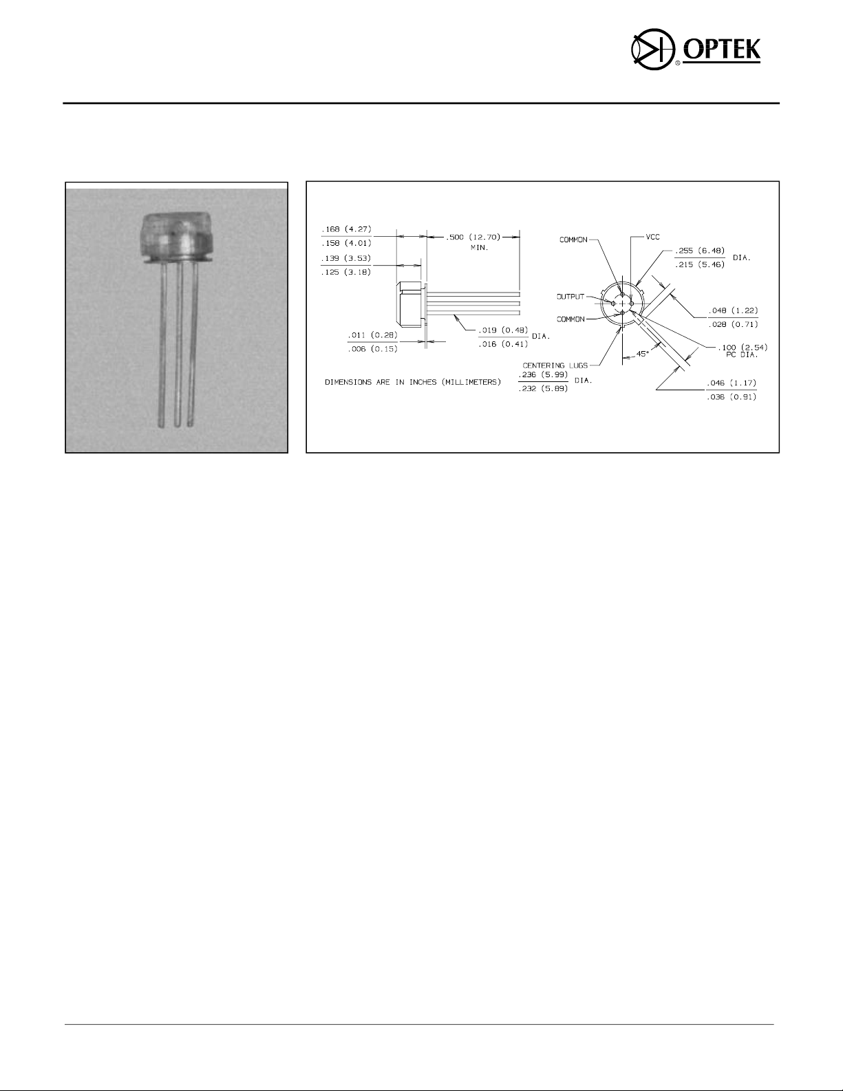
COM MON
OUT PUT
V
CC
Fea tures
• Electrically isolated plastic cap
package
• Designed to self align in the 0.228
diameter bore of standard fiber optic
receptacles
• Press fit simplifies component
installation
• Optimized for fiber optic applications
using 50 to 200 micron fiber
De scrip tion
The output of the receiver is an analog,
low impedance, voltage source capable
of driving an amplifier or level translating
circuitry for use on various data formats
and data rates up to 35 MBaud.
The receiver is comprised of a high
speed, low noise, photodiode coupled to
a transimpedance amplifier which
produces an output voltage proportional
to the input light amplitude. This hybrid
approach solves many of the problems of
high speed data link designs by placing a
pre-amplifier close to the photodiode.
The level amplification produced by the
transimpedance amplifier makes the
output signal much less susceptible to
interference which is a problem often
found at high data rates and in high EMI
environments.
Ab so lute Maxi mum Rat ings (TA = 25o C un less oth er wise noted)
Stor age Tem pera ture. . . . . . . . . . . . . . . . . . . . . . . . . . . . . . . . . . . . -55o C to +115o C
Op er at ing Tem pera ture . . . . . . . . . . . . . . . . . . . . . . . . . . . . . . . . . . . -40o C to +85o C
Lead Sol der ing Tem pera ture (for 10 sec.). . . . . . . . . . . . . . . . . . . . . . . . . . . . . 260o C
Sup ply Volt age . . . . . . . . . . . . . . . . . . . . . . . . . . . . . . . . . . . . . . . . . . . . . -0.5 to 7.0 V
Op tek Tech nol ogy, Inc. 1215 W. Crosby Road Car roll ton, Texas 75006 (972) 323- 2200 Fax (972) 323- 2396
8-102
Page 2
Type OPF540
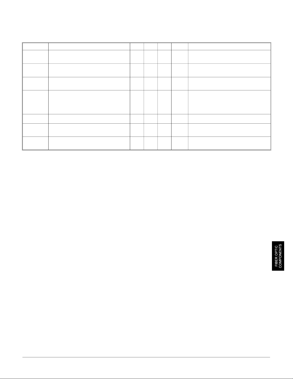
Elec tri cal Char ac ter is tics (TA = 25o C un less oth er wise noted)
4.75 ≤ VCC ≤ 5.25, R
= 511 Ω, Fi ber Sizes ≤ 100 Mi crons, N.A. ≤ 0.35
LOAD
SYM BOL PA RAME TERS MIN TYP MAX UNITS TEST CON DI TIONS
R
P
V
NO
P
N
P
R
I
CC
tr, t
PWD
Responsivity
RMS Output Noise Voltage
Equivalent Optical Noise Input Power
Peak Input Power
Power Supply Current
Rise Time, Fall Time (10% to 90%)
f
Pulse Width Distortion
6.5
9.3
5.8
0.30
-44.9
0.032
3.4 6.0 mA
14 19.5 ns
12.5
mV/µW
14.1
mV/µW
0.36
0.43mVmV
-40.9
0.082
-13.2
48
-14.7
34
2 ns
at 840 nm
at 840 nm, -40o C ≤ TA ≤ +85o C
PR = 0 µW
PR = 0 µW, -40o C ≤ TA ≤ +85o C
dBm
µW
dBm
TA = 25o C
TA = 25o C
µW
dBm
-40o C ≤ TA ≤ +85o C
µW
-40o C ≤ TA ≤ +85o C
R
= ∞
LOAD
PR = 10 µW Peak, R
C
= 13 pF
LOAD
PR = 40 µW Peak, R
C
= 13 pF
LOAD
LOAD
LOAD
= 511 Ω,
= 511 Ω,
Op tek re serves the right to make changes at any time in or der to im prove de sign and to sup ply the best prod uct pos si ble.
Op tek Tech nol ogy, Inc. 1215 W. Crosby Road Car roll ton, Texas 75006 (972)323- 2200 Fax (972)323- 2396
8-103
 Loading...