

Page 1

Prod uct Bul le tin OPB916
November 2000
Photologic Slotted Op ti cal Switches
Type OPB916 Series
[30.73]
1.21
[24.38]
.96
[2.54]
.10
[12.19]
.48
[3.18]
2X R .125
[14.99 0.38]
±
.590 ± .015
[5.08]
.20
[16.51]
.650 REF
[609.6]
24.0 MIN
[1.4 ± 0.51]
.055 ± .02
Fea tures
Choice of output configuration
•
24” min 26 AWG wires
•
• Low power consumption
[1.02]
4X R .125
[3.18]
2X .125
NOTE 6
OPTICAL C
[4.95]
.195
[3.81]
.15
L
WIRE COLOR
WHITE
BLUE
GREEN
RED
BLACK
[6.48]
.255
[19.30]
.760
WIRE: 26 AWG, 7 STRAND
PVC INSUL., UL RATED
IDENTITY
COLLECTOR
OUTPUT
EMITTER
ANODE
CATHODE
[3.18]
.125
De scrip tion
The OPB916 consists of an infrared
emitting diode and a Photologic photo
integrated circuit mounted in an opaque
housing with clear windows for dust
protection. The deep slot allows for a
longer reach of the optical path from the
mounting plane, .650” (16.51 mm).
Internal apertures are .010” x 0.06” for
the Photologic’s “S side” and .050” x
0.06” for the LED, “E side”. Two logic
states and two electrical output types are
available.
Custom electrical, wire or cabling are
available. Contact your local
representative or Optek for more
information.
Visit our website at www.optekinc.com
or email us at [email protected]
[ 8.89 ± 0.51]
.35 ± .02
[ 8.13 ± 0.51]
.32 ± .02
[ 7.62 ]
.30 REF
DIMENSIONS ARE IN INCHES [MILLIMETERS]
TOLERANCE ± .010 [0.25]
Ab so lute Maxi mum Rat ings (TA = 25o C un less oth er wise noted)
Sup ply Volt age VCC (Not to ex ceed 3 sec.) .............................. 18 V
Stor age and Op er ating Tem per a ture Range.................... -40° C to +80° C
In put Di ode Power Dis si pa tion ................................... 100 mW
Out put Photologic Power Dis si pa tion .............................. 90 mW
Volt age at Out put Lead (Open Col lec tor Out put) .......................... 35 V
Di ode For ward D.C. Cur rent ........................................ 50 mA
Di ode Re verse D.C. Volt age .......................................... 2 V
NOTES:
(1) De rate lin early 1.67 mW/° C above 25° C.
(2) De rate lin early 2.67 mW/° C above 70° C.
(3) Clear dust protection.
(4) Normal application would be with light source blocked, simulated by IF = 0 mA.
(5) All parameters tested using pulse technique.
PRECAUTIONS: Exposure of the plastic body to chlorinated hydrocarbons and ketones such
as thread lock and instant adhesive products will degrade the plastic body. Cleaning agents
methanol and isopropanol are recommended. Spray or wipe do not submerge.
(1)
(2)
Op tek Tech nol ogy, Inc. 1215 W. Crosby Road Car roll ton, Texas 75006 (972) 323- 2200 Fax (972) 323- 2396
33
Page 2

Type OPB916 Series
PART NUMBER GUIDE
Optek
Assembly
O P B 9 1 6 X X X
Photologic
Photo Integrated
Circuit
Optical Center
Line .90”
Schematics
OPB916B
Anode
(Red)
BUFFER WITH 10K PULL-UP RESISTOR
Electrical Specification Variations
B - Buffered with 10K Ω pull-up
BOC - Buffered Open-Collector Output
I - Inverted with 10K Ω pull-up
IOC - Inverted Open-Collector Output
OPB916I
VREG
AMP
V
CC
(White)
OUTPUT
(Blue)
Anode
(Red)
INVERTER WITH 10K PULL-UP RESISTOR
VREG
AMP
CC
V
(White)
OUTPUT
(Blue)
Cathode
(Black)
Anode
(Red)
Cathode
(Black)
LIGHT ON - OUTPUT HIGH
BUFFER OPEN COLLECTOR
VREG
AMP
LIGHT ON - OUTPUT HIGH
GROUND
(Green)
CC
V
(White)
OUTPUT
(Blue)
GROUND
(Green)
Cathode
(Black)
Anode
(Red)
Cathode
(Black)
LIGHT ON - OUTPUT LOW
OPB916OCIOPB916BOC
INVERTER OPEN COLLECTOR
VREG
AMP
LIGHT ON - OUTPUT LOW
GROUND
(Green)
V
CC
(White)
OUTPUT
(Blue)
GROUND
(Green)
Optek Tech nol ogy, Inc. 1215 W. Crosby Road Carrollton, Texas 75006 (972)323-2200 Fax (972)323-2396
35
Page 3
Type OPB916 Series
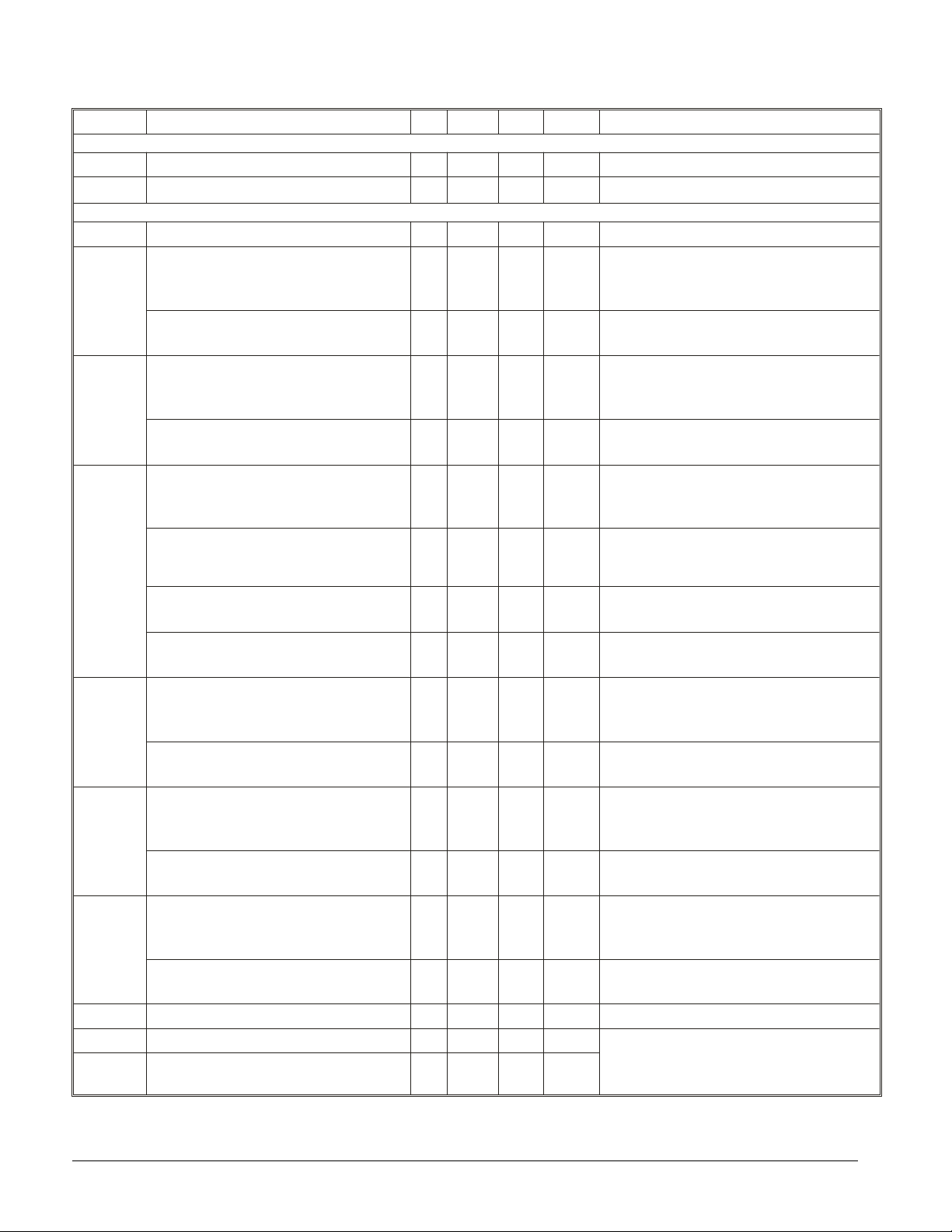
Elec tri cal Char ac ter is tics (TA = 25o C un less oth er wise noted)
SYM BOL PA RAME TER MIN TYP MAX UNITS TEST CON DI TIONS
In put Di ode
V
Phototransistor
V
I
CCL
Forward Voltage 1.30 1.80 V IF = 20 mA
F
I
Reverse Current
R
Operating D.C. Supply Voltage 4.5 16.0 V
CC
100
µA
Low Level Supply Current:
OPB916B and OPB916BOC 7.0 mA
OPB916I and OPB916IOC
7.0 mA
VR = 2 V
VCC = 16 V, IF = 0 mA
No Output Load
VCC = 16 V, IF = 10 mA
No Output Load
(4)
I
CCH
V
V
I
High Level Supply Current:
OPB916B and OPB916BOC 6.0 mA
OPB916I and OPB916IOC
Low Level Output Voltage:
OPB916B
OPB916BOC
OL
OPB916I
OPB916IOC
Low Level Output Voltage:
OPB916B 2.4
OH
OPB916I
2.4
v
-1.5
cc
v
-1.5 V
cc
High Level Output Current:
OPB916BOC 1.0 14
OH
OPB916IOC
1.0 14 µA
6.0 mA
0.4 V
0.4 V
0.4 V
0.4 V
V
µA
VCC = 16 V, IF = 10 mA
No Output Load
VCC = 16 V, IF = 0 mA
(4)
No Output Load
VCC = 4.5 to 16 V, IF = 0 mA
(4)
No Output Load
VCC = 4.5 to 16 V, IF = 0 mA
(4)
, IOL = 16
mA
No Output Load
VCC = 4.5 to 16 V, IF = 10 mA
No Output Load
VCC = 4.5 to 16 V, IF = 10 mA, IOL = 16 mA
No Output Load
VCC = 4.5 to 16 V, IF = 10 mA
No Output Load
VCC = 4.5 to16 V, IF = 0 mA
(4),
No Output Load
VCC = 4.5 V, VOH = 30 V, IF = 10 mA
VCC = 4.5 V, VOH = 30 V, IF = 0 mA
IF(+)
LED Positive-Going Threshold
Current:
OPB916B and OPB916I
OPB916BOC and OPB916IOC
5 10 mA
5 10 mA
VCC = 5 V
No Output Load
VCC = 5 V, IOL = 16 mA
No Output Load
IF(+)/IF(-) Hysteresis 1.5
tr, tfRise Time, Fall Time 50 ns VCC = 5 V, IF = 0 or 10 mA
t
PLH
Propagation Delay Low-High &
, t
PHL
High-Low
3.0
RL = 300 Ω to 5 V, CL = 50 pF
µs
Op tek re serves the right to make changes at any time in or der to im prove de sign and to sup ply the best prod uct pos si ble.
Op tek Tech nol ogy, Inc. 1215 W. Crosby Road Car roll ton, Texas 75006 (972)323- 2200 Fax (972)323- 2396
34
 Loading...