

Datasheet OPA2241UA-2K5, OPA251UA-2K5, OPA241UA, OPA4241PA, OPA4251UA Datasheet (Burr Brown)
...Page 1
®
OPA241
OPA4251
OPA241
OPA2241
OPA4241
OPA4241
Single-Supply,
OPERATIONAL AMPLIFIERS
OPA241 Family optimized for +5V supply.
OPA251 Family optimized for ±15V supply.
FEA TURES
●
Micro
POWER: IQ = 25µA
● SINGLE-SUPPLY OPERATION
● RAIL-TO-RAIL OUTPUT (within 50mV)
● WIDE SUPPLY RANGE
Single Supply: +2.7V to +36V
Dual Supply: ±1.35V to ±18V
● LOW OFFSET VOLTAGE: ±250µV max
● HIGH COMMON-MODE REJECTION: 124dB
● HIGH OPEN-LOOP GAIN: 128dB
● SINGLE, DUAL, AND QUAD
APPLICATIONS
● BATTERY OPERATED INSTRUMENTS
● PORTABLE DEVICES
● MEDICAL INSTRUMENTS
● TEST EQUIPMENT
OPA2251
OPA251
OPA2251
OPA4251
Micro
POWER
DESCRIPTION
The OPA241 series and OPA251 series are specifically
designed for battery powered, portable applications. In addition to very low power consumption (25µA), these amplifiers feature low offset voltage, rail-to-rail output swing, high
common-mode rejection, and high open-loop gain.
The OPA241 series is optimized for operation at low power
supply voltage while the OPA251 series is optimized for
high power supplies. Both can operate from either single
(+2.7V to +36V) or dual supplies (±1.35V to ±18V). The
input common-mode voltage range extends 200mV below
the negative supply—ideal for single-supply applications.
They are unity-gain stable and can drive large capacitive
loads. Special design considerations assure that these products are easy to use. High performance is maintained as the
amplifiers swing to their specified limits. Because the initial
offset voltage (±250µV max) is so low, user adjustment is
usually not required. However, external trim pins are provided for special applications (single versions only).
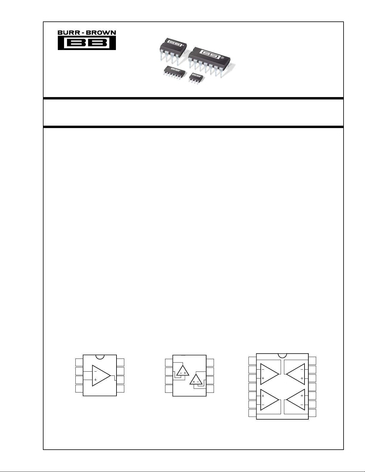
The OPA241 and OPA251 (single versions) are available
in standard 8-pin DIP and SO-8 surface-mount packages.
The OPA2241 and OPA2251 (dual versions) come in 8-pin
DIP and SO-8 surface-mount packages. The OPA4241 and
OPA4251 (quad versions) are available in 14-pin DIP and
SO-14 surface-mount packages. All are fully specified
from –40°C to +85°C and operate from –55°C to +125°C.
OPA241, OPA251
Offset Trim
International Airport Industrial Park • Mailing Address: PO Box 11400, Tucson, AZ 85734 • Street Address: 6730 S. Tucson Blvd., Tucson, AZ 85706 • Tel: (520) 746-1111 • Twx: 910-952-1111
Internet: http://www.burr-brown.com/ • FAXLine: (800) 548-6133 (US/Canada Only) • Cable: BBRCORP • Telex: 066-6491 • FAX: (520) 889-1510 • Immediate Product Info: (800) 548-6132
© 1997 Burr-Brown Corporation PDS-1406B Printed in U.S.A. October, 1998
–In
+In
1
2
3
V–
4
8-Pin DIP, SO-8
8
7
6
5
NC
V+
Output
Offset Trim
Out A
–In A
+In A
OPA2241, OPA2251
1
2
3
V–
4
A
B
8-Pin DIP, SO-8
1
V+
8
Out B
7
–In B
6
+In B
5
Out A
–In A
+In A
V+
+In B
–In B
Out B
OPA4241, OPA4251
1
2
AD
3
4
5
BC
6
7
14-Pin DIP, SO-14
OPA241, 2241, 4241
OPA251, 2251, 4251
Out D
14
–In D
13
+In D
12
V–
11
+In C
10
–In C
9
Out C
8
®
Page 2
SPECIFICATIONS: VS = 2.7V to 5V
At TA = +25°C, RL = 100kΩ connected to VS/2, unless otherwise noted.
Boldface limits apply over the specified temperature range, T
PARAMETER CONDITION MIN TYP
OFFSET VOLTAGE
Input Offset Voltage V
T
= –40°C to +85°C ±100 ±400 ±130 µV
A
vs Temperature dV
vs Power Supply PSRR V
T
= –40°C to +85°C VS = 2.7V to 36V 30 ✻ µV/V
A
Channel Separation (dual, quad) 0.3 ✻ µV/V
INPUT BIAS CURRENT
Input Bias Current
T
= –40°C to +85°C –25 nA
A
Input Offset Current I
T
= –40°C to +85°C ±2 nA
A
(2)
OS
/dT TA = –40°C to +85°C ±0.4 ±0.6 µV/°C
OS
I
B
OS
NOISE
Input Voltage Noise, f = 0.1Hz to 10Hz 1 ✻ µVp-p
Input Voltage Noise Density, f = 1kHz e
Current Noise Density, f = 1kHz i
n
n
INPUT VOLTAGE RANGE
Common-Mode Voltage Range V
Common-Mode Rejection Ratio CMRR V
T
= –40°C to +85°C V
A
CM
INPUT IMPEDANCE
Differential 10
Common-Mode 10
OPEN-LOOP GAIN
Open-Loop Voltage Gain A
T
= –40°C to +85°C
A
T
= –40°C to +85°C
A
= 100kΩ, VO = (V–)+100mV to (V+)–100mV
OLRL
RL = 100kΩ, VO = (V–)+100mV to (V+)–100mV
RL = 10kΩ, VO = (V–)+200mV to (V+)–200mV
RL = 10kΩ, VO = (V–)+200mV to (V+)–200mV
FREQUENCY RESPONSE
Gain-Bandwidth Product GBW 35 ✻ kHz
Slew Rate SR V
Overload Recovery Time V
OUTPUT
Voltage Output Swing from Rail
T
= –40°C to +85°C RL = 100kΩ to VS/2, A
A
T
= –40°C to +85°C RL = 10kΩ to VS/2, A
A
Short-Circuit Current I
Single Versions –24/+4 ✻ mA
(3)
V
RL = 100kΩ to VS/2, A
O
R
L
R
SC
Dual, Quad Versions –30/+4 ✻ mA
Capacitive Load Drive C
LOAD
POWER SUPPLY
Specified Voltage Range V
Operating Voltage Range T
Quiescent Current (per amplifier) I
T
= –40°C to +85°C IO = 0 ±36 µA
A
S
Q
TEMPERATURE RANGE
Specified Range –40 +85 ✻✻°C
Operating Range –55 +125 ✻✻°C
Storage Range –55 +125 ✻✻°C
Thermal Resistance
8-Pin DIP 100 ✻ °C/W
θ
JA
SO-8 Surface Mount 150 ✻ °C/W
14-Pin DIP 80 ✻ °C/W
SO-14 Surface Mount 100 ✻ °C/W
✻ Specifications the same as OPA241UA, PA.
NOTES: (1) V
output and power supply rails.
= +5V. (2) The negative sign indicates input bias current flows out of the input terminals. (3) Output voltage swings are measured between the
S
The information provided herein is believed to be reliable; however, BURR-BROWN assumes no responsibility for inaccuracies or omissions. BURR-BROWN assumes
no responsibility for the use of this information, and all use of such information shall be entirely at the user’s own risk. Prices and specifications are subject to change
without notice. No patent rights or licenses to any of the circuits described herein are implied or granted to any third party. BURR-BROWN does not authorize or warrant
any BURR-BROWN product for use in life support devices and/or systems.
= –40°C to +85°C.
A
OPA241UA, PA OPA251UA, PA
OPA2241UA, PA OPA2251UA, PA
OPA4241UA, PA OPA4251UA, PA
(1)
MAX MIN TYP
(1)
±50 ±250 ±100 µV
= 2.7V to 36V 3 30 ✻✻µV/V
S
–4 –20 ✻ nA
±0.1 ±2 ✻ nA
45 ✻ nV/√Hz
40 ✻ fA/√Hz
= –0.2V to (V+) –0.8V 80 106 ✻ dB
–0.2
CM
= 0V to (V+) –0.8V 80 dB
CM
(V+) –0.8
7
|| 2 ✻ Ω || pF
9
|| 4 ✻ Ω || pF
100 120 ✻ dB
100 dB
100 120 ✻ dB
100 dB
= 5V, G = 1 0.01 ✻ V/µs
S
• G = V
IN
= 100kΩ to VS/2, A
= 10kΩ to VS/2, A
L
S
≥ 70dB 50 ✻ mV
OL
≥ 100dB 75 100 ✻ mV
OL
≥ 100dB 100 mV
OL
≥ 100dB 100 200 ✻ mV
OL
≥ 100dB 200 mV
OL
60 ✻ µs
See Typical Curve ✻
= –40°C to +85°C +2.7 +36 ✻✻V
+2.7 to +5
A
IO = 0 ±25 ±30 ✻ µA
✻ V
MAX UNITS
V
®
OPA241, 2241, 4241
OPA251, 2251, 4251
2
Page 3
SPECIFICATIONS: VS = ±15V
At TA = +25°C, RL = 100kΩ connected to ground, unless otherwise noted.
Boldface limits apply over the specified temperature range, T
PARAMETER CONDITION MIN TYP MAX MIN TYP MAX UNITS
OFFSET VOLTAGE
Input Offset Voltage V
T
= –40°C to +85°C ±150 ±100 ±300 µV
A
vs Temperature dV
vs Power Supply PSRR V
T
= –40°C to +85°C VS = ±1.35V to ±18V ✻ 30 µV/V
A
Channel Separation (dual, quad) ✻ 0.3 µV/V
INPUT BIAS CURRENT
Input Bias Current
T
= –40°C to +85°C –25 nA
A
Input Offset Current I
T
= –40°C to +85°C ±2 nA
A
(1)
OS
/dT TA = –40°C to +85°C ±0.6 ±0.5 µV/°C
OS
I
B
OS
NOISE
Input Voltage Noise, f = 0.1Hz to 10Hz ✻ 1 µVp-p
Input Voltage Noise Density, f = 1kHz e
Current Noise Density, f = 1kHz i
n
n
INPUT VOLTAGE RANGE
Common-Mode Voltage Range V
Common-Mode Rejection Ratio CMRR V
T
= –40°C to +85°C V
A
CM
INPUT IMPEDANCE
Differential ✻ 10
Common-Mode ✻ 10
OPEN-LOOP GAIN
Open-Loop Voltage Gain A
T
= –40°C to +85°C
A
T
= –40°C to +85°C
A
= 100kΩ, VO = –14.75V to +14.75V
OLRL
RL = 100kΩ, VO = –14.75V to +14.75V
RL = 20kΩ, VO = –14.7V to +14.7V
RL = 20kΩ, VO = –14.7V to +14.7V
FREQUENCY RESPONSE
Gain-Bandwidth Product GBW ✻ 35 kHz
Slew Rate SR G = 1 ✻ 0.01 V/µs
Overload Recovery Time V
OUTPUT
Voltage Output Swing from Rail
T
= –40°C to +85°C RL = 100kΩ, A
A
T
= –40°C to +85°C RL = 20kΩ, A
A
Short-Circuit Current I
Single Versions ✻ –21/+4 mA
(2)
V
O
SC
Dual Versions ✻ –50/+4 mA
Capacitive Load Drive C
LOAD
POWER SUPPLY
Specified Voltage Range V
Operating Voltage Range T
Quiescent Current (per amplifier) I
T
= –40°C to +85°C IO = 0 ±45 µA
A
S
Q
TEMPERATURE RANGE
Specified Range ✻✻–40 +85 °C
Operating Range ✻✻–55 +125 °C
Storage Range ✻✻–55 +125 °C
Thermal Resistance
8-Pin DIP ✻ 100 °C/W
θ
JA
SO-8 Surface Mount ✻ 150 °C/W
14-Pin DIP ✻ 80 °C/W
SO-14 Surface Mount ✻ 100 °C/W
✻ Specifications the same as OPA251UA, PA.
NOTES: (1) The negative sign indicates input bias current flows out of the input terminals. (2) Output voltage swings are measured between the output and
power supply rails.
= –40°C to +85°C.
A
OPA241UA, PA OPA251UA, PA
OPA2241UA, PA OPA2251UA, PA
OPA4241UA, PA OPA4251UA, PA
±100 ±50 ±250 µV
= ±1.35V to ±18V ✻✻ 330µV/V
S
✻ –4 –20 nA
✻ ±0.1 ±2nA
✻ 45 nV/√Hz
✻ 40 fA/√Hz
(V–) –0.2 (V+) –0.8
= –15.2V to 14.2V ✻ 100 124 dB
CM
= –15V to 14.2V 100 dB
CM
7
|| 2 Ω || pF
9
|| 4 Ω || pF
✻ 100 128 dB
100 dB
✻ 100 128 dB
100 dB
• G = V
IN
RL = 100kΩ, A
R
= 100kΩ, A
L
R
= 20kΩ, A
L
S
≥ 70dB ✻ 50 mV
OL
≥ 100dB ✻ 75 250 mV
OL
≥ 100dB 250 mV
OL
≥ 100dB ✻ 100 300 mV
OL
≥ 100dB 300 mV
OL
✻ 60 µs
✻ See Typical Curve
✻ ±15 V
= –40°C to +85°C ✻✻±1.35 ±18 V
A
IO = 0 ✻ ±27 ±38 µA
V
3
OPA251, 2251, 4251
OPA241, 2241, 4241
®
Page 4

ABSOLUTE MAXIMUM RATINGS
Supply Voltage, V+ to V– .................................................................... 36V
Input Voltage
Output Short Circuit
Operating Temperature .................................................. –55°C to +125°C
Storage Temperature .....................................................–55°C to +125°C
Junction Temperature...................................................................... 150°C
Lead Temperature (soldering, 10s) ................................................. 300 °C
NOTES: (1) Stresses above these ratings may cause permanent damage.
(2) Input terminals are diode-clamped to the power supply rails. Input signals
that can swing more that 0.5V beyond the supply rails should be currentlimited to 5mA or less. (3) One amplifier per package.
(2)
.................................................. (V–) –0.5V to (V+) +0.5V
to Ground
(3)
............................................ Continuous
(1)
ELECTROSTATIC
DISCHARGE SENSITIVITY
This integrated circuit can be damaged by ESD. Burr-Brown
recommends that all integrated circuits be handled with
appropriate precautions. Failure to observe proper handling
and installation procedures can cause damage.
ESD damage can range from subtle performance degradation to complete device failure. Precision integrated circuits
may be more susceptible to damage because very small
parametric changes could cause the device not to meet its
published specifications.
PACKAGE/ORDERING INFORMATION
PRODUCT VOLTAGE RANGE PACKAGE NUMBER
SPECIFIED VOLTAGE DRAWING TEMPERATURE
OPA241 SERIES
Single
OPA241PA 2.7V to 5V 2.7V to 36V 8-Pin DIP 006 –40°C to +85°C
OPA241UA 2.7V to 5V 2.7V to 36V SO-8 Surface Mount 182 –40°C to +85°C
Dual
OPA2241PA 2.7V to 5V 2.7V to 36V 8-Pin DIP 006 –40°C to +85°C
OPA2241UA 2.7V to 5V 2.7V to 36V SO-8 Surface Mount 182 –40°C to +85°C
Quad
OPA4241PA 2.7V to 5V 2.7V to 36V 14-Pin DIP 010 –40°C to +85°C
OPA4241UA 2.7V to 5V 2.7V to 36V SO-14 Surface Mount 235 –40°C to +85°C
OPA251 SERIES
Single
OPA251PA ±15V 2.7V to 36V 8-Pin DIP 006 –40°C to +85°C
OPA251UA ±15V 2.7V to 36V SO-8 Surface Mount 182 –40°C to +85°C
Dual
OPA2251PA ±15V 2.7V to 36V 8-Pin DIP 006 –40°C to +85°C
OPA2251UA ±15V 2.7V to 36V SO-8 Surface Mount 182 –40°C to +85°C
Quad
OPA4251PA ±15V 2.7V to 36V 14-Pin DIP 010 –40°C to +85°C
OPA4251UA ±15V 2.7V to 36V SO-14 Surface Mount 235 –40°C to +85°C
NOTE: (1) For detailed drawing and dimension table, please see end of data sheet, or Appendix C of Burr-Brown IC Data Book.
OPERATING PACKAGE SPECIFICATION
(1)
RANGE
®
OPA241, 2241, 4241
OPA251, 2251, 4251
4
Page 5

TYPICAL PERFORMANCE CURVES
At TA = +25°C, and RL = 100kΩ connected to VS/2 (ground for VS = ±15V), unless otherwise noted.
Curves apply to OPA241 and OPA251 unless specified.
160
140
120
100
80
60
40
Voltage Gain (dB)
20
0
–20
OPEN-LOOP GAIN/PHASE vs FREQUENCY
G
VS = ±15V
V
= +5V
S
0.01 0.1
1 10 100 1k 10k 100k
Frequency (Hz)
180
160
140
120
100
Φ
80
Phase (°)
60
40
20
0
140
120
100
80
60
40
20
Power Supply Rejection Ratio (dB)
0
POWER SUPPLY and COMMON-MODE
REJECTION RATIO vs FREQUENCY
VS = ±15V
VS = ±5V
CMRR
+PSRR
–PSRR
0.1 1 10 100 1k 10k 100k
Frequency (Hz)
140
130
120
110
100
90
Channel Separation (dB)
80
70
30
28
26
24
Quiescent Current (µA)
CHANNEL SEPARATION vs FREQUENCY
Dual and quad devices.
G = 1, all channels.
Quad measured channel
A to D or B to C—other
combinations yield improved
rejection.
10010 1k 10k 100k
QUIESCENT CURRENT vs SUPPLY VOLTAGE
Per Amplifier
Frequency (Hz)
INPUT VOLTAGE AND CURRENT
NOISE SPECTRAL DENSITY vs FREQUENCY
Current Noise
Voltage Noise
0.1 1 10 100 1k 10k
Frequency (Hz)
QUIESCENT CURRENT vs TEMPERATURE
Per Amplifier
VS = ±15V
VS = +5V
Voltage Noise (nV/÷Hz)
Quiescent Current (µA)
1k
100
10
40
35
30
25
20
1k
100
Current Noise (fA/√Hz)
10
22
0 5 10 15 20 25 30 35 40
Total Supply Voltage (V)
15
–75 –50 –25 0 25 50 75 100 125
Temperature (°C)
5
OPA251, 2251, 4251
OPA241, 2241, 4241
®
Page 6

TYPICAL PERFORMANCE CURVES (CONT)
At TA = +25°C, and RL = 100kΩ connected to VS/2 (ground for VS = ±15V), unless otherwise noted.
Curves apply to OPA241 and OPA251 unless specified.
INPUT BIAS CURRENT vs TEMPERATURE
–6
–4
I
B
–2
I
0
Input Bias Current (nA)
OS
2
–75 –50 –25 0 25 50 75 100 125
Temperature (°C)
SHORT-CIRCUIT CURRENT vs TEMPERATURE
50
45
–I
40
35
30
25
20
15
10
Short-Circuit Current (mA)
SC
Single Versions
Dual, Quad Versions
+ISC, VS = +5V, ±15V (all versions)
5
0
–75 –50 –25 0 25 50 75 100 125
Temperature (°C)
VS = ±15V
VS = +5V
VS = +5V
VS = ±15V
INPUT BIAS CURRENT
–5
–4
–3
–2
Input Bias Current (nA)
–1
0
0 5 10 15 20 25 30
140
120
100
80
60
40
20
Common-Mode Rejection (dB)
0
–75 –50 –25 0 25 50 75 100 125
vs INPUT COMMON-MODE VOLTAGE
I
B
I
OS
Common-Mode Voltage (V)
COMMON-MODE REJECTION vs TEMPERATURE
VS = ±15V
VS = +2.7V, +5V
= (V–) –0.2V to (V+) –0.8V
V
CM
V
= (V–) –0.1V to (V+) –0.8V
CM
V
= (V–) to (V+) –0.8V
CM
Temperature (°C)
OPEN-LOOP GAIN AND POWER
140
130
120
, PSR (dB)
OL
A
110
100
–75 –50 –25 0 25 50 75 100 125
SUPPLY REJECTION vs TEMPERATURE
RL = 20kΩ, 100kΩ
RL = 10kΩ
AOL, VS = ±15V
A
, VS = +5V
OL
Temperature (°C)
®
OPA241, 2241, 4241
PSRR
RL = 100kΩ
OPA251, 2251, 4251
(V+)
(V+) –0.1V
(V+) –0.2V
(V+) –0.3V
(V–) +0.3V
(V–) +0.2V
Output Voltage Swing (V)
(V–) +0.1V
(V–)
0.1 ±1 ±10
6
OUTPUT VOLTAGE SWING vs OUTPUT CURRENT
T = +25°C
T = –55°C
T = +125°C
T = +125°C
T = +25°C, –55°C
Output Current (mA)
Page 7

TYPICAL PERFORMANCE CURVES (CONT)
MAXIMUM OUTPUT VOLTAGE vs FREQUENCY
100k100 1k 10k
Frequency (Hz)
10
30
25
20
15
10
5
0
Maximum Output Voltage (Vp-p)
Maximum output
voltage without
slew rate-induced
distortion.
VS = 2.7V
VS = +5V
VS = ±15V
At TA = +25°C, and RL = 100kΩ connected to VS/2 (ground for VS = ±15V), unless otherwise noted.
Curves apply to OPA241 and OPA251 unless specified.
140
130
OPEN-LOOP GAIN vs OUTPUT VOLTAGE SWING
VS = ±15V
RL = 20kΩ
RL = 100kΩ
VS = +5V
120
VS = +2.7V
110
100
Open-Loop Gain (dB)
90
80
500 400 300 200 100 0
Output Voltage Swing from Rail (mV)
OPA241 SERIES OFFSET VOLTAGE
30
Typical production
distribution of
25
packaged units.
Singles, duals,
20
and quads included.
15
10
Percent of Amplifiers (%)
5
0
–225
PRODUCTION DISTRIBUTION
–200
–175
–150
–125
–100
RL = 10kΩ
0
–50
–25
255075
–75
Offset Voltage (µV)
VS = +5V
100
125
150
175
200
225
OPA241 SERIES OFFSET VOLTAGE DRIFT
20
= +5V
V
S
18
16
14
12
10
8
6
4
Percent of Amplifiers (%)
2
0
0 0.1 0.2 0.3 0.4 0.5 0.6 0.7 0.8 0.9 1.0 1.1 1.2 1.3
PRODUCTION DISTRIBUTION
Typical production distribution
of packaged units. Singles,
duals, and quads included.
Offset Voltage (µV/°C)
30
25
20
15
10
Percent of Amplifiers (%)
5
0
OPA251 SERIES OFFSET VOLTAGE
PRODUCTION DISTRIBUTION
VS = ±15V
–75
–50
–225
–200
–175
–150
–125
–25
–100
Offset Voltage (µV)
Typical production
distribution of
packaged units.
Singles, duals,
and quads included.
0
255075
100
125
150
175
200
225
OPA251 SERIES OFFSET VOLTAGE DRIFT
18
V
= ±15V
S
16
14
12
10
8
6
4
Percent of Amplifiers (%)
2
0
0
0.1
7
PRODUCTION DISTRIBUTION
Typical production distribution
of packaged units. Singles,
duals, and quads included.
0.2
0.3
0.4
0.5
0.6
0.7
0.8
0.9
Offset Voltage Drift (µV/°C)
OPA241, 2241, 4241
OPA251, 2251, 4251
1.0
1.1
1.2
1.3
1.4
1.5
1.6
1.7
1.8
1.9
2.0
®
Page 8

TYPICAL PERFORMANCE CURVES (CONT)
At TA = +25°C, and RL = 100kΩ connected to VS/2 (ground for VS ±15V), unless otherwise noted.
Curves apply to OPA241 and OPA251 unless specified.
25
VS = +5V
20
Per Amplifier
15
10
5
Percent of Amplifiers (%)
0
21
21.52222.52323.52424.52525.52626.52727.52828.52929.5
SMALL-SIGNAL STEP RESPONSE
V
= +5V, G = +1, RL = 100kΩ, CL = 100pF
S
QUIESCENT CURRENT
PRODUCT DISTRIBUTION
Typical production
distribution of
packaged units.
Singles, duals,
and quads included.
Quiescent Current (µA)
OPA241
QUIESCENT CURRENT
35
VS = ±15V
30
25
20
15
10
Percent of Amplifiers (%)
5
0
30
2223242526272829303132333435363738
V
= +5V, G + 1, RL = 100kΩ, CL = 100pF
S
PRODUCTION DISTRIBUTION
Typical production distribution
of packaged units. Singles,
duals, and quads included.
Per Amplifier
Quiescent Current (µA)
OPA241
LARGE-SIGNAL STEP RESPONSE
50mV/div
200µs/div
SMALL-SIGNAL STEP RESPONSE
V
= ±15V, G = +1, RL = 100kΩ, CL = 500pF
S
50mV/div
OPA251
200µs/div
0.5V/div
200µs/div
OPA251
LARGE-SIGNAL STEP RESPONSE
VS = ±15V, G = +1, RL = 100kΩ, CL = 500pF
2V/div
2ms/div
®
OPA241, 2241, 4241
OPA251, 2251, 4251
8
Page 9

APPLICATIONS INFORMATION
The OPA241 and OPA251 series are unity-gain stable and
suitable for a wide range of general purpose applications.
Power supply pins should be bypassed with 0.01µF ceramic
capacitors.
OPERATING VOLTAGE
The OPA241 series is laser-trimmed for low offset voltage
and drift at low supply voltage (VS = +5V). The OPA251
series is trimmed for ±15V operation. Both products operate
over the full voltage range (+2.7V to +36V or ±1.35V to
±18V) with some compromises in offset voltage and drift
performance. However, all other parameters have similar
performance. Key parameters are guaranteed over the specified temperature range, –40°C to +85°C. Most behavior
remains unchanged throughout the full operating voltage
range. Parameters which vary significantly with operating
voltage or temperature are shown in typical performance
curves.
Figures 2 and 3 show the regions where the OPA241 series
and OPA251 series have the potential for instability. As
shown, the unity gain configuration with low supplies is the
most susceptible to the effects of capacitive load. With VS =
+5V, G = +1, and I
= 0, operation remains stable with
OUT
load capacitance up to approximately 200pF. Increasing
supply voltage, output current, and/or gain significantly
improves capacitive load drive. For example, increasing the
supplies to ±15V and gain to 10 allows approximately
2700pF to be driven.
One method of improving capacitive load drive in the unity
gain configuration is to insert a resistor inside the feedback
loop as shown in Figure 4. This reduces ringing with large
capacitive loads while maintaining dc accuracy. For example, with VS = ±1.35V and RS = 5kΩ, the OPA241 series
and OPA251 series perform well with capacitive loads in
excess of 1000pF. Without the series resistor, capacitive
load drive is typically 200pF for these conditions. However,
this method will result in a slight reduction of output voltage
swing.
OFFSET VOLTAGE TRIM
As mentioned previously, offset voltage of the OPA241
series is laser-trimmed at +5V. The OPA251 series is trimmed
at ±15V. Because the initial offset is so low, user adjustment
is usually not required. However, the OPA241 and OPA251
(single op amp versions) provide offset voltage trim connections on pins 1 and 5. Offset voltage can be adjusted by
connecting a potentiometer as shown in Figure 1. This
adjustment should be used only to null the offset of the op
amp, not to adjust system offset or offset produced by the
signal source. Nulling offset could degrade the offset drift
behavior of the op amp. While it is not possible to predict the
exact change in drift, the effect is usually small.
V+
OPA241 and OPA251 (single op amps) only.
0.01µF
Use offset adjust pins only to null
7
offset voltage of op amp—see text.
OPA241
V–
6
5
1
100kΩ
Trim Range: ±2mV
(V–) = 0V for single-supply operation.
0.01µF
2
3
4
FIGURE 1. OPA241 and OPA251 Offset Voltage Trim
Circuit.
CAPACITIVE LOAD AND STABILITY
The OPA241 series and OPA251 series can drive a wide
range of capacitive loads. However, all op amps under
certain conditions may be unstable. Op amp configuration,
gain, and load value are just a few of the factors to consider
when determining stability.
100k
VS = +2.7V
= +5V
V
S
10k
1k
Capacitive Load (pF)
100
–1 –0.1 –0.01 0 0.01 0.1 1
G = –1
Sinking
G = +1
G = 10
Output Current (mA)
Operation above
selected gain curve
not recommended
Sourcing
FIGURE 2. Stability—Capacitive Load versus Output Cur-
rent for Low Supply Voltage.
100k
VS = ±15V
10k
1k
Capacitive Load (pF)
Sinking
100
–1 –0.1 –0.01 0 0.01 0.1 1
G = 10
G = +1
Output Current (mA)
Operation above
selected gain curve
not recommended
G = –1
Sourcing
FIGURE 3. Stability—Capacitive Load versus Output Cur-
rent for ±15V Supplies.
OPA241, 2241, 4241
9
OPA251, 2251, 4251
®
Page 10

R
S
OPA241
V
IN
5kΩ
V
OUT
C
L
FIGURE 4. Series Resistor in Unity Gain Configuration Improves Capacitive Load Drive.
R
H
10Ω
R
5
383kΩ
V+
A1
OPA241
Out
R
1
38.3kΩ
I
H
R
3
38.3kΩ
High-Side
Current Sense
–In
+In
To Load
= 10 • IH • R
V
O
H
V+ for A
, A
1
2
+
2.7V to ±15V
V– for A1, A
2
R
8
100kΩ
V+
–In
A2
R
10kΩ
6
R
10Ω
I
OPA241
+In
R
7
9.09kΩ
L
Optional for I
(R
L
V–
Current Sense
Cancellation
B
= R6 II R8)
7
Out
NOTE: Low and high-side sensing circuits can be used independently.
FIGURE 5. Low and High-Side Battery Current Sensing.
R
20kΩ
Low-Side
V–
4
R
2
19.1kΩ
R
and R4 divide down the
2
common-mode input to A1.
VO = 10 • IL • R
L
Common-mode range of A2
extends to V– for low-side sensing.
To Load
®
OPA241, 2241, 4241
OPA251, 2251, 4251
10
 Loading...