

Page 1
®
OPA27
OPA27
Ultra-Low Noise Precision
OPERATIONAL AMPLIFIERS
OPA27
OPA37
FEATURES
● LOW NOISE: 4.5nV/√Hz max at 1kHz
● LOW OFFSET: 100
● LOW DRIFT: 0.4
µV max
µV/°C
● HIGH OPEN-LOOP GAIN: 117dB min
● HIGH COMMON-MODE REJECTION:
100dB min
● HIGH POWER SUPPLY REJECTION:
94dB min
● FITS OP-07, OP-05, AD510, AD517
SOCKETS
DESCRIPTION
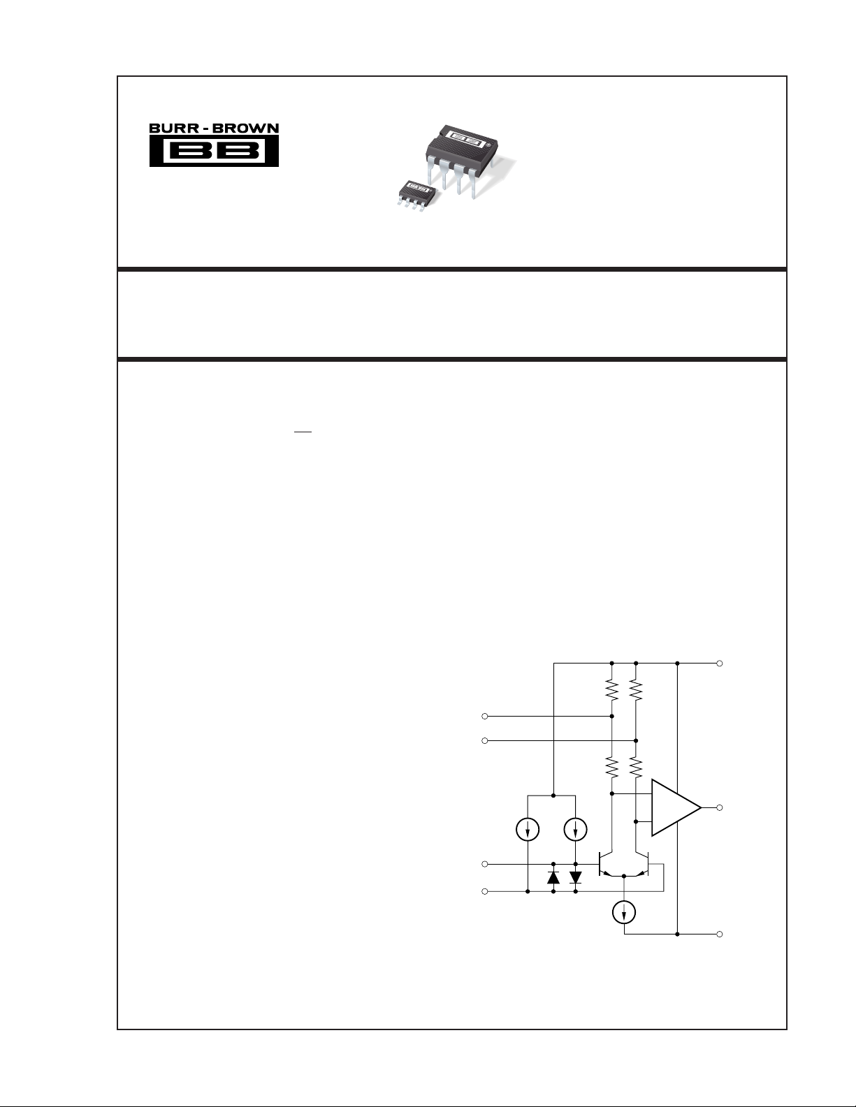
The OPA27/37 is an ultra-low noise, high precision
monolithic operational amplifier.
Laser-trimmed thin-film resistors provide excellent
long-term voltage offset stability and allow superior
voltage offset compared to common zener-zap techniques.
A unique bias current cancellation circuit allows bias
and offset current specifications to be met over the full
–55°C to +125°C temperature range.
The OPA27 is internally compensated for unity-gain
stability. The decompensated OPA37 requires a closedloop gain ≥ 5.
The Burr-Brown OPA27/37 is an improved replacement for the industry-standard OP-27/OP-37.
APPLICATIONS
● PRECISION INSTRUMENTATION
● DATA ACQUISITION
● TEST EQUIPMENT
● PROFESSIONAL AUDIO EQUIPMENT
● TRANSDUCER AMPLIFIER
● RADIATION HARD EQUIPMENT
8
Trim
1
Trim
2
–In
3
+In
7
6
4
+V
CC
Output
–V
CC
International Airport Industrial Park • Mailing Address: PO Box 11400, Tucson, AZ 85734 • Street Address: 6730 S. Tucson Blvd., Tucson, AZ 85706 • Tel: (520) 746-1111 • Twx: 910-952-1111
Internet: http://www.burr-brown.com/ • FAXLine: (800) 548-6133 (US/Canada Only) • Cable: BBRCORP • Telex: 066-6491 • FAX: (520) 889-1510 • Immediate Product Info: (800) 548-6132
®
© 1984 Burr-Brown Corporation PDS-466M Printed in U.S.A. March, 1998
1
OPA27, 37
Page 2
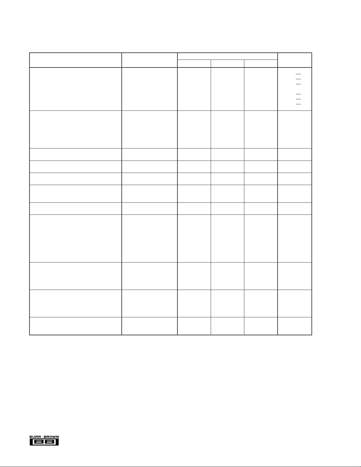
SPECIFICATIONS
At V
= ±15V and TA = +25°C, unless otherwise noted.
CC
OPA27/37G
PARAMETER CONDITIONS MIN TYP MAX UNITS
INPUT NOISE
Voltage, fO = 10Hz 3.8 8.0 nV/√Hz
Current,
OFFSET VOLTAGE
Input Offset Voltage ±25 ±100 µV
Average Drift
Long Term Stability
(6)
f
= 30Hz 3.3 5.6 nV/√Hz
O
f
= 1kHz 3.2 4.5 nV/√Hz
O
f
= 0.1Hz to 10Hz 0.09 0.25 µVp-p
B
(1)
fO = 10Hz 1.7 pA/√Hz
f
= 30Hz 1.0 pA/√Hz
O
f
= 1kHz 0.4 0.6 pA/√Hz
O
(2)
(3)
(4)
T
A MIN
to T
A MAX
±0.4 ±1.8
0.4 2.0 µV/mo
(6)
µV/°C
Supply Rejection ±V
= 4 to 18V 94 120 dB
CC
±V
= 4 to 18V ±1 ±20 µV/V
CC
BIAS CURRENT
Input Bias Current ±15 ±80 nA
OFFSET CURRENT
Input Offset Current 10 75 nA
IMPEDANCE
Common-Mode 2 || 2.5 GΩ || pF
VOLTAGE RANGE
Common-Mode Input Range ±11 ±12.3 V
Common-Mode Rejection V
OPEN-LOOP VOLTAGE GAIN, DC R
FREQUENCY RESPONSE
Gain-Bandwidth Product
Slew Rate
(5)
(5)
= ±11VDC 100 122 dB
IN
≥ 2kΩ 117 124 dB
L
R
≥ 1kΩ 124 dB
L
OPA27 5
OPA37 45
(6)
(6)
8 MHz
63 MHz
VO = ±10V,
R
= 2kΩ
L
OPA27, G = +1 1.7
OPA37, G = +5 11
(6)
(6)
1.9 V/µs
11.9 V/µs
Settling Time, 0.01% OPA27, G = +1 25 µs
OPA37, G = +5 25 µs
RATED OUTPUT
Voltage Output R
Output Resistance DC, Open Loop 70 Ω
Short Circuit Current R
≥ 2kΩ±12 ±13.8 V
L
R
≥ 600Ω±10 ±12.8 V
L
= 0Ω 25 60
L
(6)
mA
POWER SUPPLY
Rated Voltage ±15 VDC
Voltage Range,
Derated Performance ±4 ±22 VDC
Current, Quiescent I
= 0mADC 3.3 5.7 mA
O
TEMPERATURE RANGE
Specification –40 +85 °C
Operating –40 +85 °C
NOTES: (1) Measured with industry-standard noise test circuit (Figures 1 and 2). Due to errors introduced by this method, these current noise specifications should
be used for comparison purposes only. (2) Offset voltage specification are measured with automatic test equipment after approximately 0.5 seconds from power turnon. (3) Unnulled or nulled with 8kΩ to 20kΩ potentiometer. (4) Long-term voltage offset vs time trend line does not include warm-up drift. (5) Typical specification only
on plastic package units. Slew rate varies on all units due to differing test methods. Minimum specification applies to open-loop test. (6) This parameter guaranteed by
design.
®
OPA27, 37
2
Page 3
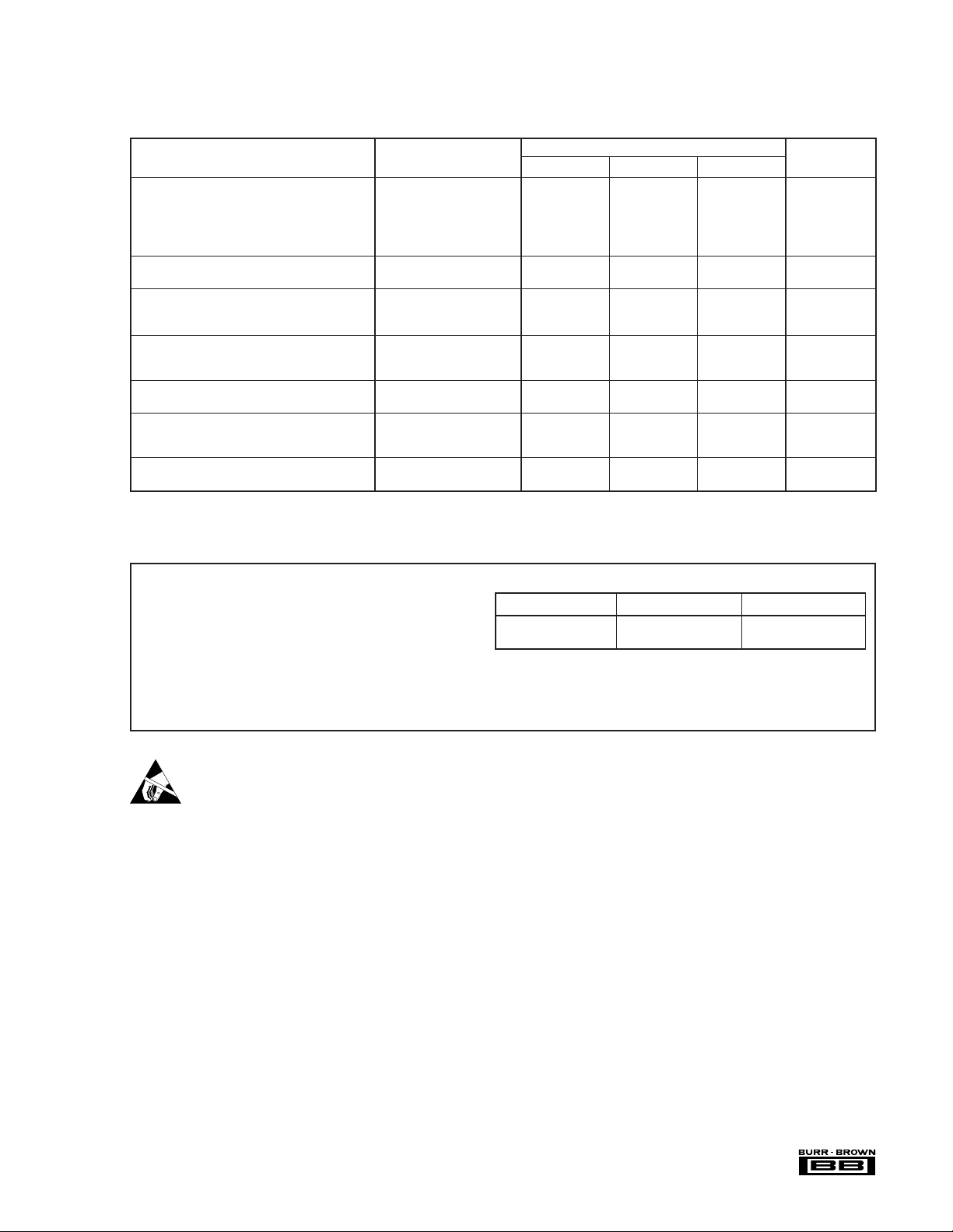
SPECIFICATIONS
At V
= ±15V and TA = +25°C, unless otherwise noted.
CC
OPA27/37G
PARAMETER CONDITIONS MIN TYP MAX UNITS
INPUT VOLTAGE
Input Offset Voltage ±48 ±220
Average Drift
Supply Rejection ±V
BIAS CURRENT
Input Bias Current ±21 ±150
OFFSET CURRENT
Input Offset Current
E, F, G 20 135
VOLTAGE RANGE
Common-Mode Input Range ±10.5
Common-Mode Rejection V
OPEN-LOOP GAIN, DC
Open-Loop Voltage Gain R
RATED OUTPUT
Voltage Output R
Short Circuit Current V
TEMPERATURE RANGE
Specification –40 +85 °C
NOTES: (1) Offset voltage specification are measured with automatic test equipment after approximately 0.5s from power turn-on. (2) Unnulled or nulled with 8kΩ to
20kΩ potentiometer. (3) This parameter guaranteed by design.
(1)
(2)
T
to T
A MIN
A MAX
= 4.5 to 18V
CC
±V
= 4.5 to 18V 90
CC
= ±11VDC 96
IN
≥ 2kΩ 113
L
= 2kΩ±11.0
L
= 0VDC 25 mA
O
(3)
(3)
(3)
(3)
(3)
±0.4 ±1.8
122 dB
±11.8 V
122 dB
120 dB
±13.4 V
(3)
(3)
(3)
(3)
µV
µV/°C
nA
nA
ABSOLUTE MAXIMUM RATINGS
Supply Voltage ................................................................................... ±22V
Internal Power Dissipation
Input Voltage ...................................................................................... ±V
Output Short-Circuit Duration
Differential Input Voltage
Differential Input Current
Storage Temperature Range ..........................................–55°C to +125°C
Operating Temperature Range.........................................–40°C to +85°C
Lead Temperature:
P (soldering, 10s) ....................................................................... +300°C
U (soldering, 3s) ......................................................................... +260°C
(1)
........................................................500mW
(2)
.................................................Indefinite
(3)
............................................................. ±0.7V
(3)
........................................................... ±25mA
CC
ELECTROSTATIC
DISCHARGE SENSITIVITY
This integrated circuit can be damaged by ESD. Burr-Brown
recommends that all integrated circuits be handled with
appropriate precautions. Failure to observe proper handling
and installation procedures can cause damage.
ESD damage can range from subtle performance degradation
to complete device failure. Precision integrated circuits may
be more susceptible to damage because very small parametric
changes could cause the device not to meet its published
specifications.
PACKAGE TYPE
8-Pin Plastic DIP (P) 100 °C/W
8-Pin SOIC (U) 160 °C/W
NOTES: (1) Maximum package power dissipation vs ambient temperature. (2) To
common with ±V
Current limiting resistors are not used in order to achieve low noise. If differential
input voltage exceeds ±0.7V, the input current should be limited to 25mA.
= 15V. (3) The inputs are protected by back-to-back diodes.
CC
θ
JA
UNITS
The information provided herein is believed to be reliable; however, BURR-BROWN assumes no responsibility for inaccuracies or omissions. BURR-BROWN assumes
no responsibility for the use of this information, and all use of such information shall be entirely at the user’s own risk. Prices and specifications are subject to change
without notice. No patent rights or licenses to any of the circuits described herein are implied or granted to any third party. BURR-BROWN does not authorize or warrant
any BURR-BROWN product for use in life support devices and/or systems.
3
OPA27, 37
®
Page 4

CONNECTION DIAGRAMS
Top View P, U Packages
Offset Trim
–V
–In
+In
1
2
3
4
CC
10Ω
8
7
6
5
0.1µF
100kΩ
DUT
Voltage Gain
Total = 50,000
Offset Trim
+V
CC
Output
NC
2kΩ
4.7µF
PACKAGE/ORDERING INFORMATION
(1)
PRODUCT
OPA27GP Plastic –40 to +85 ±100 006
OPA27GU
NOTE: (1) Packages for OPA37 are same as for OPA27. (2) OPA27GU may
be marked OPA27U. Likewise, OPA37GU may be marked OPA37U. (3) For
detailed drawing and dimension table, please see end of data sheet, or
Appendix C of Burr-Brown IC Data Book.
OPA111
100kΩ
PACKAGE RANGE (°C) MAX (µV), 25°C NUMBER
(2)
SOIC –40 to +85 ±100 182
4.3kΩ
TEMPERATURE VOLTAGE DRAWING
22µF
2.2µF
OFFSET PACKAGE
Scope
x1
= 1MΩ
R
IN
(3)
NOTE: All capacitor values are for nonpolarized capacitors only.
FIGURE 1. 0.1Hz to 10Hz Noise Test Circuit.
0.1µF
24.3kΩ
0.1Hz TO 10Hz NOISE
1s/div 40nV/div
110kΩ
FIGURE 2. Low Frequency Noise.
®
OPA27, 37
4
Page 5

TYPICAL PERFORMANCE CURVES
INPUT OFFSET VOLTAGE CHANGE
DUE TO THERMAL SHOCK
Time From Thermal Shock (min)
–1
+20
+10
0
–10
–20
Offset Voltage Change (µV)
0 +1+2+3+4+5
+25°C +70°C
T = +25°C to T = +70°C
Fluid Bath
AA
Voltage Noise (nV/√Hz)
VOLTAGE NOISE SPECTRAL DENSITY
vs TEMPERATURE
5
4
3
2
1
–75 –50 –25 0 +25 +50 +75 +100 +125
Ambient Temperature (°C)
10Hz
1kHz
At TA = +25°C, ±VCC = ±15VDC, unless otherwise noted.
+10
INPUT OFFSET VOLTAGE WARM-UP DRIFT
+5
G
0
–5
Offset Voltage Change (µV)
–10
0
123456
Time From Power Turn-On (min)
INPUT VOLTAGE NOISE vs NOISE BANDWIDTH
10
1
0.1
Voltage Noise (µVrms)
(0.1Hz to Indicated Frequency)
R = 0
S
TO-99
Ω
TOTAL INPUT VOLTAGE NOISE SPECTRAL DENSITY
100
80
60
40
20
R = 2 R
SOURCE
10
8
6
10Hz
4
Voltage Noise (nV/√Hz)
1kHz
2
vs SOURCE RESISTANCE
R
1
+
R
1
x
1
Resistor Noise Only
0.01
100 1k 10k 100k
Noise Bandwidth (Hz)
VOLTAGE NOISE SPECTRAL DENSITY
5
4
3
2
Voltage Noise (nV/√Hz)
1
0
vs SUPPLY VOLTAGE
±5 ±10 ±15 ±20
Supply Voltage (V )
1kHz
CC
10Hz
1
100 1k 10k
Source Resistance ( )Ω
®
5
OPA27, 37
Page 6

TYPICAL PERFORMANCE CURVES (CONT)
At TA = +25°C, ±VCC = ±15VDC, unless otherwise noted.
INPUT CURRENT NOISE SPECTRAL DENSITY
Current Noise (pA/√Hz)
10
0.8
0.6
0.4
0.2
8
6
4
2
1
This industry-standard equation
Warning:
is inaccurate and these figures should
Current Noise Test Circuit
10kΩ
500kΩ
100kΩ
DUT
500kΩ
√(e
I
)2 – (130nV)
=
n
n
o
1M 100
Ω x
be used for comparison purposes only!
0.1
10 100 1k 10k
Frequency (Hz)
OPEN-LOOP FREQUENCY RESPONSE
140
120
100
OPA37
80
60
Voltage Gain (dB)
40
OPA27
20
10
e
n
o
2
Voltage Noise (nV/√Hz)
INPUT VOLTAGE NOISE SPECTRAL DENSITY
8
6
4
2
0
1 10 100 1k
Frequency (Hz)
BIAS AND OFFSET CURRENT vs TEMPERATURE
20
20
Bias
15
15
Offset
10
5
Absolute Bias Current (nA)
10
5
Absolute Offset Current (nA)
0
10 100 1k 10k 100k 1M 10M 100M
Frequency (Hz)
OPA27 CLOSED-LOOP VOLTAGE GAIN AND
50
40
30
20
10
Voltage Gain (dB)
0
–10
–20
PHASE SHIFT vs FREQUENCY (G = 100)
Gain
10 100 1k 10k 100k 1M 10M 100M
Frequency (Hz)
®
OPA27, 37
0
0
–75 –50 –25 0 +25 +50 +75 +100 +125
Ambient Temperature (°C)
OPA37 CLOSED-LOOP VOLTAGE GAIN AND
50
0
–45
∅
–90
–135
–180
–225
40
30
20
10
Voltage Gain (dB)
Phase Shift (degrees)
0
–10
–20
PHASE SHIFT vs FREQUENCY (G = 100)
Ø
G = 5
Gain
10 100 1k 10k 100k 1M 10M 100M
Frequency (Hz)
0
–45
–90
–135
–180
Phase Shift (degrees)
–225
6
Page 7

TYPICAL PERFORMANCE CURVES (CONT)
OPEN-LOOP VOLTAGE GAIN vs TEMPERATURE
Voltage Gain (dB)
135
130
125
120
115
Ambient Temperature (°C)
–75 –50 –25 0 +25 +50 +75 +100 +125
RL = 2kΩ
COMMON-MODE INPUT VOLTAGE RANGE
vs SUPPLY VOLTAGE
+15
+10
+5
0
–5
–10
–15
Common-Mode Range (V)
0
Supply Voltage (V )
CC
±5 ±10 ±15 ±20
T = +25°C
A
T = +125°C
A
T = –55°C
A
T = +25°C
A
T = +125°C
A
T = –55°C
A
POWER SUPPLY REJECTION vs FREQUENCY
140
120
100
80
60
40
20
0
Power Supply Rejection (dB)
Frequency (Hz)
1 10 100 1k 10k 100k 1M 10M
OPA27
–V
CC
+V
CC
At TA = +25°C, ±VCC = ±15VDC, unless otherwise noted.
140
COMMON-MODE REJECTION vs FREQUENCY
120
100
80
60
OPA27
40
20
Common-Mode Rejection (dB)
0
1 10 100 1k 10k 100k 1M 10M
Frequency (Hz)
OPEN-LOOP VOLTAGE GAIN vs SUPPLY VOLTAGE
130
R = 2k
Ω
L
125
R = 600
Ω
L
OPA37
120
Voltage Gain (dB)
115
±5
±10 ±15 ±20 ±25
Supply Voltage (V )
SUPPLY CURRENT vs SUPPLY VOLTAGE
6
5
4
3
2
Supply Current (mA)
1
0
0
±5 ±10 ±15 ±20
Supply Voltage (V )
+125°C
+25°C
–55°C
CC
CC
®
7
OPA27, 37
Page 8

TYPICAL PERFORMANCE CURVES (CONT)
At TA = +25°C, ±VCC = ±15VDC, unless otherwise noted.
OPA27 SMALL SIGNAL TRANSIENT RESPONSE
+60
+40
+20
0
–20
Output Voltage (mV)
–40
–60
OPA27 LARGE SIGNAL TRANSIENT RESPONSE
+6
+4
+2
0
A = +1
VCL
C = 15pF
L
0
0.5 1.5 2.5
12
Time (µs)
+60
+40
+20
–20
Output Voltage (mV)
–40
–60
+15
+10
OPA37 SMALL SIGNAL TRANSIENT RESPONSE
0
0
OPA37 LARGE SIGNAL TRANSIENT RESPONSE
+5
0
0.2
A = +5
V
C = 25pF
L
0.4
0.6
Time (µs)
0.8 1.0 1.2
–2
Output Voltage (V)
–4
–6
0
2
A = +1
4
Time (µs)
VCL
81012
6
APPLICATIONS INFORMATION
OFFSET VOLTAGE ADJUSTMENT
The OPA27/37 offset voltage is laser-trimmed and will require no further trim for most applications. Offset voltage
drift will not be degraded when the input offset is nulled with
a 10kΩ trim potentiometer. Other potentiometer values from
1kΩ to 1MΩ can be used but V
an additional 0.1 to 0.2µV/°C. Nulling large system offsets
by use of the offset trim adjust will degrade drift performance
by approximately 3.3µV/°C per millivolt of offset. Large
system offsets can be nulled without drift degradation by
input summing.
The conventional offset voltage trim circuit is shown in
Figure 3. For trimming very small offsets, the higher resolution circuit shown in Figure 4 is recommended.
The OPA27/37 can replace 741-type operational amplifiers
by removing or modifying the trim circuit.
drift will be degraded by
OS
–5
Output Voltage (V)
–10
–15
1
A = +5
V
2
30456
Time (µs)
THERMOELECTRIC POTENTIALS
The OPA27/37 is laser-trimmed to microvolt-level input
offset voltage and for very low input offset voltage drift.
Careful layout and circuit design techniques are necessary to
prevent offset and drift errors from external thermoelectric
potentials. Dissimilar metal junctions can generate small
EMFs if care is not taken to eliminate either their sources
(lead-to-PC, wiring, etc.) or their temperature difference. See
Figure 11.
Short, direct mounting of the OPA27/37 with close spacing
of the input pins is highly recommended. Poor layout can
result in circuit drifts and offsets which are an order of
magnitude greater than the operational amplifier alone.
®
OPA27, 37
8
Page 9

NOISE: BIPOLAR VERSUS FET
OPA37
Output
97.6kΩ
G ≈ 40dB at 1kHz.
Metal film resistors.
Film capacitors.
R
L
and CL per cartridge
manufacturer’s
recommendations.
100Ω
2
3
6
0.03µF0.01µF
7.87kΩ
1µF
20kΩ
R
L
Moving
Magnet
Cartridge
C
L
OPA27 Output
1.9V/µs
R
F
≈ 1kΩ
Input
–
+
Low-noise circuit design requires careful analysis of all noise
sources. External noise sources can dominate in many cases,
so consider the effect of source resistance on overall operational amplifier noise performance. At low source impedances, the lower voltage noise of a bipolar operational
amplifier is superior, but at higher impedances the high
current noise of a bipolar amplifier becomes a serious liability. Above about 15kΩ the Burr-Brown OPA111 low-noise
FET operational amplifier is recommended for lower total
noise than the OPA27 (see Figure 5).
+V
CC
2
3
(1)
7
8
OPA27/37
4
±4mV Typical Trim Range
–V
CC
NOTE: (1) 10kΩ to 1MΩ
Trim Potentiometer
(10kΩ Recommended).
1
6
FIGURE 3. Offset Voltage Trim.
COMPENSATION
Although internally compensated for unity-gain stability, the
OPA27 may require a small capacitor in parallel with a
feedback resistor (R
capacitor will compensate the pole generated by R
) which is greater than 2kΩ. This
F
and C
F
and eliminate peaking or oscillation.
INPUT PROTECTION
Back-to-back diodes are used for input protection on the
OPA27/37. Exceeding a few hundred millivolts differential
input signal will cause current to flow and without external
current limiting resistors the input will be destroyed.
Accidental static discharge as well as high current can
damage the amplifier’s input circuit. Although the unit may
still be functional, important parameters such as input offset
voltage, drift, and noise may be permanently damaged as will
any precision operational amplifier subjected to this abuse.
Transient conditions can cause feedthrough due to the
amplifier’s finite slew rate. When using the OP-27 as a unitygain buffer (follower) a feedback resistor of 1kΩ is recommended (see Figure 6).
IN
+V
CC
(1)
4.7kΩ 4.7kΩ
7
8
2
OPA27/37
3
4
±280µV Typical Trim Range
–V
CC
NOTE: (1) 1kΩ Trim Potentiometer.
1
6
FIGURE 4. High Resolution Offset Voltage Trim.
1k
O
100
OPA111 + Resistor
10
Typical at 1kHz (nV/√Hz)
Voltage Noise Spectral Density, E
1
100 1k 10k 100k 1M 10M
FIGURE 5. Voltage Noise Spectral Density Versus Source
Resistance.
E
O
R
S
OPA27 + Resistor
Source Resistance, R
2
EO = √e
+ (inRS)2 + 4kTRS FO = 1kHz
n
OPA27 + Resistor
OPA111 + Resistor
Resistor Noise Only
Resistor Noise Only
(Ω)
S
FIGURE 6. Pulsed Operation.
FIGURE 7. Low-Noise RIAA Preamplifier.
1kΩ
1kΩ
Input
2
3
OPA27
FIGURE 8. Unity-Gain Inverting Amplifier.
9
OPA27, 37
6
Output
®
Page 10

Input
1kΩ
250Ω
2
3
1kΩ
OPA37
G ≈ 50dB at 1kHz.
Metal film resistors.
Film capacitors.
and CL per head
R
L
manufacturer’s
recommendations.
100Ω
6
Output
4.99kΩ
2
3
316kΩ
OPA37
0.01µF
6
1µF
Output
500pF
FIGURE 9. High Slew Rate Unity-Gain Inverting Amplifier.
Total Gain = 10
A. 741 noise with circuit well-shielded from air
currents and RFI. (Note scale change.)
B. OP-07AH with circuit well-shielded from air
currents and RFI.
6
10k
DUT
Ω
Offset
10
Ω
R
Magnetic Tape Head
C
L
L
FIGURE 10. NAB Tape Head Preamplifier.
G =1k
10Hz LowPass Filter
Chart
Recorder
10mV/mm
5mm/s
20kΩ
5µV
0.5µV
C. OPA27AJ with circuit well-shielded from air
currents and RFI. (Represents ultimate
OPA27 performance potential.)
D. OPA27 with circuit unshielded and exposed
to normal lab bench-top air currents.
(External thermoelectric potentials far
exceed OPA27 noise.)
E. OPA27 with heat sink and shield which
protects input leads from air currents.
Conditions same as (D).
FIGURE 11. Low Frequency Noise Comparison.
®
OPA27, 37
0.5µV
0.5µV
0.5µV
10
Page 11

Output
NOTE: Use metal film resistors
and plastic film capacitor. Circuit
must be well shielded to achieve
low noise.
Responsivity ≈ 2.5 x 10
4
V/W
Output Noise ≈ 30µVrms, 0.1Hz to 10Hz
Dexter 1M
Thermopile
Detector
100Ω 100kΩ
OPA27
2
3
6
0.1µF
–In
3
OPA37
2
R
F
5kΩ
R
Input Stage Gain = 1 + 2R
G
101Ω
R
5kΩ
F
Gain = 100
6
Bandwidth ≈ 500kHz
F/RG
For gain = 1000 use INA106 differential amplifier.
Burr-Brown INA105
Differential Amplifier
25kΩ 25kΩ
2
25kΩ
3
5
6
Output
+In
2
3
OPA37
6
FIGURE 12. Low Noise Instrumentation Amplifier.
1kΩ
200Ω
500pF
EDO 6166
Transducer
2
OPA37
3
1MΩ
Frequency Response
≈ 1kHz to 50kHz
6
0.1µF
FIGURE 13. Hydrophone Preamplifier.
25kΩ
1
Output
2kΩ
TTL INPUT
“1”
“0”
Input
D1
D2
TTL
In
DG188
FIGURE 15. High Performance Synchronous Demodulator.
GAIN
+1
–1
10kΩ
S1
S2
4.99kΩ
2
3
20pF
9.76kΩ
OPA27
1
Offset
Trim
4.75kΩ
1kΩ
+V
500Ω
6
8
CC
Balance
Output
4.75kΩ
Trim
FIGURE 14. Long-Wavelength Infrared Detector Amplifier.
11
OPA27, 37
®
Page 12

Input
20Ω
Gain = –1010V/V
Full Power Bandwidth ≈ 180kHz
Gain Bandwidth ≈ 500MHz
Equivalent Noise Resistance ≈ 50Ω
2
3
2kΩ
OPA37
2kΩ20Ω
6
Signal-to-Noise Ratio ∝ √N
since amplifier noise is
uncorrelated.
2kΩ
2
OPA37
3
2kΩ20Ω
2
OPA37
3
2kΩ20Ω
2
OPA37
3
2kΩ20Ω
2
OPA37
3
N = 10 Each OPA37EZ
FIGURE 16. Ultra-Low Noise “N” Stage Parallel Amplifier.
6
6
6
6
2kΩ
2kΩ
2kΩ
2kΩ
2
3
2kΩ
OPA37
6
Output
®
OPA27, 37
12
Page 13

OPA37
Output
Input
1kΩ
2
3
6
500pF
250Ω
5V
5µs
R
S
= 50Ω
+10V
0V
Output
–10V
+10V
OPA27
Output
10kΩ100Ω
100µF/20V
Tantalum
2
3
6
+
+
1
3
2
10kΩ 10kΩ
10µF/20V
Siemens LHI 948
+15V
Output
–10V
0V
R
S
= 50Ω
Input
2
3
5V
1kΩ
OPA27
5µs
6
Output
FIGURE 17. Unity-Gain Buffer.
0.01µF
VIRTEC V1000
Planar Tunnel
Diode
200ΩRFC 500pF
50Ω
Input
FIGURE 19. RF Detector and Video Amplifier.
Magnetic
FIGURE 21. Magnetic Tachometer.
2
OPA37
3
Airpax
Pickup
20kΩ200Ω
1kΩ
FIGURE 18. High Slew Rate Unity-Gain Buffer.
6
Video
Output
FIGURE 20. Balanced Pyroelectric Infrared Detector.
4.8V
2
OPA27
3
∝ RPM X N
f
OUT
Where N = Number of Gear Teeth
6
Output
13
+
0
–
®
OPA27, 37
 Loading...