

Page 1
1
®
OPA2686
OPA2686
®
Dual, Wideband, Low Noise,
Voltage Feedback OPERATIONAL AMPLIFIER
TM
©
1998 Burr-Brown Corporation PDS-1371B Printed in U.S.A. May, 2000
OPA2686 RELATED PRODUCTS
INPUT NOISE GAIN BANDWIDTH
SINGLES VOLTAGE (nV/
√Hz) PRODUCT (MHz)
OPA643 2.3 800
OPA686 1.3 1600
OPA687 0.95 3600
APPLICATIONS
● LOW NOISE, DIFFERENTIAL AMPLIFIERS
● xDSL RECEIVER AMPLIFIER
● ULTRASOUND HIGH GAIN PREAMP
● DIFFERENTIAL ADC PREAMP
● MATCHED I AND Q CHANNEL AMPLIFIERS
● MATCHED TRANSIMPEDANCE AMPLIFIERS
● PROFESSIONAL AUDIO DUAL
TRANSIMPEDANCE
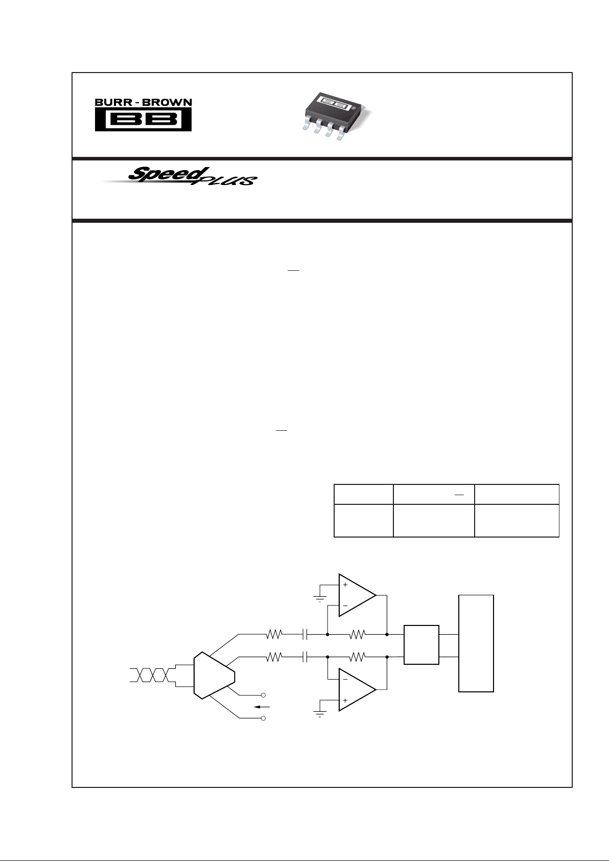
The dual channel OPA2686 provides matched channels
for high speed differencing transimpedance requirements. With over 200MHz bandwidth at a gain of
20dB, excellent gain and phase matching is provided at
IF frequencies for matched I and Q channel amplifiers.
DESCRIPTION
The OPA2686 provides two very low noise, high gain
bandwidth, voltage feedback op amps in a single
package. Operating from a low 12mA/channel quiescent current, each channel provides a 1.4nV/√Hz input
voltage noise with a 1.6GHz gain bandwidth product.
Minimum stable gain is specified at +7V/V while
exceptional flatness is guaranteed at a gain of +10.
The combination of low noise, high slew rate
(600V/µs), and broad bandwidth allow exceptional xDSL
differential receivers to be implemented. Additionally,
de-compensated, low-noise voltage-feedback op amps
are ideal for broadband transimpedance requirements.
FEATURES
● HIGH GAIN BANDWIDTH: 1.6GHz
● LOW INPUT VOLTAGE NOISE: 1.4nV/√Hz
● VERY LOW DISTORTION: –90dBc (5MHz)
● LOW SUPPLY CURRENT: 12mA/chan.
● HIGH CHANNEL ISOLATION: 70dB
● ±5V OPERATION
● STABLE FOR GAINS ≥ +7
OPA2686
1/2
OPA2686
1/2
OPA2686
R
F
R
F
R
G
R
G
Diplexer
Driver
Passive
Filter
Analog
Front
End
Low Noise VDSL Receiver
International Airport Industrial Park • Mailing Address: PO Box 11400, Tucson, AZ 85734 • Street Address: 6730 S. Tucson Blvd., Tucson, AZ 85706 • Tel: (520) 746-1111
Twx: 910-952-1111 • Internet: http://www.burr-brown.com/ • Cable: BBRCORP • Telex: 066-6491 • FAX: (520) 889-1510 • Immediate Product Info: (800) 548-6132
Page 2

2
®
OPA2686
OPA2686U
TYP GUARANTEED
0°C to –40°C to
MIN/
TEST
PARAMETER CONDITIONS +25°C +25°C
(2)
70°C
(3)
+85°C
(3)
UNITS MAX
LEVEL
(1)
SPECIFICATIONS: VS = ±5V
RF = 453Ω, RL = 100Ω, and G =+10, unless otherwise noted. Figure 1 for AC performance.
AC PERFORMANCE (Figure 1)
Closed-Loop Bandwidth G = +7, R
G
= 50Ω, VO = 200mVp-p 425 MHz typ C
G = +10, R
G
= 50Ω, VO = 200mVp-p 250 200 170 140 MHz min B
G = +20, R
G
= 50Ω, VO = 200mVp-p 100 80 65 55 MHz min B
Gain Bandwidth Product (GBP) G ≥ +40 1600 1250 1100 1000 MHz min B
Bandwidth for 0.1dB Gain Flatness G = +10, R
L
= 100Ω, VO = 200mVp-p 40 35 30 25 MHz min B
Peaking at a Gain of +7 2 dB typ C
Harmonic Distortion G = +10, f = 5MHz, V
O
= 2Vp-p
2nd Harmonic R
L
= 100Ω –72 –67 –65 –60 dBc max B
R
L
= 500Ω –90 –85 –80 –75 dBc max B
3rd Harmonic R
L
= 100Ω –95 –90 –85 –80 dBc max B
R
L
= 500Ω –110 –105 –100 –95 dBc max B
Two-Tone, 3rd-Order Intercept G = +10, f = 10MHz 43 40 39 37 dBm min B
Input Voltage Noise f > 1MHz 1.4 1.6 1.7 1.8 nV/√Hz max B
Input Current Noise f > 1MHz 1.8 2.3 2.4 2.5 pA/√Hz max B
Rise/Fall Time 0.2V Step 1.4 1.75 2 2.5 ns max B
Slew Rate 2V Step 600 500 400 310 V/µs min B
Settling Time to 0.01% 2V Step 18 ns typ C
0.1% 2V Step 16 14 21 25 ns max B
1% 2V Step 11 12 14 18 ns max B
Differential Gain G = +10, NTSC, R
L
= 150Ω 0.02 % typ C
Differential Phase G = +10, NTSC, R
L
= 150Ω 0.02 deg typ C
Channel-to-Channel Crosstalk Input Referred, f = 5MHz –70 dBc typ C
DC PERFORMANCE
(4)
Open-Loop Voltage Gain (AOL)V
O
= 0V 80 75 70 70 dB min A
Input Offset Voltage V
CM
= 0V ±0.35 ±1.0 ±1.2 ±1.5 mV max A
Average Offset Voltage Drift V
CM
= 0V 5 10 µV/°C max B
Input Bias Current V
CM
= 0V –10 –17 –18 –20 µA max A
Input Bias Current Drift V
CM
= 0V 50 100 nA/°C max B
Input Offset Current V
CM
= 0V ±0.5 ±1.0 ±1.5 ±1.8 µA max A
Input Offset Current Drift V
CM
= 0V 5 10 nA/°C max B
INPUT
Common-Mode Input Range (CMIR)
(5)
±3.2 ±3.0 ±2.9 ±2.8 V min A
Common-Mode Rejection (CMR) V
CM
= 0V, Input Referred 100 90 85 75 dB min A
Input Impedance
Differential-Mode V
CM
= 0V 6 || 2 kΩ || pF typ C
Common-Mode V
CM
= 0V 2.9 || 1 MΩ || pF typ C
OUTPUT
Output Voltage Swing ≥ 400Ω Load ±3.5
±3.2 ±3.1 ±3.0 V min A
100Ω Load ±3.3
±3.0 ±2.8 ±2.8 V min A
Current Output, Sourcing V
O
= 0V 80 60 55 50 mA min A
Current Output, Sinking V
O
= 0V –80 –60 –55 –40 mA min A
Closed-Loop Output Impedance G = +10, f = 100kHz 0.008 Ω typ C
POWER SUPPLY
Specified Operating Voltage ±5 V typ C
Maximum Operating Voltage
±6 ±6 ±6 V max A
Max Quiescent Current V
S
= ±5V 24.8 25.8 26 27.8 mA max A
Min Quiescent Current V
S
= ±5V 24.8 23.8 23.8 22 mA min A
Power Supply Rejection Ratio
+PSRR, –PSRR |V
S
| = 4.5 to 5.5, Input Referred 78 70 70 65 dB min A
THERMAL CHARACTERISTICS
Specified Operating Range: U, N Package
–40 to +85
°C typ C
Thermal Resistance,
θ
JA
Junction-to-Ambient
U SO-8 Surface Mount 125 °C/W typ C
NOTES: (1) Test Levels: (A) 100% tested at 25°C. Over temperature limits by characterization and simulation. (B) Limits set by characterization and simulation.
(C) Typical value only for information. (2) Junction temperature = ambient for 25°C guaranteed specifications. (3) Junction temperature = ambient at low temperature
limit: junction temperature = ambient +23°C at high temperature limit for over temperature guaranteed specifications. (4) Current is considered positive out-of-node.
V
CM
is the input common-mode voltage. (5) Tested < 3dB below minimum specified CMR at ±CMIR limits.
Page 3
3
®
OPA2686
The information provided herein is believed to be reliable; however, BURR-BROWN assumes no responsibility for inaccuracies or omissions. BURR-BROWN assumes
no responsibility for the use of this information, and all use of such information shall be entirely at the user’s own risk. Prices and specifications are subject to change
without notice. No patent rights or licenses to any of the circuits described herein are implied or granted to any third party. BURR-BROWN does not authorize or warrant
any BURR-BROWN product for use in life support devices and/or systems.
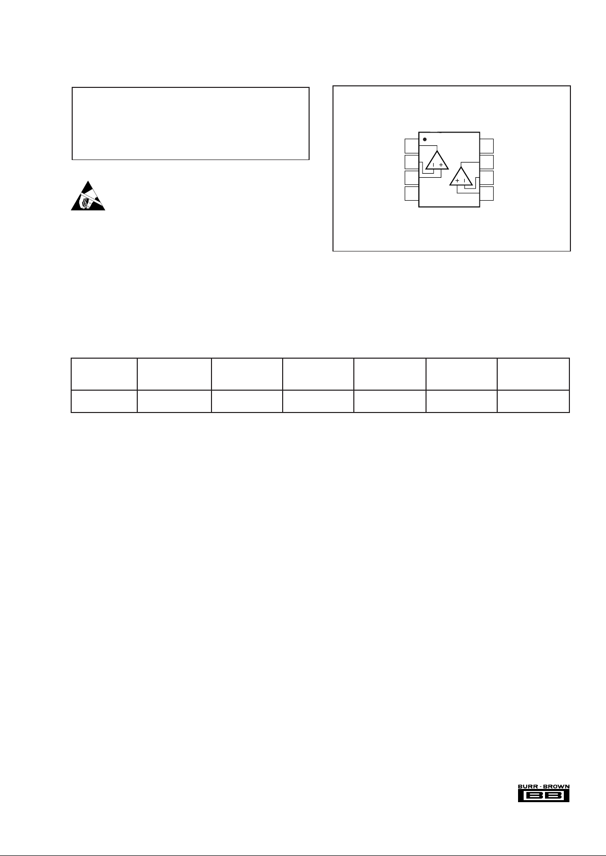
PIN CONFIGURATION
ELECTROSTATIC
DISCHARGE SENSITIVITY
This integrated circuit can be damaged by ESD. Burr-Brown
recommends that all integrated circuits be handled with appropriate
precautions. Failure to observe proper handling and installation
procedures can cause damage.
ESD damage can range from subtle performance degradation to
complete device failure. Precision integrated circuits may be more
susceptible to damage because very small parametric changes
could cause the device not to meet its published specifications.
PACKAGE
DRAWING TEMPERATURE PACKAGE ORDERING TRANSPORT
PRODUCT PACKAGE NUMBER RANGE MARKING NUMBER
(1)
MEDIA
OPA2686U SO-8 Surface Mount 182 –40°C to +85°C OPA2686U OPA2686U Rails
" """"OPA2686U/2K5 Tape and Reel
NOTES: (1) Models with a slash (/) are available only in Tape and Reel in the quantities indicated (e.g., /2K5 indicates 2500 devices per reel). Ordering 2500 pieces
of “OPA2686U/2K5” will get a single 2500-piece Tape and Reel.
PACKAGE/ORDERING INFORMATION
ABSOLUTE MAXIMUM RATINGS
Power Supply ............................................................................... ±6.5V
DC
Internal Power Dissipation ...................................... See Thermal Analysis
Differential Input Voltage .................................................................. ±1.2V
Input Voltage Range ............................................................................ ±V
S
Storage Temperature Range: U..................................... –40°C to +125°C
Lead Temperature (soldering, 10s) .............................................. +300°C
Junction Temperature (T
J
) ........................................................... +175°C
Top View SO-8
1
2
3
4
8
7
6
5
V+
Out B
–In B
+In B
Out A
–In A
+In A
V–
OPA2686
Page 4
4
®
OPA2686
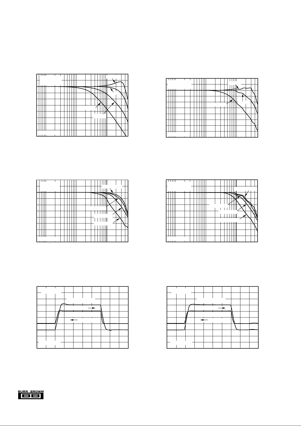
TYPICAL PERFORMANCE CURVES: VS = ±5V
At TA = +25°C, G = +10, RF = 453Ω, and RL = 100Ω, unless otherwise noted.
6
3
0
–3
–6
–9
–12
–15
–18
–21
–24
NON-INVERTING SMALL-SIGNAL
FREQUENCY RESPONSE
Frequency (MHz)
Normalized Gain (3dB/div)
0.5 10 100 500
G = +50
See Figure 1
RG = 50Ω
V
O
= 0.2Vp-p
G = +20
G = +7
G = +10
6
3
0
–3
–6
–9
–12
–15
–18
–21
–24
INVERTING SMALL-SIGNAL
FREQUENCY RESPONSE
Frequency (MHz)
Normalized Gain (3dB/div)
0.5 10 100 500
RG = RS = 50Ω
V
O
= 0.2Vp-p
G = –12
G = –50
G = –20
See Figure 2
26
23
20
17
14
11
8
5
2
–1
–4
NON-INVERTING LARGE-SIGNAL
FREQUENCY RESPONSE
Frequency (MHz)
Gain (3dB/div)
0.5 10 100 500
RG = 50Ω
G = +10V/V
VO = 0.2Vp-p
VO = 1Vp-p
VO = 2Vp-p
V
O
= 5Vp-p
See Figure 1
100
0
–100
1.5
1.0
0.5
0
–0.5
–1.0
–1.5
NON-INVERTING PULSE RESPONSE
Time (5ns/div)
Output Voltage (100mV/div)
Output Voltage (500mV/div)
G = +10V/V
Large Signal ±1V
Small Signal ±100mV
Right Scale
Left Scale
See Figure 1
100
0
–100
1.5
1.0
0.5
0
–0.5
–1.0
–1.5
INVERTING PULSE RESPONSE
Time (5ns/div)
Output Voltage (100mV/div)
Output Voltage (500mV/div)
G = –20V/V
Large Signal ±1V
Small Signal ±100mV
Right Scale
Left Scale
See Figure 2
30
29
26
23
20
17
14
11
8
5
2
INVERTING LARGE-SIGNAL
FREQUENCY RESPONSE
Frequency (MHz)
Gain (3dB/div)
0.1 10 100 500
RG = RS = 50Ω
G = –20V/V
VO = 0.2Vp-p
VO = 1Vp-p
VO = 2Vp-p
V
O
= 5Vp-p
See Figure 2
Page 5
5
®
OPA2686
TYPICAL PERFORMANCE CURVES: VS = ±5V (Cont.)
At TA = +25°C, G = +10, RF = 453Ω, and RL = 100Ω, unless otherwise noted. See Figure 1.
–60
–70
–80
–90
–100
–110
Output Voltage (Vp-p)
0.1 101
5MHz 2nd HARMONIC DISTORTION
vs OUTPUT VOLTAGE
2nd Harmonic Distortion (dBc)
RL = 100Ω
RL = 500Ω
RL = 200Ω
–60
–70
–80
–90
–100
–110
Output Voltage (Vp-p)
0.1 101
5MHz 3rd HARMONIC DISTORTION
vs OUTPUT VOLTAGE
3rd Harmonic Distortion (dBc)
RL = 500Ω
RL = 200Ω
RL = 100Ω
–55
–60
–65
–70
–75
–80
–85
–90
–95
–100
–105
Output Voltage (Vp-p)
0.1 101
10MHz 2nd HARMONIC DISTORTION
vs OUTPUT VOLTAGE
2nd Harmonic Distortion (dBc)
RL = 200Ω
RL = 100Ω
RL = 500Ω
–55
–60
–65
–70
–75
–80
–85
–90
–95
–100
–105
Output Voltage (Vp-p)
0.1 101
10MHz 3rd HARMONIC DISTORTION
vs OUTPUT VOLTAGE
3rd Harmonic Distortion (dBc)
RL = 100Ω
RL = 200Ω
RL = 500Ω
–50
–55
–60
–65
–70
–75
–80
–85
–90
–95
Output Voltage (Vp-p)
0.1 101
20MHz 2nd HARMONIC DISTORTION
vs OUTPUT VOLTAGE
2nd Harmonic Distortion (dBc)
RL = 200Ω
RL = 100Ω
RL = 500Ω
–50
–55
–60
–65
–70
–75
–80
–85
–90
–95
Output Voltage (Vp-p)
0.1 101
20MHz 3rd HARMONIC DISTORTION
vs OUTPUT VOLTAGE
3rd Harmonic Distortion (dBc)
RL = 200Ω
RL = 100Ω
RL = 500Ω
Page 6
6
®
OPA2686
TYPICAL PERFORMANCE CURVES: VS = ±5V (Cont.)
At TA = +25°C, G = +10, RF = 453Ω, and RL = 100Ω, unless otherwise noted. See Figure 1.
60
50
40
30
20
10
0
R
S
vs CAPACITIVE LOAD
Capacitive Load (pF)
1 10 100
R
S
(Ω)
22
21
20
19
18
17
16
15
14
13
12
Frequency (MHz)
FREQUENCY RESPONSE vs CAPACITIVE LOAD
1 10010 500
Gain to Capacitive Load (1dB/div)
CL = 10pF
CL = 50pF
CL = 20pF
CL = 100pF
OPA2686
R
S
V
IN
V
O
C
L
1kΩ
453Ω
50Ω
1kΩ is optional
–45
–55
–65
–75
–85
–95
–105
Frequency (MHz)
12010
2nd HARMONIC DISTORTION
vs FREQUENCY
2nd Harmonic Distortion (dBc)
VO = 2Vp-p
R
L
= 100Ω
G = +50V
G = +20
G = +10
50
45
40
35
30
25
20
15
0
TWO-TONE, 3rd-0RDER INTERMODULATION
INTERCEPT vs FREQUENCY
Frequency (MHz)
0 5 10 15 20 25 30 35 40 45 50
Intercept (dBm)
OPA2686
P
I
P
O
50Ω
50Ω
50Ω
453Ω
50Ω
–45
–55
–65
–75
–85
–95
–105
Frequency (MHz)
12010
3rd HARMONIC DISTORTION
vs FREQUENCY
3rd Harmonic Distortion (dBc)
VO = 2Vp-p
R
L
= 100Ω
G = +10
G = +50
G = +20
10
1
INPUT VOLTAGE and CURRENT NOISE DENSITY
Frequency (Hz)
100 10M1k 10k 100k 1M
Current Noise (pA/√Hz)
Voltage Noise (nV/√Hz)
1.8pA/√Hz
1.4nV/√Hz
Current Noise
Voltage Noise
Page 7

7
®
OPA2686
TYPICAL PERFORMANCE CURVES: VS = ±5V (Cont.)
At TA = +25°C, G = +10, RF = 453Ω, and RL = 100Ω, unless otherwise noted. See Figure 1.
90
80
70
60
50
40
30
20
10
0
0
–30
–60
–90
–120
–150
–180
–210
–240
–270
OPEN-LOOP GAIN and PHASE
Frequency (Hz)
100 10M 100M 1G1k 10k 100k 1M
Open-Loop Gain (10dB/div)
Open-Loop Phase (30°/div)
| AOL|
∠ A
OL
110
100
90
80
70
60
50
40
30
20
10
CMRR and PSRR
Frequency (Hz)
100 10M 100M1k 10k 100k 1M
Power Supply Rejection Ratio (dB)
CMRR
+PSRR
–PSRR
1.3
1.1
0.9
0.7
0.5
0.3
0.1
–0.1
13
11
9
7
5
3
1
–1
INPUT DC ERRORS vs TEMPERATURE
Temperature (°C)
–50 –25 0 25 50 75 100 125
V
OS
(mV)
Input Bias and Input Offset Current (µA)
Input Bias Current
Offset Voltage
Input Offset Current
10
1.0
0.1
0.01
0.001
CLOSED-LOOP OUTPUT IMPEDANCE
Frequency (Hz)
10M 100M10k 100k 1M
Output Impedance (Ω)
OPA2686
453Ω
50Ω
50Ω
Z
O
10
7
10
6
10
5
10
4
10
3
DIFFERENTIAL and COMMON-MODE
INPUT IMPEDANCE
Frequency (Hz)
100 10M 10M1k 10k 100k 1M
Input Impedance (Ω)
Common-Mode
Differential
28
24
20
16
12
8
4
0
140
120
100
80
60
40
20
0
POWER SUPPLY and OUTPUT CURRENT
vs TEMPERATURE
Temperature (°C)
–50 –25 0 25 50 75 100 125
Power Supply Current (mA)
Output Current (mA)
Power Supply Current
Output Current Sourcing
Output Current Sinking
Page 8

8
®
OPA2686
TYPICAL PERFORMANCE CURVES: VS = ±5V (Cont.)
At TA = +25°C, G = +10, RF = 453Ω, and RL = 100Ω, unless otherwise noted. See Figure 1.
–25
–35
–45
–55
–65
–75
–85
–95
–105
Frequency (MHz)
1 10010
CHANNEL-TO-CHANNEL CROSSTALK
Crosstalk (10dB/div)
Input Referred
G = +10, Both Channels
R
L
= 100Ω
Page 9

9
®
OPA2686
APPLICATIONS INFORMATION
WIDEBAND, NON-INVERTING OPERATION
The OPA2686 provides a unique combination of features—
low input voltage noise along with a very low distortion
output stage—to give one of the highest, dynamic range dual
op amps available. Its very high Gain Bandwidth Product
(GBP) can be used either to deliver high signal bandwidths
at high gains, or to deliver very low distortion signals at
moderate frequencies and lower gains. To achieve the full
performance of the OPA2686, careful attention to PC board
layout and component selection is required as discussed in
the remaining sections of this data sheet.
Figure 1 shows the non-inverting gain of +10 circuit used as
the basis of the Electrical Specifications and most of the
Typical Performance Curves. Most of the curves were characterized using signal sources with 50Ω driving impedance,
and with measurement equipment presenting a 50Ω load
impedance. In Figure 1, the 50Ω shunt resistor at the V
I
terminal matches the source impedance of the test generator,
while the 50Ω series resistor at the VO terminal provides a
matching resistor for the measurement equipment load.
Generally, data sheet voltage swing specifications are at the
output pin (VO in Figure 1), while output power (dBm)
specifications are at the matched 50Ω load. The total 100Ω
load at the output, combined with the 503Ω total feedback
network load, presents the OPA2686 with an effective output load of 83Ω for the circuit of Figure 1.
Voltage feedback op amps, unlike current feedback designs,
can use a wide range of resistor values to set their gains. The
circuit of Figure 1, and the specifications at other gains, use
the constraint that RG should always be set to 50Ω and R
F
adjusted to get the desired gain. Observing this guideline
will ensure that the thermal noise constribution of the feedback network is insignificant compared to the 1.4nV/√Hz
input voltage noise for the op amp itself.
WIDEBAND, INVERTING GAIN OPERATION
Operating the OPA2686 as an inverting amplifier has several benefits and is particularly appropriate when a matched
input impedance is required. Figure 2 shows the inverting
gain circuit used as the basis of the inverting mode Typical
Performance Curves.
FIGURE 1. Non-Inverting, G = +10 Specification and Test
Circuit.
FIGURE 2. Inverting, G = –20 Characterization Circuit.
Driving this circuit from a 50Ω source, and constraining the
gain resistor (RG) to equal 50Ω, will give both a signal
bandwidth and noise advantage. RG acts as both the input
termination resistor and the gain setting resistor for the
circuit. Although the signal gain (VO/VI) for the circuit of
Figure 2 is double that for Figure 1, the noise gains are in
fact equal when the 50Ω source resistor is included. This
has the interesting effect of doubling the equivalent GBP of
the amplifier. This can be seen in comparing the G = +10
and G = –20 small-signal frequency response curves. Both
show approximately 250MHz bandwidth, but the inverting
configuration of Figure 2 gives 6dB higher signal gain. If
the signal source is actually the low impedance output of
another amplifier, RG should be increased to the minimum
load resistance value allowed for that amplifier and R
F
should be adjusted to achieve the desired gain. For stable
operation of the OPA2686, it is critical that this driving
amplifier show a very low output impedance at frequencies
beyond the expected closed-loop bandwidth for the OPA2686.
LOW NOISE VDSL RECEIVER
Most xDSL transceiver channels are differential for both
the driver and the receiver. The low noise, high gain
bandwidth and low distortion for the dual OPA2686 make
it an ideal receiver channel element for the demanding
requirements emerging in VDSL. One possible implementation is shown on the front page of this data sheet. This
circuit is assuming full duplex communication using frequency division multiplexing with send-and-receive isola-
1/2
OPA2686
+5V
–5V
–V
S
+V
S
50Ω
V
O
V
I
50Ω
+
0.1µF
+
6.8µF
6.8µF
R
G
50Ω
R
F
453Ω
50Ω Source
50Ω Load
0.1µF
1/2
OPA2686
+5V
–5V
+V
S
–V
S
91Ω
50ΩV
O
V
I
+
6.8µF0.1µF
+
6.8µF0.1µF
0.1µF
R
F
1kΩ
R
G
50Ω
50Ω Source
50Ω Load
Page 10

10
®
OPA2686
a parasitic capacitance of 0.2pF, leaving the required 0.3pF
value shown in Figure 3 to get the required feedback pole.
This will give a –3dB bandwidth approximately equal to:
f
–3dB
= √(GBP/2πRFCD)Hz Eq. 2
The example of Figure 3 will give approximately 44MHz
flat bandwidth using the 0.3pF feedback compensation.
If the total output noise is bandlimited to a frequency less
than the feedback pole frequency, a very simple expression
for the equivalent input noise current can be derived as:
Eq. 3
Where:
IEQ= Equivalent input noise current if the output noise is
bandlimited to F < 1/(2πRFCD)
IN= Input current noise for the op amp inverting input
EN= Input voltage noise for the op amp
CD= Diode capacitance
F = Bandlimiting frequency in Hz (usually a post filter
prior to further signal processing)
Evaluating this expression up to the feedback pole frequency at 31MHz for the circuit of Figure 3 gives an
equivalent input noise current of 2.6pA/√Hz. This is only
slightly higher than the current noise of the op amp itself.
TWO-STAGE TRANSIMPEDANCE DESIGN
The dual OPA2686 may be used as either a dual
transimpedance channel from two photodectors or as a very
high gain stage by using one amplifier as the transimpedance
stage with the second used as a post gain amplifier. Figure
4 shows an example of using one channel as a transimpedance
front end from a large area detector, with the second amplifier used as a voltage gain stage to get a 100kΩ total gain
(ZT) from a large 50pF detector, (CD in Figure 4).
One key question in this design is how best to split up the
first and second stage gains. If bandwidth optimization from
a given photodetector capacitance (CD in Figure 4) is the
II
kT
R
E
R
ECF
EQ N
F
N
F
ND
=++
+
()
2
2
2
4
23π
tion improved through the use of a diplexer line interface.
The differential receive signal is brought into the inverting
channel gain resistors to get both noise and distortion
improvement for a given desired gain setting. To get
impedance matching, set 2RG equal to the required load
looking out of the diplexer. The signal gain is then set by
adjusting feedback resistors, RF. Using the OPA2686 in the
inverting mode will give you a reduced noise gain as
described in the “Wideband, Inverting Gain Operation”
section of this data sheet. This will improve both the SNR
and distortion performance. If the noise gain for a particular
application drops below the minimum recommended stable
gain (+7), consider using the Low Gain Compensation
technique described later in this data sheet.
SINGLE-STAGE TRANSIMPEDANCE DESIGN
When setting up either one or both stages as a broadband
photodiode amplifier, the key elements in the design are the
expected diode capacitance (CD) with the reverse bias voltage (–VB) applied, the desired transimpedance gain RF, and
the GBP of the OPA2686 (1600MHz). Figure 3 shows a
design using a 10pF source capacitance diode and a 10kΩ
transimpedance gain. With these three variables set (and
including the parasitic input capacitance for the OPA2686
added to CD), the feedback capacitor value (CF) may be set
to control the frequency response.
FIGURE 3. Wideband, Low Noise, Transimpedance
Amplifier.
R
F
10kΩ
Supply Decoupling
Not Shown
C
D
10pF
λ
1/2
OPA2686
+5V
–5V
–V
B
I
D
VO = ID R
F
C
F
0.3pF
FIGURE 4. High Gain, Wideband Transimpedance Amplifier.
To achieve a maximally flat 2nd-order Butterworth frequency response, the feedback pole should be set to:
1/(2πRFCF) = √(GBP/(4πRFCD)) Eq. 1
Adding the common-mode and differential mode input capacitance (1.0 + 2.0)pF to the 10pF diode source capacitance
of Figure 3, and targeting a 10kΩ transimpedance gain using
the 1600MHz GBP for the OPA2686, will require a feedback pole set to 31MHz. This will require a total feedback
capacitance of 0.5pF. Typical surface-mount resistors have
2.67kΩ
20Ω
20Ω
732Ω2.67kΩ
1/2
OPA2686
0.1µF
C
D
50pF
1.9pF
1/2
OPA2686
–V
B
λ
Page 11

11
®
OPA2686
primary goal, Equation 4 gives a solution for RF in the input
stage that will provide an equal bandwidth in the first and
second stages, giving the maximum overall channel bandwidth.
Eq. 4
Where:
ZT= Desired total transimpedance gain
CD= Diode capacitance at reverse bias
GBP = Amplifier Gain Bandwidth Product (MHz)
This equation is used to calculate the required input stage
feedback resistor in Figure 4. The remaining total signal gain
is provided by the second stage; in the example of Figure 4,
setting G = 37.5 gives the same bandwidth (approximately
42MHz) as the bandwidth achieved by the input stage. To
set this first stage bandwidth to its maximally flat values, use
Equation 5 to set the feedback capacitor value:
Eq. 5
Eq. 6
The approximate achievable bandwidth in the two stages is
given by Equation 6 which gives approximately 30MHz for
Figure 4.
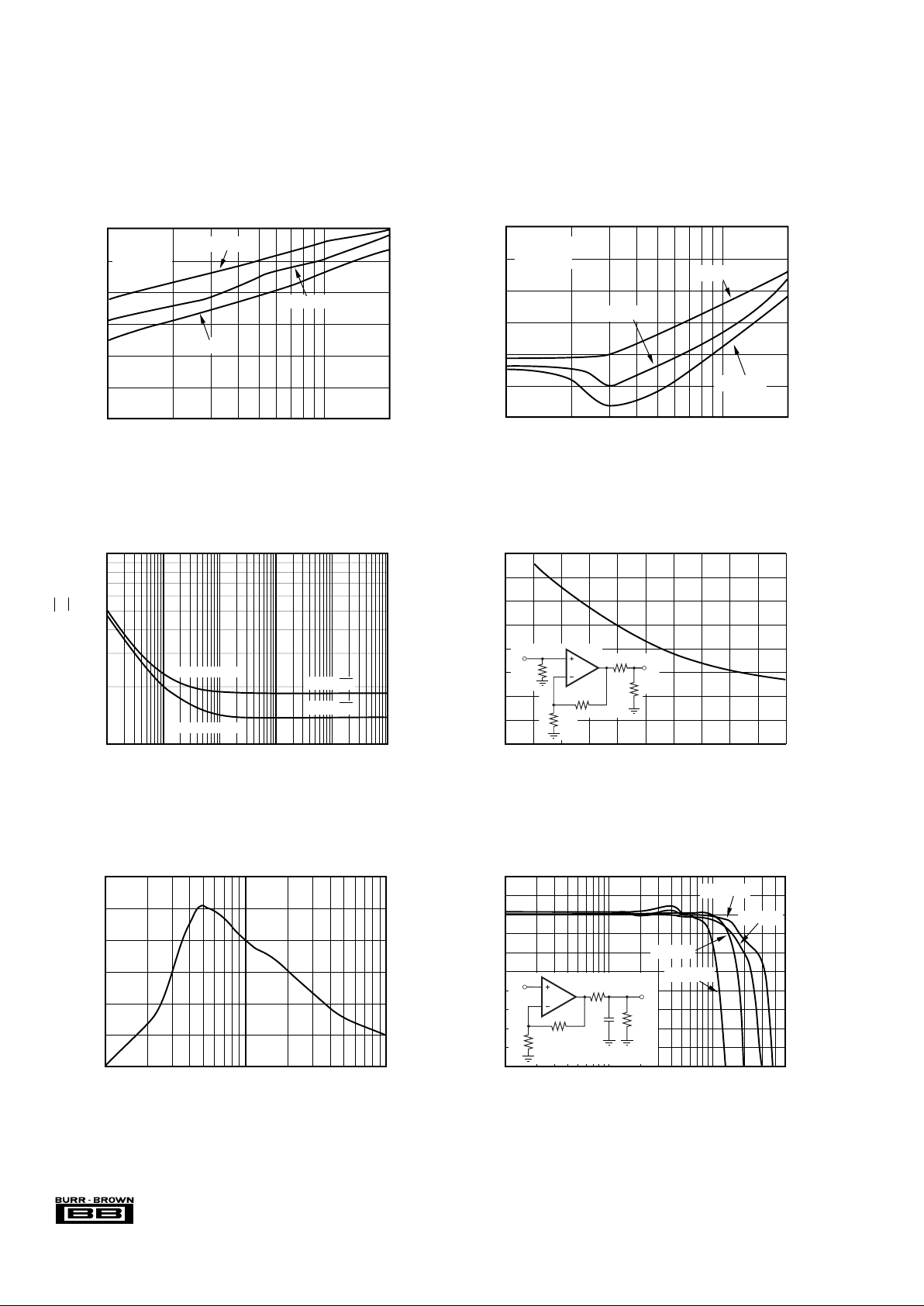
LOW GAIN COMPENSATION FOR IMPROVED SFDR
Where a low gain is desired, and inverting operation is
acceptable, a new external compensation technique may be
used to retain the full slew rate and noise benefits of the
OPA2686 while giving increased loop gain and the associated improvement in distortion offered by the decompensated architecture. This technique shapes the loop gain for
good stability while giving an easily controlled secondorder low pass frequency response. Considering only the
noise gain (non-inverting signal gain) for the circuit of
Figure 5, the low frequency noise gain, (NG1) will be set by
f
GBP
CZ
dB
DT
–
/
//
3
23
13 13
1
2
2
=
()
()()
π
R
Z
C GBP
F
T
D
=
2
13
2π
/
C
C
R GBP
F
D
F
=
π
R
F
500Ω
C
S
27pF
1/2
OPA2686
+5V
–5V
V
O
V
I
C
F
2.9pF
R
G
250Ω
FIGURE 5. Broadband Low Gain Inverting External
Compensation.
Z
GBP
NG
NG
NG
NG
NG
O
=
1
2
1
2
1
2
112–––
CF=
1
2π•R
FZO
NG
2
CS= NG2–1
()
C
F
f
–3dB
≅ ZOGBP
(= 2.86pF)
(= 27.2pF)
(= 130MHz)
the resistor ratios while the high frequency noise gain (NG2)
will be set by the capacitor ratios. The capacitor values set
both the transition frequencies and the high frequency noise
gain. If this noise gain, determined by NG2 = 1+CS/CF, is set
to a value greater than the recommended minimum stable
gain for the op amp and the noise gain pole, set by 1/RFCF,
is placed correctly, a very well controlled 2nd-order low
pass frequency response will result.
To choose the values for both CS and CF, two parameters and
only three equations need to be solved. The first parameter
is the target high frequency noise gain NG2, which should be
greater than the minimum stable gain for the OPA2686.
Here, a target NG2 of 10.5 will be used. The second parameter is the desired low frequency signal gain, which also sets
the low frequency noise gain NG1. To simplify this discussion, we will target a maximally flat second-order low pass
Butterworth frequency response (Q = 0.707). The signal
gain of –2 shown in Figure 5 will set the low frequency noise
gain to NG1 = 1 + RF/RG (NG1= 3 in this example). Then,
using only these two gains and the GBP for the OPA2686
(1600MHz), the key frequency in the compensation can be
determined as:
Eq. 7
Physically, this Z0 (10.6MHz for the values shown above) is
set by 1/(2π • RF(CF + CS)) and is the frequency at which the
rising portion of the noise gain would intersect unity gain if
projected back to 0dB gain. The actual zero in the noise gain
occurs at NG1 • Z0 and the pole in the noise gain occurs at
NG2 • Z0. Since GBP is expressed in Hz, multiply Z0 by 2π
and use this to get CF by solving:
Eq. 8
Finally, since CS and CF set the high frequency noise gain,
determine CS by:
Eq. 9
The resulting closed-loop bandwidth will be approximately
equal to:
Eq. 10
For the values shown in Figure 5, the f
–3dB
will be approximately 130MHz. This is less than that predicted by simply
dividing the GBP product by NG1. The compensation
network controls the bandwidth to a lower value while
providing the full slew rate at the output and an exceptional distortion performance due to increased loop gain at
frequencies below NG1 • Z0. The capacitor values shown
in Figure 5 are calculated for NG1 = 3 and NG2 = 10.5 with
no adjustment for parasitics.
Page 12

12
®
OPA2686
Figure 6 shows the measured frequency response for the
circuit of Figure 5. This shows the expected gain of
–2 (6dB) with exceptional flatness through 70MHz and a
–3dB bandwidth of 170MHz. Measured distortion into a
100Ω load shows > 5dB improvement through 20MHz over
the performance shown in the Typical Performance Curves.
Into a 500Ω load, the 5MHz, 2Vp-p, 2nd harmonic improves
from –85dBc to –92dBc.
DC-COUPLED, SINGLE-TO-DIFFERENTIAL ADC
DRIVER
Many very high performance CMOS ADCs are intended
to operate with a differential input signal. Translating a
single-ended source to this differential input while controlling the common-mode operating voltage can present
a considerable challenge where high SFDR is required.
Figure 7 shows one way to do this where very low
harmonic distortion is required and good common-mode
control is desired.
This particular example is set for a signal gain of 4 from
the single-ended input to the differential output voltage.
Since the common-mode control signal (from the output
of the OPA680) is fed into the midpoint of the two gain
resistors (124Ω), this DC control path requires a very low
source impedance through high frequencies to maintain
the desired signal path gain. A wideband, unity gain
stable, voltage-feedback op amp like the OPA680 makes
an ideal choice to provide this low output impedance DC
control signal. This op amp also compares the output
common-mode voltage to the desired VCM, and servos the
OPA2686 common-mode output voltage to that value
using an integrator loop. This holds the output commonmode voltage precisely at VCM while giving the low
output impedance required of the circuit.
FIGURE 6. Low Noise Figure IF Amplifier.
12
9
6
3
0
–3
–6
–9
–12
–15
–18
Frequency (MHz)
Gain (3dB/div)
1 10 100 500
170MHz
FIGURE 7. DC-Coupled, Single-to-Differential High SFDR ADC Driver.
OPA680
Power Supply De-Coupling
Not Shown
+2.5V ±2V
I
+2.5V ±2V
1/2
OPA2686
20Ω
5kΩ
130Ω
357Ω
25.5Ω
78.7Ω
+5V
20Ω
10kΩ
100Ω
10kΩ
124Ω
124Ω
357Ω
80pF
+5V
1µF
0.1µF
80pF
V–
V
CM
V+
14-Bit
10MSPS
2.2pF
+5V
–5V
1/2
OPA2686
357Ω
–5V
49.9Ω
24pF
24pF
100Ω Input
Impedance
357Ω
191Ω
2.2pF
0.1µF
+5V
V
I
Page 13

13
®
OPA2686
Each side of the OPA2686 in this circuit is operating at a
relatively low noise gain. To hold excellent frequency response flatness, the inverting gain compensation capacitors
are included at the inverting nodes and across the feedback
resistors, as described in the “Low Gain Compensation for
Improved SFDR” section in this data sheet. Operating at
+2.5V common-mode requires a DC level shifting current
through the feedback resistors. Since this current is to the
supply midpoint, pull-up resistors equal to the feedback
resistors are connected to the positive supply to keep the
output stage signal currents equal and bipolar. This significantly improves 2nd harmonic distortion.
To deliver a 2Vp-p differential input signal on a 2.5V
common-mode voltage, each output must swing between
2.0V and 3.0V. Tested harmonic distortion performance for
this condition from 1MHz to 10MHz is shown in Figure 8.
FIGURE 8. Harmonic Distortion vs Frequency for the
Circuit of Figure 7.
FIGURE 9. AC-Coupled, Single-to-Differential High SFDR ADC Driver.
–70
–75
–80
–85
–90
–95
Frequency (MHz)
110
Harmonic Distortion (dBc)
2nd Harmonic
3rd Harmonic
In this case, the 2nd harmonic distortion is still dominant
due to slight signal path imbalances—even though this
circuit does provide matched noise gain. The distortion
levels, however, are very low. Thus, narrowband applications which are impacted by only 3rd-order terms will see
very low single- and two-tone distortion levels.
AC-COUPLED, SINGLE-TO-DIFFERENTIAL ADC
DRIVER
Where the signal path may be AC-coupled, a very balanced,
high SFDR dual op amp interface circuit can easily be
provided by the OPA2686. Figure 9 shows a specific example of this application where the input single-to-differential conversion is provided by an input transformer. Once
the signal source is purely differential, the circuit of Figure
9 provides low harmonic distortion with a common-mode
control path that does not interact with the signal path gain.
If the source is already differential, such as at the output of
a balanced mixer, the input transformer could be replaced by
blocking capacitors.
In the example of Figure 9, the secondary of the transformer is connected into the two inverting path gain
resistors (100Ω). These resistors provide both an input
impedance match (assuming a 50Ω source on the primary
of this 1:2 step-up transformer) and set the signal gain for
each amplifier along with the 500Ω feedback resistors.
Although relatively high signal gain is provided by this
circuit (10 in this case), each amplifier is operating at a
relatively low noise gain (3.5 at DC). This low noise gain
at low frequencies gives high loop gain for distortion
suppression in the baseband. External compensation capacitors (18pF and 2.1pF) are included to hold the frequency response flat, as described in the “Low Gain
Single-to-Differential
Gain of 10
Power Supply De-Coupling
Not Shown
VCM +10V
I
1/2
OPA2686
20Ω
2.5V
+5V
V
CM
V
CM
20Ω
500Ω
500Ω
80pF
1µF
80pF
V–
V
CM
V+
14-Bit
10MSPS
2.1pF
1/2
OPA2686
500Ω
–5V
18pF
1000pF
1000pF
18pF
100Ω
100Ω 500Ω
2.1pF
V
I
50Ω
1:2
Page 14

14
®
OPA2686
Compensation For Improved SFDR” section of this data
sheet. The common-mode operating voltage is fed into
each amplifier’s non-inverting input. Since these are equal,
and will appear at each inverting input as well, no DC
current is produced through the transformer secondary due
to this common-mode operating voltage. Since no current
flows due to VCM, the output will operate at VCM as well.
This is one of the few common-mode operating point
control techniques that requires no current to flow. This
makes the common-mode control aspect of this circuit
essentially non-interactive with the signal path. To provide
a 2Vp-p differential signal operating at a 2.5V output
common-mode requires a 2.0V to 3.0V output swing on
each output. Tested performance over frequency for the
circuit of Figure 9 is shown in Figure 10.
centered output swing, but increases as the output is
shifted to a +2.5V DC output. Narrowband systems, where
a bandpass filter less than an octave wide can be inserted
between the amplifier and the converter, will only be
concerned about two-tone, 3rd-order intermodulation distortion. Since this bandpass filter is also AC-coupled, the
outputs of Figure 9 may be operated ground centered,
giving the extremely low 3rd-order distortions shown in
Figure 10.
DESIGN-IN TOOLS
DEMONSTRATION BOARDS
A PC board is available to assist in the initial evaluation of
circuit performance using the OPA2686. It is available free
as an unpopulated PC board delivered with descriptive
documentation. The summary information for this board is
shown in the table below.
Figure 10 shows 2nd and 3rd harmonic distortion for a
2Vp-p differential output swing at both 0V output common-mode voltage and +2.5V common-mode voltage.
Since there is no DC current required from the output to
level shift to +2.5V in this circuit, no pull-up resistors to
the power supply were used as in the circuit of Figure 7.
The 2nd harmonic remains the dominant distortion mechanism, but shows little sensitivity to the common-mode
operating voltage (improved 2nd harmonic distortion results were achieved with this circuit using two individual
OPA686N’s with an extremely symmetrical layout). The
3rd harmonic is essentially unmeasureable for the ground
FIGURE 10. Harmonic Distortion for Figure 9.
BOARD LITERATURE
PART REQUEST
PRODUCT PACKAGE NUMBER NUMBER
OPA2686U SO-8 Surface Mount DEM-OPA268xU MKT-352
Contact the Burr-Brown applications support line to request
this board.
MACROMODELS AND APPLICATIONS SUPPORT
Computer simulation of circuit performance using SPICE is
often useful when analyzing the performance of analog
circuits and systems. This is particularly true for video and
RF amplifier circuits where parasitic capacitance and inductance can have a major effect on circuit performance. A
SPICE model for the OPA2686 is available through either
the Burr-Brown Internet web page (http://www.burrbrown.com) or as one model on a disk from the Burr-Brown
Applications department (1-800-548-6132). The Applications department is also available for design assistance at this
number. These models do a good job of predicting smallsignal AC and transient performance under a wide variety of
operating conditions. They do not do as well in predicting
the harmonic distortion characteristics. These models do not
attempt to distinguish between the package types in their
small-signal AC performance.
–70
–80
–90
–100
–110
Frequency (MHz)
110
Harmonic Distortion (dBc)
VO = 2Vp-p Differential
3rd Harmonic
0V DC
+2.5V DC
0V and +2.5V DC
2nd Harmonic
Page 15

15
®
OPA2686
EE IR kT
R
NNI BS
S
=
()+()
+
22
5
4
4
3
2
4kT
R
G
R
G
R
F
R
S
1/2
OPA2686
I
BI
E
O
I
BN
4kT = 1.6E –20J
at 290°K
E
RS
E
NI
4kTRS√
4kTRF√
FIGURE 11. Op Amp Noise Analysis Model.
OPERATING SUGGESTIONS
SETTING RESISTOR VALUES TO MINIMIZE NOISE
The OPA2686 provides a very low input noise voltage while
requiring a low 12mA/channel quiescent current. To take
full advantage of this low input noise, careful attention to
the other possible noise contributors is required. Figure 11
shows the op amp noise analysis model with all the noise
terms included. In this model, all the noise terms are taken
to be noise voltage or current density terms in either nV/√Hz
or pA/√Hz.
E E I R kTR NG I R kTR NG
ONIBNS S BIF F
=+
()
+
()
+
()
+
2
2
2
2
44
E E I R kTR
IR
NG
kTR
NG
NNIBNS S
BI F F
=+
()
++
+
2
2
2
4
4
The total output spot noise voltage can be computed as the
square root of the squared contributing terms to the output
noise voltage. This computation adds all the contributing
noise powers at the output by superposition, then takes the
square root to get back to a spot noise voltage. Equation 11
shows the general form for this output noise voltage using
the terms shown in Figure 11.
Eq. 11
Dividing this expression by the noise gain (NG = 1+RF/RG)
will give the equivalent input-referred spot noise voltage at
the non-inverting input as shown in Equation 12.
Eq. 12
Inserting high resistor values into Equation 12 can quickly
dominate the total equivalent input referred noise. A 105Ω
source impedance on the non-inverting input will add a
thermal voltage noise term equal to that of the amplifier
itself. As a simplifying constraint, set RG = RS in Equation
12 and assume an RS/2 source impedance at the noninverting input (where RS is the signal’s source impedance
with another matching RS to ground on the non-inverting
input). This results in Equation 13, where NG > 10 has been
assumed to further simplify the expression.
Eq. 13
Evaluating this expression for RS = 50Ω will give a total
equivalent input noise of 1.7nV/√Hz. Note that the NG has
dropped out of this expression. This is valid only for NG
> 10.
FREQUENCY RESPONSE CONTROL
Voltage feedback op amps exhibit decreasing closed-loop
bandwidth as the signal gain is increased. In theory, this
relationship is described by the GBP shown in the specifications. Ideally, dividing GBP by the non-inverting signal
gain (also called the Noise Gain, or NG) will predict the
closed-loop bandwidth. In practice, this only holds true
when the phase margin approaches 90°, as it does in high
gain configurations. At low gains (increased feedback factor), most high speed amplifiers will exhibit a more complex
response with lower phase margin. The OPA2686 is compensated to give a maximally flat 2nd-order Butterworth
closed-loop response at a non-inverting gain of +10 (Figure
1). This results in a typical gain of +10 bandwidth of
250MHz, far exceeding that predicted by dividing the
1600MHz GBP by 10. Increasing the gain will cause the
phase margin to approach 90° and the bandwidth to more
closely approach the predicted value of (GBP/NG). At a
gain of +40, the OPA2686 will show the 40MHz bandwidth
predicted using the simple formula and the typical GBP of
1600MHz.
Inverting operation offers some interesting opportunities to
increase the available GBP. When the source impedance is
matched by the gain resistor (Figure 2), the signal gain is
(1+RF/RG) while the noise gain for bandwidth purposes is
(1 + RF/2RG). This cuts the noise gain almost in half,
increasing the minimum stable gain for inverting operation
under these condition to –12 and the equivalent GBP to
3.2GHz.
DRIVING CAPACITIVE LOADS
One of the most demanding and yet very common load
conditions for an op amp is capacitive loading. Often, the
capacitive load is the input of an A/D converter, including
additional external capacitance which may be recommended
to improve A/D linearity. A high speed, high open-loop gain
amplifier like the OPA2686 can be very susceptible to
decreased stability and closed-loop response peaking when
Page 16

16
®
OPA2686
a capacitive load is placed directly on the output pin. When
the amplifier’s open-loop output resistance is considered,
this capacitive load introduces an additional pole in the
signal path that can decrease the phase margin. Several
external solutions to this problem have been suggested.
When the primary considerations are frequency response
flatness, pulse response fidelity and/or distortion, the simplest and most effective solution is to isolate the capacitive
load from the feedback loop by inserting a series isolation
resistor between the amplifier output and the capacitive
load. This does not eliminate the pole from the loop response, but rather shifts it and adds a zero at a higher
frequency. The additional zero acts to cancel the phase lag
from the capacitive load pole, thus increasing the phase
margin and improving stability.
The Typical Performance Curves show the recommended
RS vs Capacitive Load and the resulting frequency response
at the load. Parasitic capacitive loads greater than 2pF can
begin to degrade the performance of the OPA2686. Long PC
board traces, unmatched cables, and connections to multiple
devices can easily cause this value to be exceeded. Always
consider this effect carefully, and add the recommended
series resistor as close as possible to the OPA2686 output
pin (see Board Layout Guidelines).
The criterion for setting this RS resistor is a maximum
bandwidth, flat frequency response at the load. For the
OPA2686 operating in a gain of +10, the frequency response
at the output pin is very flat to begin with, allowing relatively
small values of RS to be used for low capacitive loads. As the
signal gain is increased, the unloaded phase margin will also
increase. Driving capacitive loads at higher gains will require lower RS values than those shown for a gain of +10.
DISTORTION PERFORMANCE
The OPA2686 is capable of delivering an exceptionally low
distortion signal at high frequencies over a wide range of
gains. The distortion plots in the Typical Performance Curves
show the typical distortion under a wide variety of conditions. Most of these plots are limited to 110dB dynamic
range.
Generally, until the fundamental signal reaches very high
frequencies or powers, the 2nd harmonic will dominate the
distortion with negligible a 3rd harmonic component. Focusing then on the 2nd harmonic, increasing the load impedance
improves distortion directly. Remember that the total load
includes the feedback network; in the non-inverting configuration, this is sum of RF + RG, while in the inverting
configuration, it is just RF (Figures 1 and 2). Increasing
output voltage swing increases harmonic distortion directly.
A 6dB increase in output swing will generally increase the
2nd harmonic 12dB and the 3rd harmonic 18dB. Increasing
the signal gain will also increase the 2nd harmonic distortion. Again, a 6dB increase in gain will increase the 2nd and
3rd harmonic by approximately 6dB even with constant
output power and frequency. Finally, the distortion increases
as the fundamental frequency increases due to the rolloff in
the loop gain with frequency. Conversely, the distortion will
improve going to lower frequencies down to the dominant
open-loop pole at approximately 100kHz. Starting from the
–82dBc 2nd harmonic for a 5MHz, 2Vp-p fundamental into
a 200Ω load at G = +10 (from the Typical Performance
Curves), the 2nd harmonic distortion for frequencies lower
than 100kHz will be approximately –82dBc – 20log(5MHz/
100kHz) = –116dBc.
The OPA2686 has extremely low 3rd-order harmonic distortion. This also gives a high two-tone, 3rd-order
intermodulation intercept as shown in the Typical Performance Curves. This intercept curve is defined at the 50Ω
load when driven through a 50Ω matching resistor to allow
direct comparisons to RF MMIC devices. This matching
network attenuates the voltage swing from the output pin to
the load by 6dB. If the OPA2686 drives directly into the
input of a high impedance device, such as an ADC, the 6dB
attenuation is not taken. Under these conditions, the intercept will increase by a minimum 6dBm. The intercept is
used to predict the intermodulation spurious for two, closelyspaced frequencies. If the two test frequencies, f1 and f2, are
specified in terms of average and delta frequency, fO =
(f1 + f2)/2 and ∆f = |f2 – f1|/2, the two 3rd-order, close-in
spurious tones will appear at fO ±3 • ∆f. The difference
between two equal test-tone power levels and these
intermodulation spurious power levels is given by
∆dBc = 2 • (IM3 – PO) where IM3 is the intercept taken
from the Typical Performance Curve and PO is the power
level in dBm at the 50Ω load for one of the two closelyspaced test frequencies. For instance, at 5MHz the OPA2686
at a gain of +10 has an intercept of 48dBm at a matched 50Ω
load. If the full envelope of the two frequencies needs to be
2Vp-p, this requires each tone to be 4dBm. The 3rd-order
intermodulation spurious tones will then be 2 • (48 – 4) =
88dBc below the test-tone power level (–84dBm). If this
same 2Vp-p, two-tone envelope were delivered directly into
the input of an ADC—without the matching loss or the
loading of the 50Ω network—the intercept would increase
to at least 54dBm. With the same signal and gain conditions, but now driving directly into a light load, the spurious
tones will then be at least 2 • (54 – 4) = 100dBc below the
4dBm test-tone power levels centered on 5MHz.
DC ACCURACY AND OFFSET CONTROL
The OPA2686 can provide excellent DC signal accuracy
due to its high open-loop gain, high common-mode rejection, high power supply rejection, and low input offset
voltage and bias current offset errors. To take full advantage
of its low ±1.5mV input offset voltage, careful attention to
input bias current cancellation is also required. The low
noise input stage of the OPA2686 has a relatively high input
bias current (10µA typical into the pins) but with a very
close match between the two input currents—typically
±100nA input offset current. The total output offset voltage
may be reduced considerably by matching the source impedances looking out of the two inputs. For example, one
way to add bias current cancellation to the circuit of Figure
1 would be to insert a 20Ω series resistor into the noninverting input from the 50Ω terminating resistor. When the
Page 17

17
®
OPA2686
FIGURE 12. DC-Coupled, Inverting Gain of –20, with
Output Offset Adjustment.
50Ω source resistor is DC-coupled, this will increase the
source resistances for the non-inverting input bias current to
45Ω. Since this is now equal to the resistance looking out of
the inverting input (RF || RG), the circuit will cancel the gains
for the bias currents to the output leaving only the offset
current times the feedback resistor as a residual DC error
term at the output. Using the 453Ω feedback resistor, this
output error will now be less than ±0.9µA • 453Ω = ±0.4mV
over the full temperature range.
A fine-scale output offset null, or DC operating point adjustment, is often required. Numerous techniques are available
for introducing a DC offset control into an op amp circuit.
Most of these techniques eventually reduce to setting up a
DC current through the feedback resistor. One key consideration to selecting a technique is to insure that it has a
minimal impact on the desired signal path frequency response. If the signal path is intended to be non-inverting, the
offset control is best applied as an inverting summing signal
to avoid interaction with the signal source. If the signal path
is intended to be inverting, applying the offset control to the
non-inverting input can be considered. For a DC-coupled
inverting input signal, this DC offset signal will set up a DC
current back into the source that must be considered. An
offset adjustment placed on the inverting op amp input can
also change the noise gain and frequency response flatness.
Figure 12 shows one example of an offset adjustment for a
DC-coupled signal path that will have minimum impact on
the signal frequency response. In this case, the input is
brought into an inverting gain resistor with the DC adjustment an additional current summed into the inverting node.
The resistor values setting this offset adjustment are much
larger than the signal path resistors. This will insure that this
adjustment has minimal impact on the loop gain and hence,
the frequency response.
THERMAL ANALYSIS
The OPA2686 will not require heatsinking or airflow in
most applications. Maximum desired junction temperature
will set the maximum allowed internal power dissipation as
described below. In no case should the maximum junction
temperature be allowed to exceed +175°C.
Operating junction temperature (TJ) is given by TA + PD •
θ
JA
. The total internal power dissipation (PD) is the sum of
quiescent power (PDQ) and additional power dissipated in
the output stage (PDL) to deliver load power. Quiescent
power is simply the specified no-load supply current times
the total supply voltage across the part. PDL will depend on
the required output signal and load but would, for a grounded
resistive load, be at a maximum when the output is fixed at
a voltage equal to 1/2 either supply voltage (for equal bipolar
supplies). Under this worst-case condition, PDL = V
S
2
/(4 •
RL) where RL includes feedback network loading.
Note that it is the power in the output stage and not in the
load that determines internal power dissipation.
As a worst-case example, compute the maximum TJ using
both channels of the OPA2686U in the circuit of Figure 1
operating at the maximum specified ambient temperature of
+85°C and driving a grounded 100Ω load at +2.5VDC:
PD = 10V • (27.8mA) + 2 • [52/(4 • (100Ω || 500Ω))] = 428mW
Maximum TJ = +85°C + (0.428W • 125°C/W) = 139°C
This absolute worst-case example will never be encountered
in practice. Therefore, 139°C sets an upper limit to maximum junction temperature.
BOARD LAYOUT
Achieving optimum performance with a high frequency
amplifier like the OPA2686 requires careful attention to
board layout parasitics and external component types. Recommendations that will optimize performance include:
a) Minimize parasitic capacitance to any AC ground for
all of the signal I/O pins. Parasitic capacitance on the
output and inverting input pins can cause instability: on the
non-inverting input, it can react with the source impedance
to cause unintentional bandlimiting. To reduce unwanted
capacitance, a window around the signal I/O pins should be
opened in all of the ground and power planes around those
pins. Otherwise, ground and power planes should be unbroken elsewhere on the board.
b) Minimize the distance (< 0.25") from the power
supply pins to high frequency 0.1µF decoupling capacitors. At the device pins, the ground and power plane layout
should not be in close proximity to the signal I/O pins. Avoid
narrow power and ground traces to minimize inductance
between the pins and the decoupling capacitors. The power
supply connections should always be decoupled with these
capacitors. Larger (2.2µF to 6.8µF) decoupling capacitors,
effective at lower frequency, should also be used on the
main supply pins. These may be placed somewhat farther
from the device and may be shared among several devices in
the same area of the PC board.
R
F
1kΩ
±200mV Output Adjustment
= – = –20
Supply Decoupling
Not Shown
5kΩ
5kΩ
48Ω
0.1µF
R
G
50Ω
V
I
20kΩ
10kΩ
0.1µF
–5V
+5V
1/2
OPA2686
+5V
–5V
V
O
V
O
V
I
R
F
R
G
Page 18

18
®
OPA2686
External
Pin
+V
CC
–V
CC
Internal
Circuitry
FIGURE 13. Internal ESD Protection.
c) Careful selection and placement of external components will preserve the high frequency performance of
the OPA2686. Resistors should be a very low reactance
type. Surface-mount resistors work best and allow a tighter
overall layout. Metal-film and carbon composition, axiallyleaded resistors can also provide good high frequency performance. Again, keep their leads and PC board trace length
as short as possible. Never use wirewound type resistors in
a high frequency application. Since the output pin and
inverting input pin are the most sensitive to parasitic capacitance, always position the feedback and series output resistor, if any, as close as possible to the output pin. Other
network components, such as non-inverting input termination resistors, should also be placed close to the package.
Where double-side component mounting is allowed, place
the feedback resistor directly under the package on the other
side of the board between the output and inverting input
pins. Even with a low parasitic capacitance shunting the
external resistors, excessively high resistor values can create
significant time constants that can degrade performance.
Good axial metal-film or surface-mount resistors have approximately 0.2pF in shunt with the resistor. For resistor
values > 1.5kΩ, this parasitic capacitance can add a pole
and/or a zero below 500MHz that can effect circuit operation. Keep resistor values as low as possible consistent with
load driving considerations. It has been suggested here that
a good starting point for design would be to set RG to 50Ω.
Doing this will automatically keep the resistor noise terms
low, and minimize the effect of their parasitic capacitance.
d) Connections to other wideband devices on the board
may be made with short direct traces or through onboard transmission lines. For short connections, consider
the trace and the input to the next device as a lumped
capacitive load. Relatively wide traces (50mils to 100mils)
should be used, preferably with ground and power planes
opened up around them. Estimate the total capacitive load
and set RS from the plot of recommended RS vs Capacitive
Load. Low parasitic capacitive loads (< 5pF) may not need
an RS since the OPA2686 is nominally compensated to
operate with a 2pF parasitic load. Higher parasitic capacitive
loads without an RS are allowed as the signal gain increases
(increasing the unloaded phase margin). If a long trace is
required, and the 6dB signal loss intrinsic to a doublyterminated transmission line is acceptable, implement a
matched impedance transmission line using microstrip or
stripline techniques (consult an ECL design handbook for
microstrip and stripline layout techniques). A 50Ω environment is normally not necessary on board, and in fact, a
higher impedance environment will improve distortion as
shown in the distortion versus load plots. With a characteristic board trace impedance defined based on board material
and trace dimensions, a matching series resistor into the
trace from the output of the OPA2686 is used as well as a
terminating shunt resistor at the input of the destination
device. Remember also that the terminating impedance will
be the parallel combination of the shunt resistor and the
input impedance of the destination device; this total effective impedance should be set to match the trace impedance.
If the 6dB attenuation of a doubly-terminated transmission
line is unacceptable, a long trace can be series-terminated at
the source end only. Treat the trace as a capacitive load in
this case and set the series resistor value as shown in the plot
of RS vs Capacitive Load. This will not preserve signal
integrity as well as a doubly-terminated line. If the input
impedance of the destination device is low, there will be
some signal attenuation due to the voltage divider formed by
the series output into the terminating impedance.
e) Socketing a high speed part like the OPA2686 is not
recommended. The additional lead length and pin-to-pin
capacitance introduced by the socket can create an extremely troublesome parasitic network which can make it
almost impossible to achieve a smooth, stable frequency
response. Best results are obtained by soldering the OPA2686
onto the board.
INPUT AND ESD PROTECTION
The OPA2686 is built using a very high speed complementary bipolar process. The internal junction breakdown voltages are relatively low for these very small geometry devices. These breakdowns are reflected in the Absolute Maximum Ratings table. All device pins are protected with
internal ESD protection diodes to the power supplies as
shown in Figure 13.
These diodes provide moderate protection to input overdrive
voltages above the supplies as well. The protection diodes
can typically support 30mA continuous current. Where higher
currents are possible (e.g., in systems with ±15V supply
parts driving into the OPA2686), current-limiting series
resistors should be added into the two inputs. Keep these
resistor values as low as possible since high values degrade
both noise performance and frequency response.
 Loading...