

Page 1
SBOS286A − DECEMBER 2003 − REVISED SEPTEMBER 2006
Please be aware that an important notice concerning availability, standard warranty, and use in critical applications of Texas Instruments
High-Performance, Fully-Differential
AUDIO OP AMP
OPA1632
FEATURES
D SUPERIOR SOUND QUALITY
D ULTRA LOW DISTORTION: 0.000022%
D LOW NOISE: 1.3nV/√Hz
D HIGH SPEED:
− Slew Rate: 50V/µs
− Gain Bandwidth: 180MHz
D FULLY DIFFERENTIAL ARCHITECTURE:
− Balanced Input and Output Converts
Single-Ended Input to Balanced
Differential Output
D WIDE SUPPLY RANGE: ±2.5V to ±16V
D SHUTDOWN TO CONSERVE POWER
APPLICATIONS
D AUDIO ADC DRIVER
D BALANCED LINE DRIVER
D BALANCED RECEIVER
D ACTIVE FILTER
D PREAMPLIFIER
DESCRIPTION
The OPA1632 is a fully-differential amplifier designed
for driving high-performance audio analog-to-digital
converters (ADCs). It provides the highest audio quality ,
with very low noise and output drive characteristics
optimized for this application. The OPA1632’s excellent
gain bandwidth of 180MHz and very fast slew rate of
50V/µs produce exceptionally low distortion. Very low
input noise of 1.3nV/√Hz further ensures maximum
signal-to-noise ratio and dynamic range.
The flexibility of the fully differential architecture allows
for easy implementation of a single-ended to
fully-differential output conversion. Differential output
reduces even-order harmonics and minimizes
common-mode noise interference. The OPA1632
provides excellent performance when used to drive
high-performance audio ADCs such as the PCM1804.
A shutdown feature also enhances the flexibility of this
amplifier.
The OPA1632 is available in an SO-8 package and a
thermally-enhanced MSOP-8 PowerPAD package.
RELATED DEVICES
OPAx134 High-Performance Audio Amplifiers
OPA627/637 Precision High-Speed DiFET Amplifiers
OPAx227/x228 Low-Noise Bipolar Amplifiers
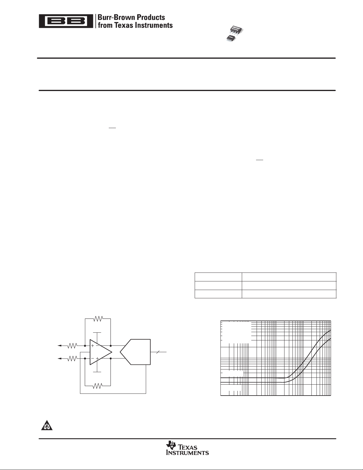
0.001
+15V
V
IN+
V
V
IN−
semiconductor products and disclaimers thereto appears at the end of this data sheet.
PowerPAD is a trademark of Texas Instruments. All other trademarks are the property of their respective owners.
! !
OCM
−
15V
Typical ADC Circuit
−
V
IN
V
+
IN
Digital
Output
V
COM
www.ti.com
0.0001
THD + Noise (%)
0.00001
Gain = +1
R
F
V
O
Differential I/O
RL=600
RL=2k
THD + NOISE vs FREQUENCY
Ω
= 348
=3Vrms
Ω
Ω
100010 100 10k 100k
Frequency (Hz)
Copyright 2003−2006, Texas Instruments Incorporated
Page 2
"#$%
SO-8
D
−40°C to +85°C
OPA1632
OPA1632
MSOP-8
MSOP-8
DGN
−40°C to +85°C
1632
SBOS286A − DECEMBER 2003 − REVISED SEPTEMBER 2006
www.ti.com
PACKAGE/ORDERING INFORMATION
(1)
SPECIFIED
PRODUCT PACKAGE-LEAD
PACKAGE
DRAWING
TEMPERATURE
RANGE
PACKAGE
MARKING
ORDERING
NUMBER
TRANSPORT
MEDIA, QUANTITY
OPA1632D Rails, 100
OPA1632DR Tape and Reel, 2500
OPA1632DGN Rails, 100
PowerPAD
(1)
For the most current package and ordering information see the Package Option Addendum at the end of this document, or see the TI web site
OPA1632DGNR Tape and Reel, 2500
at www .ti.com.
ABSOLUTE MAXIMUM RATINGS
over operating free-air temperature range unless otherwise noted.
Supply Voltage, ±V
Input Voltage, V
Output Current, I
Differential Input Voltage, V
Maximum Junction Temperature, T
Operating Free-Air Temperature Range −40°C to +85°C. . . . . . . . . . . . . . .
Storage Temperature Range, T
ESD Ratings: Human Body Model 1kV. . . . . . . . . . . . . . . . . . . . . . . . . . . . . .
(1)
Stresses above these ratings may cause permanent damage.
S
. . . . . . . . . . . . . . . . . . . . . . . . . . . . . . . . . . . . . . . . . . . . .
I
O
Charge Device Model 500V. . . . . . . . . . . . . . . . . . . . . . . . . . .
Machine Model 200V. . . . . . . . . . . . . . . . . . . . . . . . . . . . . . . . .
ID
J
STG
(1)(2)
−65°C to +150°C. . . . . . . . . . . . . . . . .
±16.5V. . . . . . . . . . . . . . . . . . . . . . . . . . . . . . . . . . . . . . .
±V
S
150mA. . . . . . . . . . . . . . . . . . . . . . . . . . . . . . . . . . . . . . . .
±3V. . . . . . . . . . . . . . . . . . . . . . . . . . . . . . . . . .
150°C. . . . . . . . . . . . . . . . . . . . . . . . . .
proper handling and installation procedures can cause damage.
ESD damage can range from subtle performance degradation to
complete device failure. Precision integrated circuits may be more
susceptible t o damage because very small parametric changes could
cause the device not to meet its published specifications.
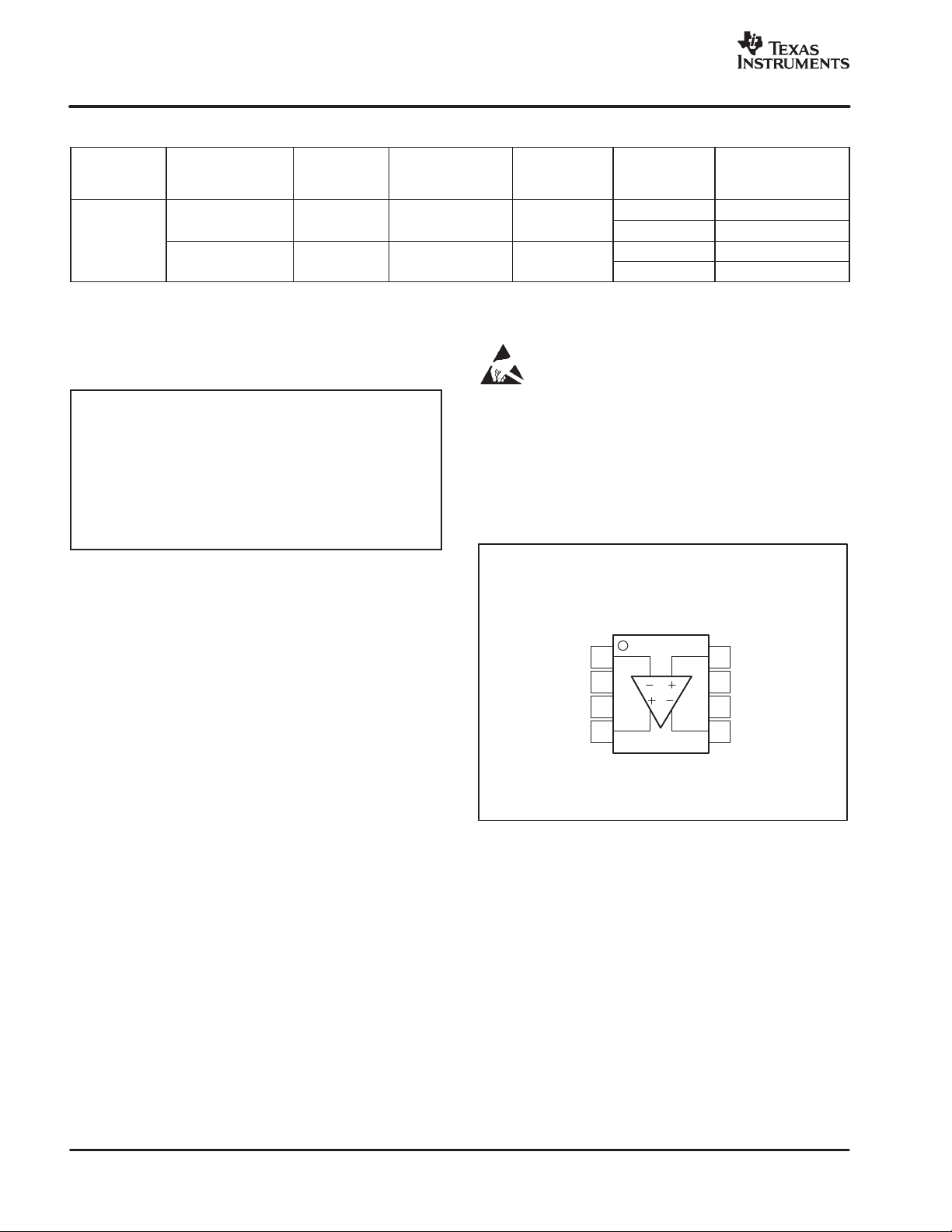
PIN CONFIGURATION
Top View MSOP, SO
This integrated circuit can be damaged by ESD. Texas
Instruments recommends that all integrated circuits be
handled with appropriate precautions. Failure to observe
Exposure to absolute maximum conditions for extended periods
may degrade device reliability. These are stress ratings only , an d
functional operation of the device at these or any other conditions
beyond those specified is not implied.
(2)
The OPA1632 MSOP-8 package version incorporates a
PowerPAD on the underside of the chip. This acts as a heatsink
and must be connected to a thermally dissipative plane for proper
power dissipation. Failure to do so may result in exceeding the
maximum junction temperature, which can permanently damage
the device. See TI technical brief SLMA002 for more information
about using the PowerPAD thermally enhanced package.
V
V
V
OCM
V+
OUT+
−
IN
OPA1632
1
2
3
4
V
8
IN+
Enable
7
−
V
6
V
5
OUT−
2
Page 3
"#$%
www.ti.com
SBOS286A − DECEMBER 2003 − REVISED SEPTEMBER 2006
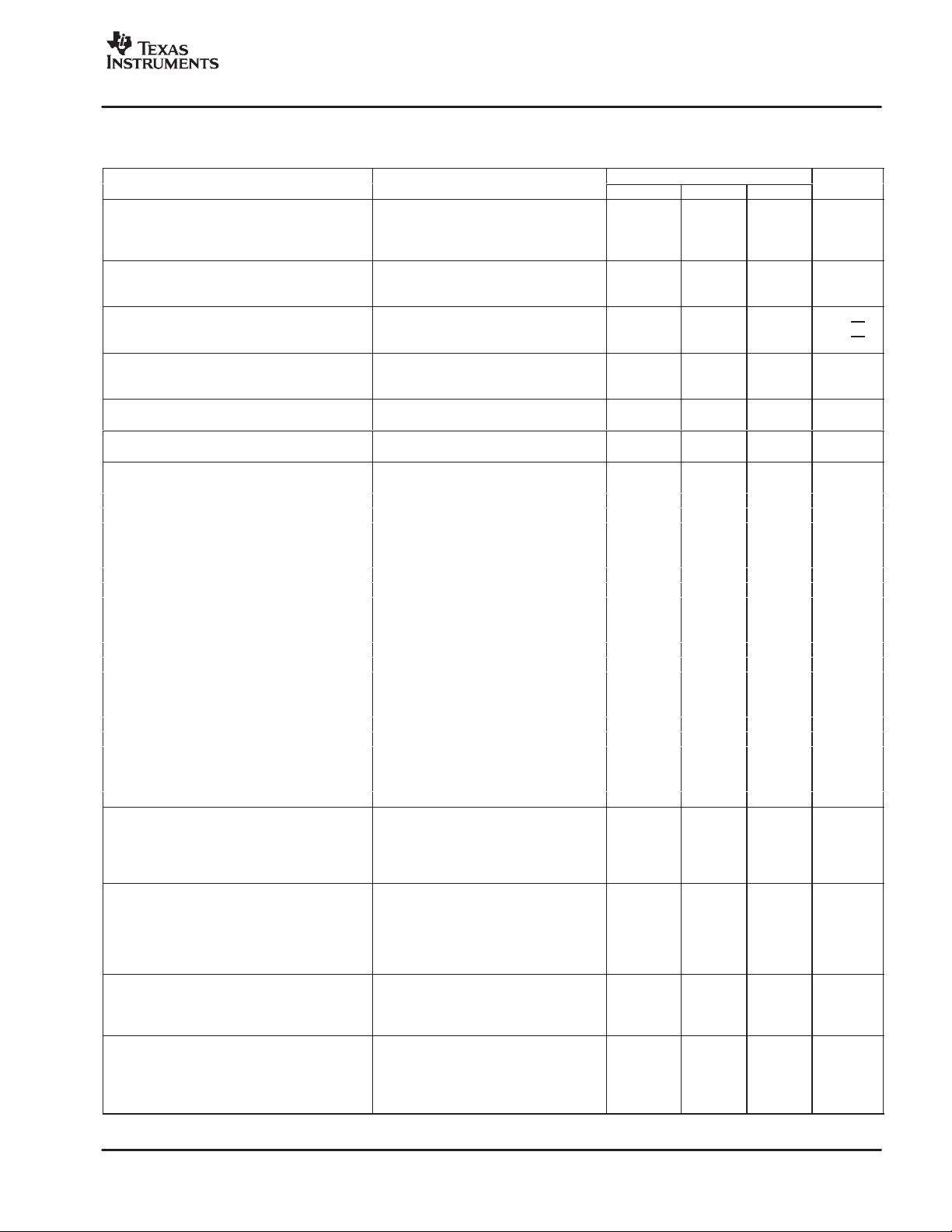
ELECTRICAL CHARACTERISTICS: VS = ±15V
VS = ±15V: RF = 390Ω, RL = 800Ω, and G = +1, unless otherwise noted.
PARAMETER CONDITIONS MIN TYP MAX UNITS
OFFSET VOLTAGE
Input Offset Voltage ±0.5 ±3 mV
vs Temperature dVos/dT ±5 µV/_C
vs Power Supply, DC PSRR 316 13 µV/V
INPUT BIAS CURRENT
Input Bias Current I
Input Offset Current I
NOISE
Input Voltage Noise f = 10 kHz 1.3 nV/√Hz
Input Current Noise f = 10 kHz 0.4 pA/√Hz
INPUT VOLTAGE
Common-Mode Input Range (V−) + 1.5 (V+) − 1 V
Common-Mode Rejection Ratio, DC 74 90 dB
INPUT IMPEDANCE
Input Impedance (each input pin) 34 || 4 MΩ || pF
OPEN-LOOP GAIN
Open-Loop Gain , DC 66 78 dB
FREQUENCY RESPONSE
Small-Signal Bandwidth G = +1, RF= 348Ω 180 MHz
(VO = 100mVPP, Peaking < 0.5 dB) G = +2, RF = 602Ω 90 MHz
Bandwidth for 0.1dB Flatness G = +1, VO = 100mV
Peaking at a Gain of 1 VO = 100mV
Large-Signal Bandwidth G = +2, VO = 20V
Slew Rate (25% to 75% ) G = +1 50 V/µs
Rise and Fall Time G = +1, VO = 5V Step 100 ns
Settling Time to 0.1% G = +1, VO = 2V Step 75 ns
0.01% G = +1, VO = 2V Step 200 ns
Total Harmonic Distortion + Noise G = +1, f = 1kHz, VO = 3Vrms
Differential Input/Output RL = 600Ω 0.0003 %
Differential Input/Output RL = 2kΩ 0.000022 %
Single-Ended In/Differential Out RL = 600Ω 0.000059 %
Single-Ended In/Differential Out RL = 2kΩ 0.000043 %
Intermodulation Distortion G = +1, SMPTE/DIN, VO = 2V
Differential Input/Output RL = 600Ω 0.00008 %
Differential Input/Output RL = 2kΩ 0.00005 %
Single-Ended In/Differential Out RL = 600Ω 0.0001 %
Single-Ended In/Differential Out RL = 2kΩ 0.0007 %
Headroom THD < 0.01%, RL = 2kΩ 20.0 V
OUTPUT
Voltage Output Swing RL = 2kΩ (V+) − 1.9 (V−) + 1.9 V
Short-Circuit Current I
Closed-Loop Output Impedance G = +1, f = 100kHz 0.3 Ω
POWER-DOWN
Enable Voltage Threshold (V−) + 2 V
Disable Voltage Threshold (V−) + 0.8 V
Shutdown Current V
Turn-On Delay Time for IQ to Reach 50% 2 µs
Turn-Off Delay Time for IQ to Reach 50% 2 µs
POWER SUPPL Y
Specified Operating Voltage ±15 ±16 V
Operating Voltage ±2.5 V
Quiescent Current I
TEMPERATURE RANGE
Specified Range −40 +85 _C
Operating Range −40 +125 _C
Storage Range −65 +150 _C
Thermal Resistance
(1)
Amplifier has internal 50kΩ pull-up resistor to V
(1)
OS
SC
B
G = +5, RF = 1.5kΩ 36 MHz
G = +10, RF = 3.01kΩ 18 MHz
PP
PP
PP
PP
RL = 800Ω (V+) − 4.5 (V−) + 4.5 V
Sourcing/Sinking +50/−60 85 mA
= −15V 0.85 1.5 mA
ENABLE
Q
q
JA
pin. This enables the amplifier with no connection to shutdown pin.
CC+
Per Channel 14 17.1 mA
OPA1632
2 6 µA
±100 ±500 nA
40 MHz
0.5 dB
800 kHz
PP
200 _C/W
3
Page 4
"#$%
SBOS286A − DECEMBER 2003 − REVISED SEPTEMBER 2006
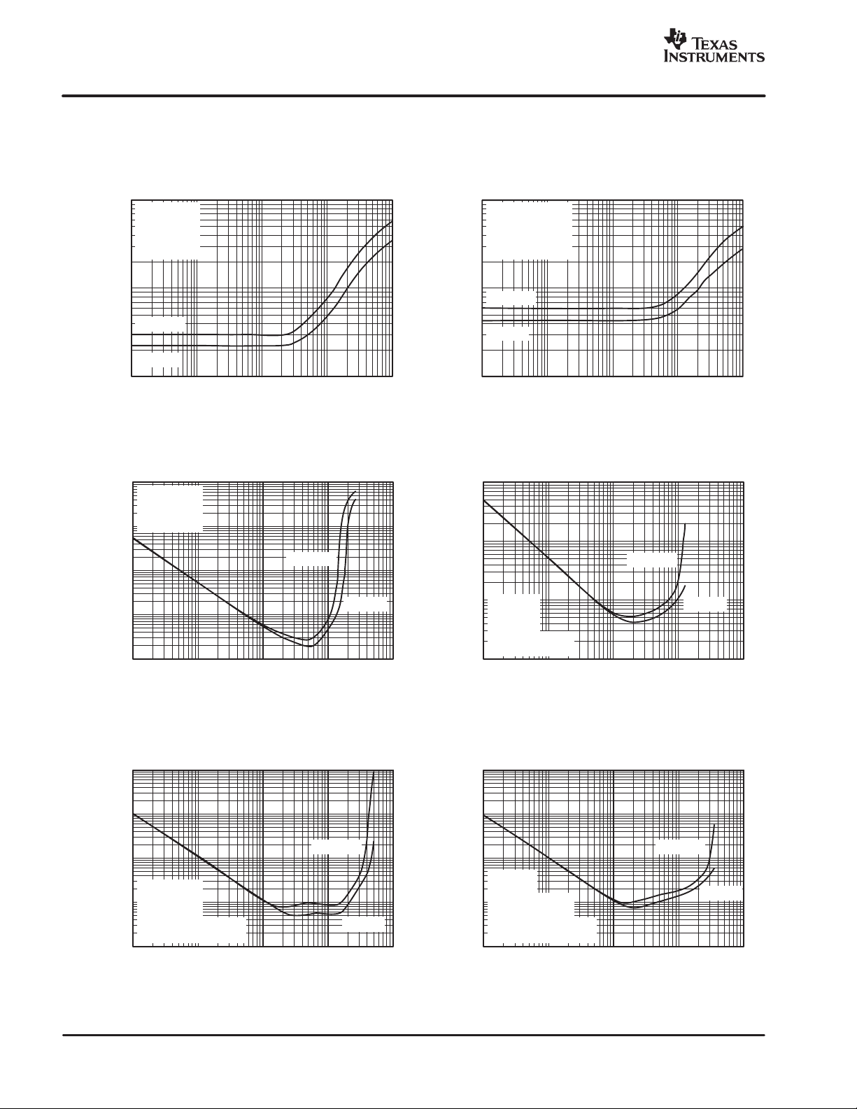
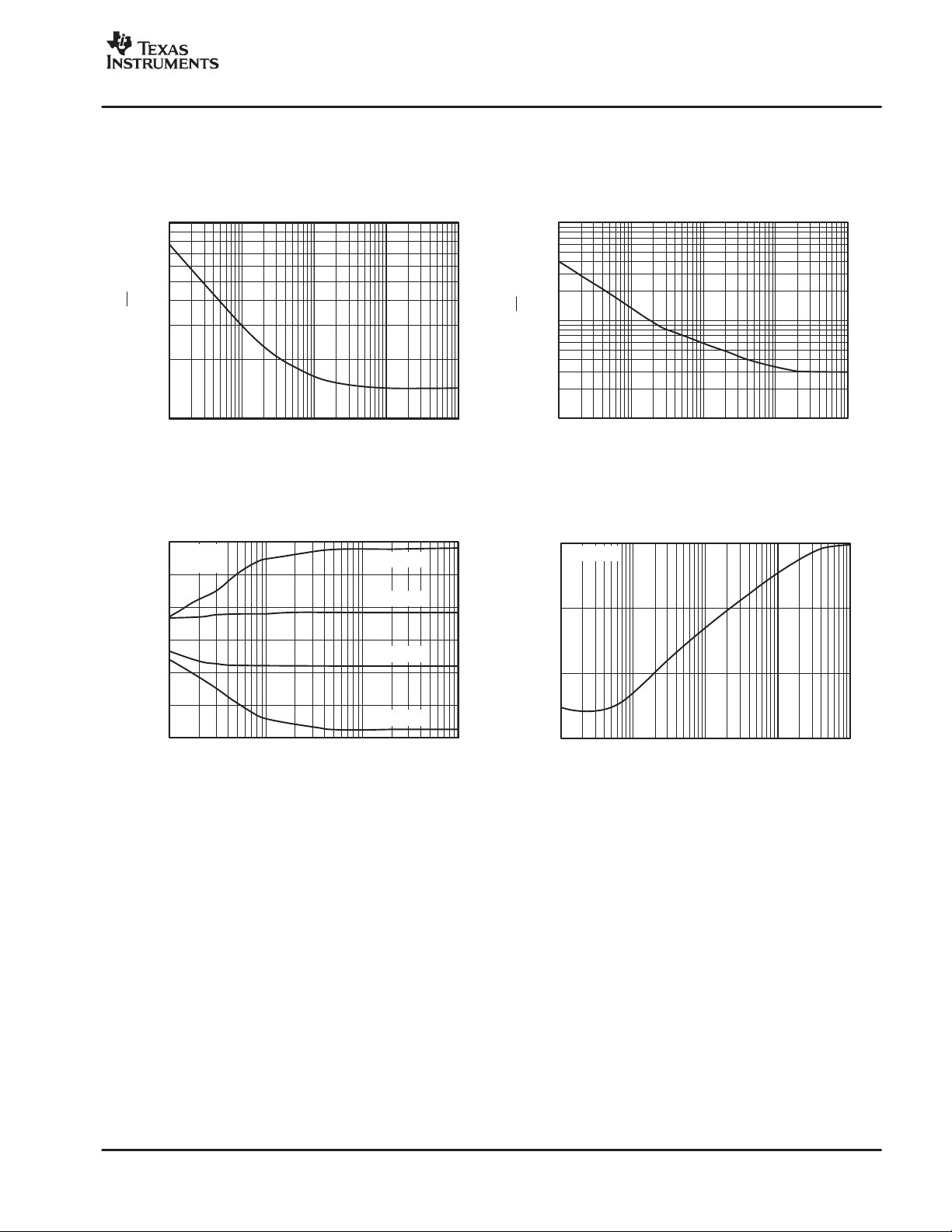
TYPICAL CHARACTERISTICS
At TA = +25°C, VS = ±15V, and RL = 2kΩ, unless otherwise noted.
www.ti.com
0.001
Gain= +1
= 348
R
F
=3Vrms
V
O
Differential I/O
0.0001
THD + Noise (%)
0.00001
RL=600
RL=2k
10 100 1k 10k 100k
0.1
Gain = +1
R
F
f=1kHz
0.01
Differential I/O
0.001
THD + NOISE vs FREQUENCY
Ω
Ω
Ω
Frequency (Hz)
THD + NOISE vs OUTPUT VOLTAGE
Ω
=348
RL= 600
0.001
Gain = +1
RF=348
VO=3Vrms
Single−Ended Input
Differential Output
0.0001
THD + Noise (%)
0.00001
Ω
RL=600
RL=2k
10 100 1k 10k 100k
0.01
0.001
THD + NOISE vs FREQUENCY
Ω
Ω
Ω
Frequency (Hz)
THD + NOISE vs OUTPUT VOLTAGE
RL= 600
Ω
THD + Noise (%)
0.0001
0.00001
0.01 0.1 1 10 100
Differential Output Voltage (Vrms)
INTERMODULATION DISTORTION
0.1
0.01
0.001
IMD(%)
0.0001
0.00001
Gain = +1
=348
R
F
Differential I/O
SMPTE 4:1; 60Hz, 7kHz
DIN 4:1; 250Hz, 8kHz
0.01 0.1 1 10 100
vs OUTPUT VOLTAGE
Ω
Differential Output Voltage (V
RL=600
PP
)
RL=2k
Ω
RL=2k
Ω
Ω
0.0001
THD + Noise (%)
0.00001
IMD(%)
0.0001
0.00001
Gain = +1
Ω
=348
R
F
f=1kHz
Single−Ended Input
Differential Output
0.01 0.1 1 10 100
Differential Output Voltage (Vrms)
INTERMODULATION DISTORTION
0.1
0.01
0.001
Gain = +1
=348
R
F
Single−Ended Input
Differential Output
SMPTE 4:1; 60Hz, 7kHz
DIN 4:1; 250Hz, 8kHz
0.01 0.1 1 10 100
vs OUTPUT VOLTAGE
Ω
Differential Output Voltage (V
RL= 600
)
PP
RL=2k
Ω
RL=2k
Ω
Ω
4
Page 5
www.ti.com
TYPICAL CHARACTERISTICS (Cont.)
At TA = +25°C, VS = ±15V, and RL = 2kΩ, unless otherwise noted.
"#$%
SBOS286A − DECEMBER 2003 − REVISED SEPTEMBER 2006
10
Hz)
√
(nV/
n
V
1
10 100 1k 10k 100k
15
RF=1k
G=+2
10
5
(V)
0
O
V
−
5
−
10
−
15
100 1k 10k 100k
VOLTAGE NOISE vs FREQUENCY
Frequency (Hz)
vs DIFFERENTIAL LOAD RESISTANCE
Ω
OUTPUT VOLTAGE
(Ω)
R
L
VCC=±15V
VCC=±5V
VCC=±5V
VCC=±15V
10
Hz)
√
1
(pA/
n
I
0.1
10 100 1k 10k 100k
100
VCC=±5V
)
Ω
10
1
Output Impedance (
0.1
100k 1M 10M 100M 1G
CURRENT NOISE vs FREQUENCY
Frequency (Hz)
OUTPUT IMPEDANCE
vs FREQUENCY
Frequency (Hz)
5
Page 6

"#$%
SBOS286A − DECEMBER 2003 − REVISED SEPTEMBER 2006
www.ti.com
APPLICATIONS INFORMATION
Figure 1 shows the OPA1632 used as a differential-output
driver for the PCM1804 high-performance audio ADC.
Supply voltages of ±15V are commonly used for the
OPA1632. The relatively low input voltage swing required
by the ADC allows use of lower power-supply voltage, if
desired. Power supplies as low as ±8V can be used in this
application with excellent performance. This reduces
power dissipation and heat rise. Power supplies should be
bypassed with 10µF tantalum capacitors in parallel with
0.1µF ceramic capacitors to avoid possible oscillations
and instability.
The V
provides the proper input common-mode reference
voltage (2.5V). This V
and drives the output common-mode voltage pin of the
A
2
OPA1632. This biases the average output voltage of the
OPA1632 to 2.5V.
The signal gain of the circuit is generally set to
approximately 0.25 to be compatible with commonly-used
audio line levels. Gain can be adjusted, if necessary, by
reference voltage output on the PCM1804 ADC
COM
voltage is buffered with op amp
COM
+8V to +16V
changing the values of R
values (R
and R4) should be kept relatively low, as
3
and R2. The feedback resistor
1
indicated, for best noise performance.
R
, R6, and C3 provide an input filter and charge glitch
5
reservoir for the ADC. The values shown are generally
satisfactory. Some adjustment of the values may help
optimize performance with different ADCs.
It is important to maintain accurate resistor matching on
and R3/R4 to achieve good differential signal
R
1/R2
balance. Use 1% resistors for highest performance. When
connected for single-ended inputs (inverting input
grounded, as shown in Figure 1), the source impedance
must be low. Differential input sources must have
well-balanced or low source impedance.
Capacitors C
, C2, and C3 should be chosen carefully for
1
good distortion performance. Polystyrene, polypropylene,
NPO ceramic, and mica types are generally excellent.
Polyester and high-K ceramic types such as Z5U can
create distortion.
V+
10µF
+
R
1
Ω
1k
Input
+
−
Enable
R
2
Ω
1k
(1)
Balancedor
Single−Ended
NOTE: (1) Leave open to enable.
Logic signals referenced to V−supply.
See the Shutdown Function section.
0.1µF
R
3
Ω
270
C
1
1nF
R
5
R
4
Ω
OPA134
40
40
Ω
C
3
2.7nF
R
6
Ω
Ω
1k
0.1µF
1/2
PCM1804
V
COM
(2.5V)
3
8
V
OCM
2
1
0.1µF
10µF
+
OPA1632
6
7
−
8V to−16V
−
V
5
4
C
1nF
2
270
Figure 1. ADC Driver for Professional Audio
6
Page 7

www.ti.com
"#$%
SBOS286A − DECEMBER 2003 − REVISED SEPTEMBER 2006
FULLY-DIFFERENTIAL AMPLIFIERS
Differential signal processing offers a number of
performance advantages in high-speed analog signal
processing systems, including immunity to external
common-mode noise, suppression of even-order
nonlinearities, and increased dynamic range. Fully-differential amplifiers not only serve as the primary means
of providing gain to a differential signal chain, but also
provide a monolithic solution for converting single-ended signals into differential signals allowing for easy,
high-performance processing.
A standard configuration for the device is shown in
Figure 2. The functionality of a fully differential amplifier
can be imagined as two inverting amplifiers that share
a common noninverting terminal (though the voltage is
not necessarily fixed). For more information on the
basic theory of operation for fully differential amplifiers,
refer to the Texas Instruments application note
SLOA054, Fully Differential Amplifiers, available for
download from the TI web site (www.ti.com).
+15V
V
IN+
V
V
−
IN
OCM
A
IN
A
IN
Digital
Output
V
REF
Quiescent current is reduced to approximately 0.85mA
when the amplifier is disabled. When disabled, the
output stage is not in a high-impedance state. Thus, the
shutdown function cannot be used to create a
multiplexed switching function in series with multiple
amplifiers.
OUTPUT COMMON-MODE VOLTAGE
The output common-mode voltage pin sets the DC
output voltage of the OPA1632. A voltage applied to the
V
pin from a low-impedance source can be used to
OCM
directly set the output common-mode voltage. For a
V
voltage at mid-supply , make no connection to the
OCM
V
pin.
OCM
Depending on the intended application, a decoupling
capacitor is recommended on the V
any high-frequency noise that could couple into the
signal path through the V
circuitry. A 0.1µF or 1µF
OCM
capacitor is generally adequate.
Output common-mode voltage causes additional
current to flow in the feedback resistor network. Since
this current is supplied by the output stage of the
amplifier, this creates additional power dissipation. For
commonly-used feedback resistance values, this
current is easily supplied by the amplifier . The additional
internal power dissipation created by this current may
be significant in some applications and may dictate use
of the MSOP PowerPAD package to effectively control
self-heating.
node to filter
OCM
−
15V
Figure 2. Typical ADC Circuit
SHUTDOWN FUNCTION
The shutdown (enable) function of the OPA1632 is
referenced to the negative supply of the operational
amplifier. A valid logic low (< 0.8V above negative
supply) applied to the enable pin (pin 7) disables the
amplifier output. Voltages applied to pin 7 that are
greater than 2V above the negative supply place the
amplifier output in an active state, and the device is
enabled. If pin 7 is left disconnected, an internal pull-up
resistor enables the device. Turn-on and turn-off times
are approximately 2µs each.
PowerPAD DESIGN CONSIDERATIONS
The OPA1632 is available in a thermally-enhanced
PowerPAD family of packages. These packages are
constructed using a downset leadframe upon which the
die is mounted (see Figure 3[a] and Figure 3[b]). This
arrangement results in the lead frame being exposed as
a thermal pad on the underside of the package (see
Figure 3[c]). Because this thermal pad has direct
thermal contact with the die, excellent thermal
performance can be achieved by providing a good
thermal path away from the thermal pad.
DIE
(a) Side View
DIE
(b) End View
Figure 3. Views of th e Thermall y-En h an ced Package.
Thermal
Pad
(c) Bottom View
7
Page 8

"#$%
SBOS286A − DECEMBER 2003 − REVISED SEPTEMBER 2006
www.ti.com
The PowerPAD package allows for both assembly and
thermal management in one manufacturing operation.
During the surface-mount solder operation (when the
leads are being soldered), the thermal pad must be
soldered to a copper area underneath the package.
Through the use of thermal paths within this copper
area, heat can be conducted away from the package
into either a ground plane or other heat-dissipating
device. Soldering the PowerPAD to the printed circuit
board (PCB) is always required, even with applications
that have low power dissipation. It provides the
necessary thermal and mechanical connection
between the lead frame die pad and the PCB.
PowerPAD PCB LAYOUT CONSIDERATIONS
1. The thermal pad must be connected to the most
negative supply voltage on the device, V−.
2. Prepare the PCB with a top-side etch pattern, as
shown in Figure 4. There should be etch for the
leads as well as etch for the thermal pad.
Single or Dual
68mils x 70mils
(via diameter = 13mils)
These vias help dissipate the heat generated by the
OPA1632 IC, and may be larger than the 13mil
diameter vias directly under the thermal pad. They
can be larger because they are not in the thermal
pad area to be soldered so that wicking is not a
problem.
5. Connect all holes to the internal power plane that is
at the same voltage potential as V−.
6. When connecting these holes to the plane, do not
use the typical web or spoke via connection
methodology. Web connections have a high
thermal resistance connection that is useful for
slowing the heat transfer during soldering
operations. This makes the soldering of vias that
have plane connections easier. In this application,
however, low thermal resistance is desired for the
most efficient heat transfer. Therefore, the holes
under the OPA1632 PowerPAD package should
make their connection to the internal plane with a
complete connection around the entire
circumference of the plated-through hole.
7. The top-side solder mask should leave the terminals
of the package and the thermal pad area with its five
holes exposed. The bottom-side solder mask should
cover the five holes of the thermal pad area. This
prevents solder from being pulled away from the
thermal pad area during the reflow process.
Figure 4. PowerPAD PCB Etch and Via Pattern.
3. Place five holes in the area of the thermal pad.
These holes should be 13mils in diameter. Keep
them small so that solder wicking through the holes
is not a problem during reflow.
4. Additional vias may be placed anywhere along the
thermal plane outside of the thermal pad area.
8. Apply solder paste to the exposed thermal-pad
area and all of the IC terminals.
9. With these preparatory steps in place, the IC is
simply placed in position and runs through the
solder reflow operation as any standard
surface-mount component. This results in a part
that is properly installed.
8
Page 9
www.ti.com
"#$%
SBOS286A − DECEMBER 2003 − REVISED SEPTEMBER 2006
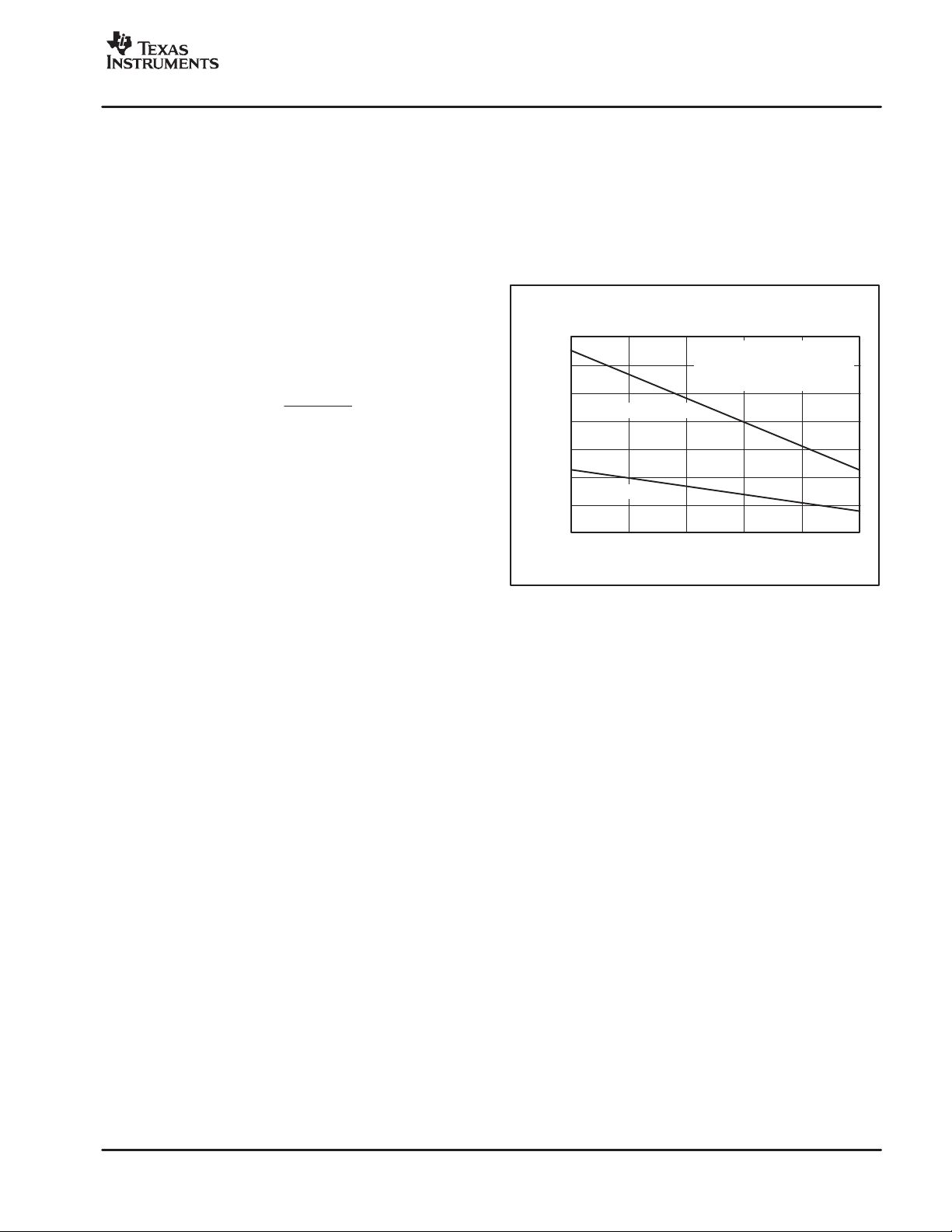
POWER DISSIPATION AND THERMAL
CONSIDERATIONS
The OPA1632 does not have thermal shutdown
protection. Take care to assure that the maximum
junction temperature is not exceeded. Excessive
junction temperature can degrade performance or
cause permanent damage. For best performance and
reliability, assure that the junction temperature does not
exceed +125°C.
The thermal characteristics of the device are dictated
by the package and the circuit board. Maximum power
dissipation for a given package can be calculated using
the following formula:
T
* T
+
max
P
Dmax
Where:
P
is the maximum power dissipation in the
Dmax
amplifier (W).
T
is the absolute maximum junction
max
temperature (_C).
TA is the ambient temperature (_C).
q
= qJC + q
JA
q
is the thermal coefficient from the silicon
JC
CA.
junctions to the case (_C/W).
q
is the thermal coefficient from the case to
CA
ambient air (_C/W).
A
q
JA
(1)
For systems where heat dissipation is more critical, the
OPA1632 is offered in an MSOP-8 with PowerPAD.
The thermal coefficient for the MSOP PowerPAD
(DGN) package is substantially improved over the
traditional SO package. Maximum power dissipation
levels are depicted in Figure 5 for the two packages.
The data for the DGN package assumes a board layout
that follows the PowerPAD layout guidelines.
MAXIMUM POWER DISSIPATION
3.5
3.0
2.5
MSOP−8 (DGN) Package
2.0
1.5
1.0
SO−8 (D) Package
0.5
Maximum Power Dissipation (W)
0
−
40
vs AMBIENT TEMPERATURE
θ
= 170_C/W forSO −8 (D)
JA
θ
= 58.4_C/W for MSOP−8 (DGN)
JA
TJ= 150_C
NoAirflow
−
15 10 856035
Ambient Temperature (_C)
Figure 5. Maximum Power Dissipation vs Ambient
Temperature
9
Page 10

PACKAGE OPTION ADDENDUM
www.ti.com
12-Sep-2006
PACKAGING INFORMATION
Orderable Device Status
(1)
Package
Type
Package
Drawing
Pins Package
Qty
Eco Plan
OPA1632D ACTIVE SOIC D 8 75 Green (RoHS &
no Sb/Br)
OPA1632DG4 ACTIVE SOIC D 8 75 Green (RoHS &
no Sb/Br)
OPA1632DGN ACTIVE MSOP-
Power
DGN 8 80 Green (RoHS&
no Sb/Br)
PAD
OPA1632DGNG4 ACTIVE MSOP-
Power
DGN 8 80 Green (RoHS&
no Sb/Br)
PAD
OPA1632DGNR ACTIVE MSOP-
Power
DGN 8 2500 Green (RoHS &
no Sb/Br)
PAD
OPA1632DGNRG4 ACTIVE MSOP-
Power
DGN 8 2500 Green (RoHS &
no Sb/Br)
PAD
OPA1632DR ACTIVE SOIC D 8 2500 Green (RoHS &
no Sb/Br)
OPA1632DRG4 ACTIVE SOIC D 8 2500 Green (RoHS &
no Sb/Br)
(1)
The marketing status valuesare defined as follows:
ACTIVE: Product device recommendedfor new designs.
LIFEBUY: TI has announcedthat the device will be discontinued, and a lifetime-buy period is in effect.
NRND: Not recommended for new designs. Device is in production to support existing customers, but TI does not recommend using this part in
a new design.
PREVIEW: Device has beenannounced but is not in production. Samples may or may not be available.
OBSOLETE: TI has discontinuedthe production of the device.
(2)
Lead/Ball Finish MSL Peak Temp
CU NIPDAU Level-1-260C-UNLIM
CU NIPDAU Level-1-260C-UNLIM
CU NIPDAU Level-1-260C-UNLIM
CU NIPDAU Level-1-260C-UNLIM
CU NIPDAU Level-1-260C-UNLIM
CU NIPDAU Level-1-260C-UNLIM
CU NIPDAU Level-1-260C-UNLIM
CU NIPDAU Level-1-260C-UNLIM
(3)
(2)
Eco Plan - The planned eco-friendly classification: Pb-Free (RoHS), Pb-Free (RoHS Exempt), or Green (RoHS & no Sb/Br) - please check
http://www.ti.com/productcontent for the latestavailability information and additional product content details.
TBD: The Pb-Free/Green conversionplan has not been defined.
Pb-Free (RoHS): TI's terms "Lead-Free" or "Pb-Free" mean semiconductor products that are compatible with the current RoHS requirements
for all 6 substances, including the requirement that lead not exceed 0.1% by weight in homogeneous materials. Where designed to be soldered
at high temperatures, TIPb-Free products are suitable for use in specified lead-free processes.
Pb-Free (RoHS Exempt): This component has a RoHS exemption for either 1) lead-based flip-chip solder bumps used between the die and
package, or 2) lead-based die adhesive used between the die and leadframe. The component is otherwise considered Pb-Free (RoHS
compatible) as defined above.
Green (RoHS & no Sb/Br): TI defines "Green" to mean Pb-Free (RoHS compatible), and free of Bromine (Br) and Antimony (Sb) based flame
retardants (Br or Sbdo not exceed 0.1% by weight in homogeneous material)
(3)
MSL, Peak Temp. -- The Moisture Sensitivity Level rating according to the JEDEC industry standard classifications, and peak solder
temperature.
Important Information and Disclaimer:The information provided on this page represents TI's knowledge and belief as of the date that it is
provided. TI bases its knowledge and belief on information provided by third parties, and makes no representation or warranty as to the
accuracy of such information. Efforts are underway to better integrate information from third parties. TI has taken and continues to take
reasonable steps to provide representative and accurate information but may not have conducted destructive testing or chemical analysis on
incoming materials and chemicals. TI and TI suppliers consider certain information to be proprietary, and thus CAS numbers and other limited
information may not beavailable for release.
In no event shall TI's liability arising out of such information exceed the total purchase price of the TI part(s) at issue in this document sold by TI
to Customer on anannual basis.
Addendum-Page 1
Page 11

PACKAGE MATERIALS INFORMATION
www.ti.com
23-May-2007
TAPE AND REEL INFORMATION
Pack Materials-Page 1
Page 12

PACKAGE MATERIALS INFORMATION
www.ti.com
Device Package Pins Site Reel
Diameter
(mm)
OPA1632DGNR DGN 8 LEN 330 12 5.2 3.3 1.6 8 12 NONE
OPA1632DR D 8 TAI 330 12 6.4 5.2 2.1 8 12 Q1
Reel
Width
(mm)
A0 (mm) B0 (mm) K0 (mm) P1
(mm)W(mm)
23-May-2007
Pin1
Quadrant
TAPE AND REEL BOX INFORMATION
Device Package Pins Site Length (mm) Width (mm) Height (mm)
OPA1632DGNR DGN 8 LEN 566.0 340.5 21.1
OPA1632DR D 8 TAI 346.0 346.0 29.0
Pack Materials-Page 2
Page 13

Page 14

Page 15

Page 16

IMPORTANT NOTICE
Texas Instruments Incorporated and its subsidiaries (TI) reserve the right to make corrections, modifications, enhancements,
improvements, and other changes to its products and services at any time and to discontinue any product or service without notice.
Customers should obtain the latest relevant information before placing orders and should verify that such information is current and
complete. All products are sold subject to TI’s terms and conditions of sale supplied at the time of order acknowledgment.
TI warrants performance of its hardware products to the specifications applicable at the time of sale in accordance with TI’s
standard warranty. Testing and other quality control techniques are used to the extent TI deems necessary to support this
warranty. Except where mandated by government requirements, testing of all parameters of each product is not necessarily
performed.
TI assumes no liability for applications assistance or customer product design. Customers are responsible for their products and
applications using TI components. To minimize the risks associated with customer products and applications, customers should
provide adequate design and operating safeguards.
TI does not warrant or represent that any license, either express or implied, is granted under any TI patent right, copyright, mask
work right, or other TI intellectual property right relating to any combination, machine, or process in which TI products or services
are used. Information published by TI regarding third-party products or services does not constitute a license from TI to use such
products or services or a warranty or endorsement thereof. Use of such information may require a license from a third party under
the patents or other intellectual property of the third party, or a license from TI under the patents or other intellectual property of TI.
Reproduction of TI information in TI data books or data sheets is permissible only if reproduction is without alteration and is
accompanied by all associated warranties, conditions, limitations, and notices. Reproduction of this information with alteration is an
unfair and deceptive business practice. TI is not responsible or liable for such altered documentation. Information of third parties
may be subject to additional restrictions.
Resale of TI products or services with statements different from or beyond the parameters stated by TI for that product or service
voids all express and any implied warranties for the associated TI product or service and is an unfair and deceptive business
practice. TI is not responsible or liable for any such statements.
TI products are not authorized for use in safety-critical applications (such as life support) where a failure of the TI product would
reasonably be expected to cause severe personal injury or death, unless officers of the parties have executed an agreement
specifically governing such use. Buyers represent that they have all necessary expertise in the safety and regulatory ramifications
of their applications, and acknowledge and agree that they are solely responsible for all legal, regulatory and safety-related
requirements concerning their products and any use of TI products in such safety-critical applications, notwithstanding any
applications-related information or support that may be provided by TI. Further, Buyers must fully indemnify TI and its
representatives against any damages arising out of the use of TI products in such safety-critical applications.
TI products are neither designed nor intended for use in military/aerospace applications or environments unless the TI products are
specifically designated by TI as military-grade or "enhanced plastic." Only products designated by TI as military-grade meet military
specifications. Buyers acknowledge and agree that any such use of TI products which TI has not designated as military-grade is
solely at the Buyer's risk, and that they are solely responsible for compliance with all legal and regulatory requirements in
connection with such use.
TI products are neither designed nor intended for use in automotive applications or environments unless the specific TI products
are designated by TI as compliant with ISO/TS 16949 requirements. Buyers acknowledge and agree that, if they use any
non-designated products in automotive applications, TI will not be responsible for any failure to meet such requirements.
Following are URLs where you can obtain information on other Texas Instruments products and application solutions:
Products Applications
Amplifiers amplifier.ti.com Audio www.ti.com/audio
Data Converters dataconverter.ti.com Automotive www.ti.com/automotive
DSP dsp.ti.com Broadband www.ti.com/broadband
Interface interface.ti.com Digital Control www.ti.com/digitalcontrol
Logic logic.ti.com Military www.ti.com/military
Power Mgmt power.ti.com Optical Networking www.ti.com/opticalnetwork
Microcontrollers microcontroller.ti.com Security www.ti.com/security
RFID www.ti-rfid.com Telephony www.ti.com/telephony
Low Power www.ti.com/lpw Video & Imaging www.ti.com/video
Wireless
Wireless www.ti.com/wireless
Mailing Address: Texas Instruments, Post Office Box 655303, Dallas, Texas 75265
Copyright © 2007, Texas Instruments Incorporated
 Loading...