

Page 1
®
OPA128
Difet
®
Electrometer-Grade
OPERATIONAL AMPLIFIER
FEATURES
● ULTRA-LOW BIAS CURRENT: 75fA max
● LOW OFFSET: 500µV max
● LOW DRIFT: 5µV/
● HIGH OPEN-LOOP GAIN: 110dB min
● HIGH COMMON-MODE REJECTION:
90dB min
● IMPROVED REPLACEMENT FOR AD515
AND AD549
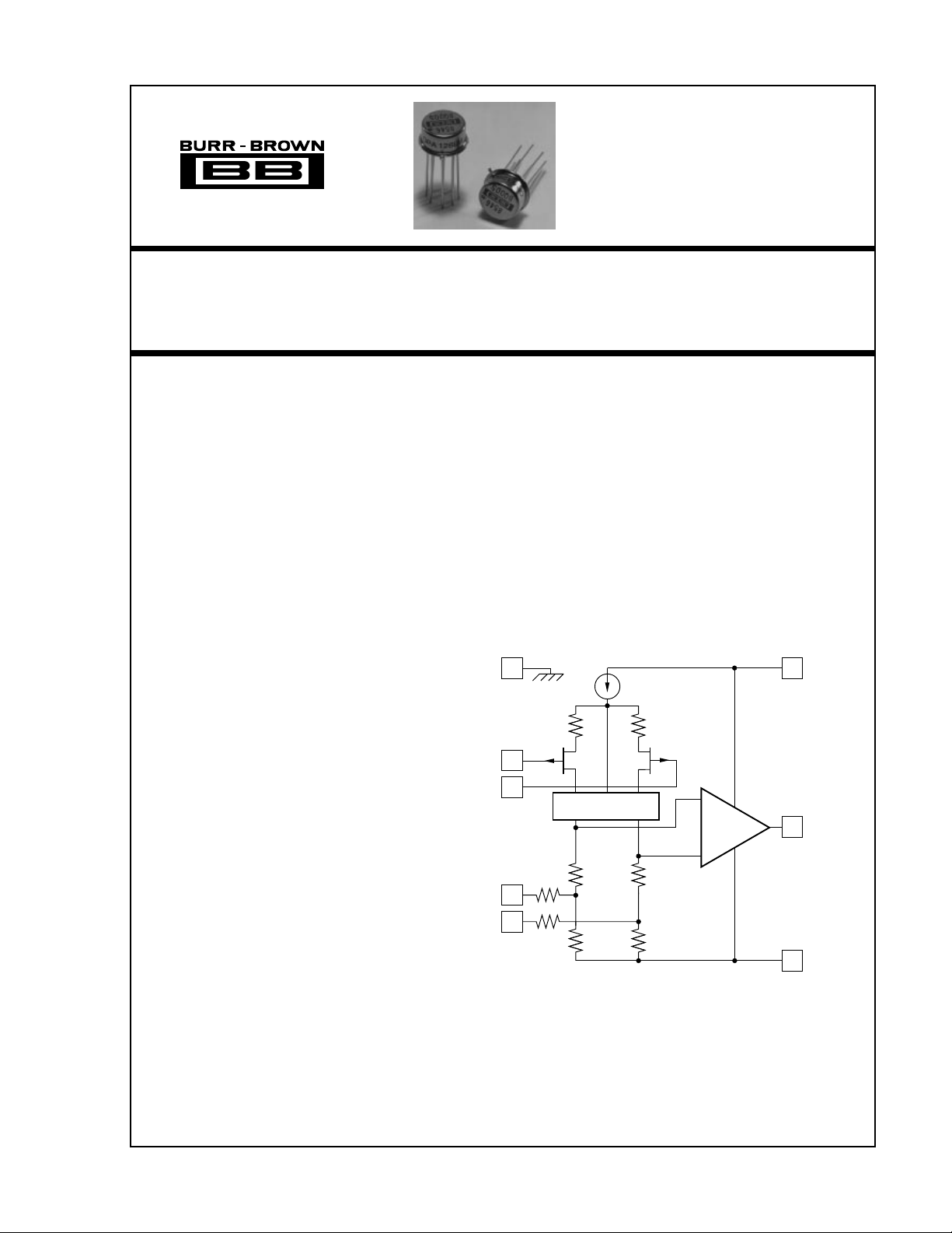
DESCRIPTION
The OPA128 is an ultra-low bias current monolithic
operational amplifier. Using advanced geometry
dielectrically-isolated FET (
lithic amplifier achieves a performance level exceeding even the best hybrid electrometer amplifiers.
Laser-trimmed thin-film resistors give outstanding voltage offset and drift performance.
A noise-free cascode and low-noise processing give
the OPA128 excellent low-level signal handling capabilities. Flicker noise is very low.
The OPA128 is an improved pin-for-pin replacement
for the AD515.
®
Difet
Burr-Brown Corp.
°C max
Difet
®
) inputs, this mono-
APPLICATIONS
● ELECTROMETER
● MASS SPECTROMETER
● CHROMATOGRAPH
● ION GAUGE
● PHOTODETECTOR
● RADIATION-HARD EQUIPMENT
Case (Guard)
8
–In
2
3
+In
Trim
1
5
Trim
Noise-Free
Cascode
28kΩ
Ω1k
Ω1k
2kΩ 2kΩ
OPA128 Simplified Circuit
28kΩ
7
+V
CC
6
Output
4
–V
CC
International Airport Industrial Park • Mailing Address: PO Box 11400 • Tucson, AZ 85734 • Street Address: 6730 S. Tucson Blvd. • Tucson, AZ 85706
Tel: (520) 746-1111 • Twx: 910-952-1111 • Cable: BBRCORP • Telex: 066-6491 • FAX: (520) 889-1510 • Immediate Product Info: (800) 548-6132
©
1986 Burr-Brown Corporation PDS-653E Printed in U.S.A. May, 1995
Page 2
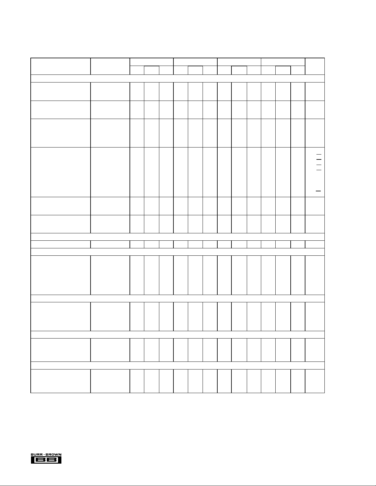
SPECIFICATIONS
ELECTRICAL
At V
= ±15VDC and TA = +25°C unless otherwise noted. Pin 8 connected to ground.
CC
OPA128JM OPA128KM OPA128LM OPA128SM
PARAMETER CONDITIONS MIN TYP MAX MIN TYP MAX MIN TYP MAX MIN TYP MAX UNITS
INPUT
BIAS CURRENT
Input Bias Current VCM = 0VDC,
OFFSET CURRENT
Input Offset Current VCM = 0VDC,
OFFSET VOLTAGE
Input Offset Voltage VCM = 0VDC ±260 ±1000 ±140 ±500 ±140 ±500 ±140 ±500 µV
Average Drift T
Supply Rejection 80 120 90 120 90 120 90 120 dB
NOISE
Voltage: f
f
f
f
f
f
Current: f
f
IMPEDANCE
Differential 10
Common-Mode 10
VOLTAGE RANGE
Common-Mode Input Range ±10 ±12 ±10 ±12 ±10 ±12 ±10 ±12 V
Common-Mode Rejection V
OPEN-LOOP GAIN, DC
Open-Loop Voltage Gain R
FREQUENCY RESPONSE
Unity Gain, Small Signal
Full Power Response 20Vp-p, R
Slew Rate V
Settling Time, 0.1% Gain = –1, R
0.01% 10V Step 10 10 10 10 µs
Overload Recovery,
50% Overdrive
RATED OUTPUT
Voltage Output R
Current Output V
Output Resistance DC, Open Loop 100 100 100 100 Ω
Load Capacitance Stability Gain = +1 1000 1000 1000 1000 pF
Short Circuit Current 10 34 55 10 34 55 10 34 55 10 34 55 mA
POWER SUPPLY
Rated Voltage ±15 ±15 ±15 ±15 VDC
Voltage Range,
Derated Performance ±5 ±18 ±5 ±18 ±5 ±18 ±5 ±18 VDC
Current, Quiescent I
TEMPERATURE RANGE
Specification Ambient Temp. 0 +70 0 +70 0 +70 –55 +125 °C
Operating Ambient Temp. –55 +125 –55 +125 –55 +125 –55 +125 °C
Storage Ambient Temp. –65 +150 –65 +150 –65 +150 –65 +150 °C
θ
Junction-Ambient 200 200 200 200 ° C/W
NOTES: (1) Offset voltage, offset current, and bias current are measured with the units fully warmed up. Bias current doubles approximately every 11°C. (2) Sample
tested. (3) Overload recovery is defined as the time required for the output to return from saturation to linear operation following the removal of a 50% input overdrive.
(4) If it is possible for the input voltage to exceed the supply voltage, a series protection resistor should be added to limit input current to 0.5mA. The input devices
can withstand overload currents of 0.3mA indefinitely without damage.
The information provided herein is believed to be reliable; however, BURR-BROWN assumes no responsibility for inaccuracies or omissions. BURR-BROWN assumes
no responsibility for the use of this information, and all use of such information shall be entirely at the user’s own risk. Prices and specifications are subject to change
without notice. No patent rights or licenses to any of the circuits described herein are implied or granted to any third party. BURR-BROWN does not authorize or warrant
any BURR-BROWN product for use in life support devices and/or systems.
(1)
R
≥ 10kΩ±150 ±300 ±75 ±150 ±40 ±75 ±75 ±150 fA
(1)
(1)
L
R
≥ 10kΩ 65 30 30 30 fA
L
= T
to T
A
MIN
MAX
±20 ±10 ±5 ±10 µV/°C
±1 ±100 ±1 ±32 ±1 ±32 ±1 ±32 µV/V
= 10Hz 92 92 92 92 nV/√Hz
O
= 100Hz 78 78 78 78 nV/√Hz
O
= 1kHz 27 27 27 27 nV/√Hz
O
= 10kHz 15 15 15 15 nV/√Hz
O
= 10Hz to 10kHz 2.4 2.4 2.4 2.4 µVrms
B
= 0.1Hz to 10Hz 4 4 4 4 µVp-p
B
= 0.1Hz to 10Hz 4.2 3 2.3 3 fA, p-p
B
= 0.1Hz to 20kHz 0.22 0.16 0.12 0.16 fA/√Hz
O
13
|| 1 1013 || 1 1013 || 1 1013 || 1 Ω || pF
15
|| 2 1015 || 2 1015 || 2 1015 || 2 Ω || pF
(4)
= ±10VDC 80 118 90 118 90 118 90 118 dB
IN
≥ 2kΩ 94 128 110 128 110 128 110 128 dB
L
(2)
= 2kΩ 47 47 47 47 kHz
L
= ±10V, RL = 2kΩ 0.53131313V/µs
O
(3)
L
Gain = –1 5 5 5 5 µs
= 2kΩ±10 ±13 ±10 ±13 ±10 ±13 ±10 ±13 V
L
= ±10VDC ±5 ±10 ±5 ±10 ±5 ±10 ±5 ±10 mA
O
= 0mADC 0.9 1.5 0.9 1.5 0.9 1.5 0.9 1.5 mA
O
0.5 1 0.5 1 0.5 1 0.5 1 MHz
= 2kΩ 5555µs
®
OPA128
2
Page 3
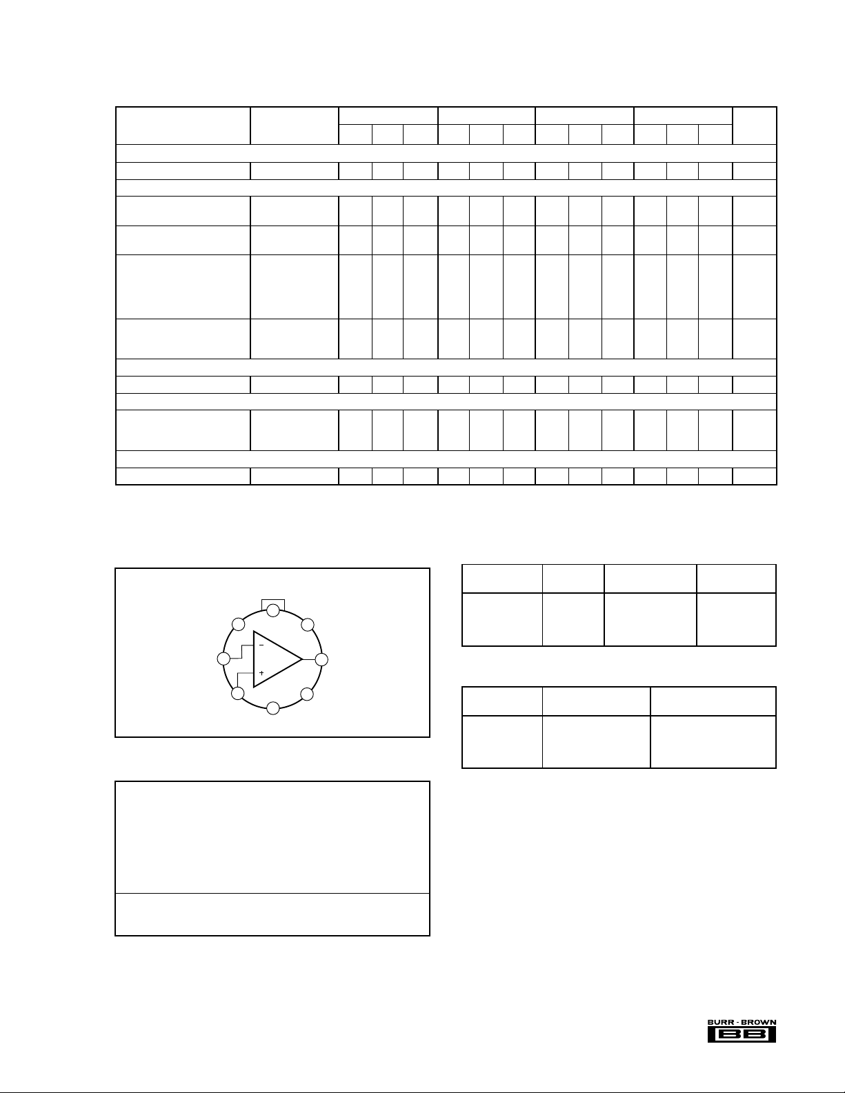
®
ELECTRICAL (FULL TEMPERATURE RANGE SPECIFICATIONS)
At V
= ±15VDC and TA = T
CC
PARAMETER CONDITIONS MIN TYP MAX MIN TYP MAX MIN TYP MAX MIN TYP MAX UNITS
TEMPERATURE RANGE
Specification Range Ambient Temp. 0 +70 0 +70 0 +70 –55 +125 °C
INPUT
BIAS CURRENT
(1)
Input Bias Current VCM = 0VDC ±2.5 ±8 ±1.3 ±4 ±0.7 ±2 ±43 ±170 pA
OFFSET CURRENT
Input Offset Current VCM = 0VDC 1.1 0.6 0.6 18 pA
OFFSET VOLTAGE
Input Offset Voltage VCM = 0VDC ±2.2mV ±1mV ±750 ±1.5mV µV
Average Drift ±20 ±10 ±5 ±10 µV/°C
Supply Rejection 74 114 80 114 80 114 80 106 dB
VOLTAGE RANGE
Common-Mode Input Range ±10 ±11 ±10 ±11 ±10 ±11 ±10 ±11 V
Commmon-Mode Rejection V
OPEN-LOOP GAIN, DC
Open-Loop Voltage Gain R
RATED OUTPUT
Voltage Output R
Current Output V
Short Circuit Current V
POWER SUPPLY
Current, Quiescent I = 0mADC 0.9 1.8 0.9 1.8 0.9 1.8 0.9 2 mA
NOTES: (1) Offset voltage, offset current, and bias current are measured with the units fully warmed up. (2) If it is possible for the input voltage to exceed the supply
voltage, a series protection resistor should be added to limit input current to 0.5mA. The input devices can withstand overload currents of 0.3mA indefinitely without
damage.
and T
MIN
unless otherwise noted.
MAX
OPA128JM OPA128KM OPA128LM OPA128SM
(1)
(1)
±2 ±200 ±2 ±100 ±2 ±100 ±5 ±100 µV/V
(2)
= ±10VDC 74 112 80 112 80 112 74 104 dB
IN
≥ 2kΩ 90 125 104 125 104 125 90 122 dB
L
= 2k±10 ±10 ±10 ±10 V
L
= ±10VDC ±5 ±5 ±5 ±5mA
O
= 0VDC 10 22 10 22 10 22 10 18 mA
O
CONNECTION DIAGRAM
Top View
Substrate and Case
Offset
Trim
2
–In
+In
1
3
8
OPA128
4
–V
CC
7
5
+V
CC
6
Offset
Trim
Output
ABSOLUTE MAXIMUM RATINGS
Supply ...........................................................................................±18VDC
Internal Power Dissipation
Differential Input Voltage...............................................................±36VDC
Input Voltage Range ..................................................................... ±18VDC
Storage Temperature Range .......................................... –65°C to +150°C
Operating Temperature Range ....................................... –55°C to +125°C
Lead Temperature (soldering, 10s)................................................ +300°C
Output Short Circuit Duration
Junction Temperature .................................................................... +175°C
NOTES: (1) Packages must be derated based on
200°C/W. (2) Short circuit may be to power supply common only. Rating
applies to +25°C ambient. Observe dissipation limit and T
(1)
..........................................................500mW
(2)
................................................ Continuous
θ
= 150°C/W or
CA
.
J
ORDERING INFORMATION
MODEL PACKAGE RANGE max (fA)
OPA128JM TO-99 0°C to +70°C ±300
OPA128KM TO-99 0°C to +70°C ±150
OPA128LM TO-99 0°C to +70°C ±75
OPA128SM TO-99 –55°C to +125°C ±150
TEMPERATURE BIAS CURRENT,
PACKAGE INFORMATION
MODEL PACKAGE NUMBER
PACKAGE DRAWING
OPA128JM TO-99 001
OPA128KM TO-99 001
OPA128LM TO-99 001
OPA128SM TO-99 001
NOTE: (1) For detailed drawing and dimension table, please see end of data
sheet, or Appendix D of Burr-Brown IC Data Book.
θ
=
JA
(1)
3
OPA128
Page 4

DICE INFORMATION
OPA128 DIE TOPOGRAPHY
PAD FUNCTION
1 Offset Trim
2 –In
3 +In
4–V
5 Offset Trim
6 Output
7+V
8 Substrate
NC No Connection
Substrate Bias: Isolated, normally connected to common.
CC
CC
MECHANICAL INFORMATION
MILS (0.001") MILLIMETERS
Die Size 96 x 71 ±5 2.44 x 1.80 ±0.13
Die Thickness 20 ±3 0.51 ±0.08
Min. Pad Size 4 x 4 0.10 x 0.10
Backing None
TYPICAL PERFORMANCE CURVES
TA = +25°C, ±15VDC, unless otherwise noted.
140
120
100
80
60
Voltage Gain (dB)
40
20
0
120
110
100
OPEN-LOOP FREQUENCY RESPONSE
Gain
Ø
Phase
Margin
∼
≈ 90°
∼
11k10 100 10k 100k 1M 10M
Frequency (Hz)
COMMON-MODE REJECTION
vs INPUT COMMON-MODE VOLTAGE
–45
–90
–135
Phase Shift (Degrees)
–180
140
120
100
Power Supply Rejection (dB)
140
120
100
80
POWER SUPPLY REJECTION vs FREQUENCY
80
60
40
20
0
11k10 100 10k 100k 1M 10M
–PSRR
Frequency (Hz)
COMMON-MODE REJECTION
vs FREQUENCY
+PSRR
90
80
Common-Mode Rejection (dB)
70
–15
–10 –5 0 5 10 15
Common-Mode Voltage (V)
®
OPA128
60
40
20
Common-Mode Rejection (dB)
0
11k10 100 10k 100k 1M 10M
4
Frequency (Hz)
Page 5

®
TYPICAL PERFORMANCE CURVES (CONT)
0 5 10 20
Supply Voltage (±V
CC
)
0
3
2
1
Gain-Bandwidth (MHz)
GAIN-BANDWIDTH AND SLEW RATE
vs SUPPLY VOLTAGE
15
Slew Rate (V/µs)
0
6
4
2
– Slew
+ Slew
100
–75 –50 –25 0 25 50 125
Ambient Temperature (°C)
140
130
120
110
PSR, CMR, Voltage Gain (dB)
OPEN-LOOP GAIN, PSR, AND CMR vs TEMPERATURE
75
100
PSR
CMR
A
OL
At TA = +25°C, +15VDC unless otherwise noted.
BIAS AND OFFSET CURRENT
100pA
10pA
1pA
100
10
Bias and Offset Current (fA)
1
–50 –25 0 25 50 75 125
GAIN-BANDWIDTH AND SLEW RATE
4
3
2
1
Gain-Bandwidth (MHz)
vs TEMPERATURE
SM
Ambient Temperature (°C)
vs TEMPERATURE
I
B
BIAS AND OFFSET CURRENT
10
1
I
OS
0.1
Normalized Bias and Offset Current
0.01
100
4
3
2
Slew Rate (V/µs)
1
vs INPUT COMMON-MODE VOLTAGE
–15 –10 –5 0 5 10 15
Common-Mode Voltage (V)
0
–75 –50 –25 0 25 50 125
Ambient Temperature (°C)
2
1.5
1
Supply Current (mA)
0.5
0
–75 –50 –25 0 25 50 125
SUPPLY CURRENT vs TEMPERATURE
Ambient Temperature (°C)
0
100
75
75
100
5
OPA128
Page 6

TYPICAL PERFORMANCE CURVES (CONT)
At TA = +25°C, +15VDC unless otherwise noted.
LARGE SIGNAL TRANSIENT RESPONSE
10
0
Output Voltage (V)
–10
5V
05025
Time (µs)
COMMON-MODE INPUT RANGE
vs SUPPLY VOLTAGE
15
10
5
Common-Mode Voltage (±V)
0
0 5 10 20
Supply Voltage (±V
5µs
5µs
15
)
CC
SMALL SIGNAL TRANSIENT RESPONSE
80
40
0
Output Voltage (mV)
–40
–80
100pA
10pA
1pA
100
Bias Current (fA)
10
20mV 1µs
0108642
Time (µs)
BIAS CURRENT
vs ADDITIONAL POWER DISSIPATION
KM
1
0 50 100 150 200 250 350
Additional Power Dissipation (mW)
300
1k
100
Voltage Density (nV/ Hz)
10
INPUT VOLTAGE NOISE SPECTRAL DENSITY
1 10 100 1k 10k 100k
Frequency (Hz)
®
OPA128
30
20
10
Output Voltage (Vp-p)
0
FULL-POWER OUTPUT vs FREQUENCY
1k 10k 1M
Frequency (Hz)
100k
6
Page 7

®
APPLICATIONS INFORMATION
OFFSET VOLTAGE ADJUSTMENT
The OPA128 offset voltage is laser-trimmed and will require
no further trim for most applications. As with most amplifiers, externally trimming the remaining offset can change
drift performance by about 0.3µV/°C for each 100µV of
adjusted effort. Note that the trim (Figure 1) is similar to
operational amplifiers such as HA-5180 and AD515. The
OPA128 can replace many other amplifiers by leaving the
external null circuit unconnected.
+V
CC
The amplifier case should be connected to any input shield or
guard via pin 8. This insures that the amplifier itself is fully
surrounded by guard potential, minimizing both leakage and
noise pickup (see Figure 2).
In
Non-Inverting
2
3
8
OPA128
Out
6
In
Buffer
2
OPA128
3
8
Out
6
7
2
6
1
(1)
NOTE: (1) 10kΩ to 1MΩ
Trim Potentiometer
(100kΩ Recommended)
±10mV Typical
Trim Range
3
OPA128
5
4
–V
CC
FIGURE 1. Offset Voltage Trim.
INPUT PROTECTION
Conventional monolithic FET operational amplifiers’ inputs
must be protected against destructive currents that can flow
when input FET gate-to-substrate isolation diodes are for-
®
ward-biased. Most BIFET
the loss of –V
.
CC
amplifiers can be destroyed by
Because of its dielectric isolation, no special protection is
needed on the OPA128. Of course, the differential and
common-mode voltage limits should be observed.
Static damage can cause subtle changes in amplifier input
characteristics without necessarily destroying the device. In
precision operational amplifiers (both bipolar and FET types),
this may cause a noticeable degradation of offset voltage and
drift.
Static protection is recommended when handling any precision IC operational amplifier.
GUARDING AND SHIELDING
As in any situation where high impedances are involved,
careful shielding is required to reduce “hum” pickup in input
leads. If large feedback resistors are used, they should also be
shielded along with the external input circuitry. Leakage
currents across printed circuit boards can easily exceed the
bias current of the OPA128. To avoid leakage problems, it is
recommended that the signal input lead of the OPA128 be
wired to a Teflon standoff. If the input is to be soldered
directly into a printed circuit board, utmost care must be used
in planning the board layout. A “guard” pattern should
completely surround the high impedance input leads and
should be connected to a low impedance point which is at the
signal input potential.
Inverting
In
2
OPA128
3
Out
6
8
BOARD LAYOUT
FOR INPUT GUARDING
Guard top and bottom of board.
Alternate: use Teflon
for sensitive input pins.
Teflon® E.I. Du Pont de Nemours & Co.
TO-99 Bottom View
5
4
3
2
1
®
standoff
6
7
8
FIGURE 2. Connection of Input Guard.
Triboelectric charge (static electricity generated by friction)
can be a troublesome noise source from cables connected to
the input of an electrometer amplifier. Special low-noise cable
will minimize this effect but the optimum solution is to mount
the signal source directly at the electrometer input with short,
rigid, wiring to preclude microphonic noise generation.
TESTING
Accurately testing the OPA128 is extremely difficult due to its
high level of performance. Ordinary test equipment may not
be able to resolve the amplifier’s extremely low bias current.
Inaccurate bias current measurements can be due to:
1. Test socket leakage
2. Unclean package
3. Humidity or dew point condensation
4. Circuit contamination from fingerprints or anti-static
treatment chemicals
5. Test ambient temperature
6. Load power dissipation
BIFET® National Semiconductor Corp.
7
OPA128
Page 8

500Ω 9.5kΩ
Guard
pH Probe
R
≈ 500MΩ
S
50mV Output
100kΩ
FIGURE 3. High Impedance (10
–In
+15V
8
2
OPA128
3
5
1
–15V
15
Ω) Amplifier.
3
2
7
6
4
Offset Trim
OPA128
R
F
Ω10k
1VDC
Output
6
FIGURE 4. Piezoelectric Transducer Charge Amplifier.
≈ 100fA
I
B
Gain = 100
CMRR ≈ 118dB
R
≈ 1015Ω
IN
2
Q∆
100pF
Ω25k Ω25k
C
10pF
F
R
2
3
11
11
F
8
OPA128
e= –∆Q/C
O
Ω10
Low Frequency Cutoff =
Rπ
1/(2
5
Ω10
6
FCF
Output
e
O
F
) = 0.16Hz
R
G
Ω202
+In
R
F
Ω10k
2
OPA128
3
6
Differential Voltage Gain = 1 + 2R
Ω25k
3
Ω25k
1
F/RG
FIGURE 5. FET Input Instrumentation Amplifier for Biomedical Applications.
1N914
10kΩ
(1)
6
1N914
NOTE: (1) Reverse polarity
for negative peak detection.
1MΩ
(1)
(1)
2N4117A
Input
10pF≈
2
OPA606
3
Burr-Brown
INA105
Differential
Amplifier
2
3
1000µF
Polystyrene
8
OPA128
6
Output
6
Output
100µV/s≈Droop
FIGURE 6. Low-Droop Positive Peak Detector.
®
OPA128
8
Page 9

®
<1pF to prevent gain peaking.
10
Ω
10
Silicon Detector Corp.
SD-020-11-21-011
0.01µF
+15V
Guard
2
3
1010Ω
+5V
Biased
Current
Transducer
0.1µF
8
7
OPA128
0.1µF
4
–15V
Circuit must be well shielded.
+15V
1000MΩ
2
Current
6
Output
5 x 10
9
V/W
Input
3
OPA128
18kΩ
6
8
VO = –1V/nA
2kΩ
Output
FIGURE 8. Current-to-Voltage Converter.FIGURE 7. Sensitive Photodiode Amplifier.
109Ω
2
OPA128
3
6
8
3
4
5
10
11
12
INA101HP
1
Output
14
5
6
7
REF101
4 1
8
FIGURE 9. Biased Current-to-Voltage Converter.
VO = 1mV/pA
+5V
9
OPA128
 Loading...