

Page 1
Low Cost Precision
Difet
®
OPERATIONAL AMPLIFIER
Difet
®
, Burr-Brown Corp.
BIFET
®
, National Semiconductor Corp.
OPA121
FEATURES
● LOW NOISE: 6nV/√Hz typ at 10kHz
● LOW BIAS CURRENT: 5pA max
● LOW OFFSET: 2mV max
● LOW DRIFT: 3
µV/°C typ
● HIGH OPEN-LOOP GAIN: 110dB min
● HIGH COMMON-MODE
REJECTION: 86dB min
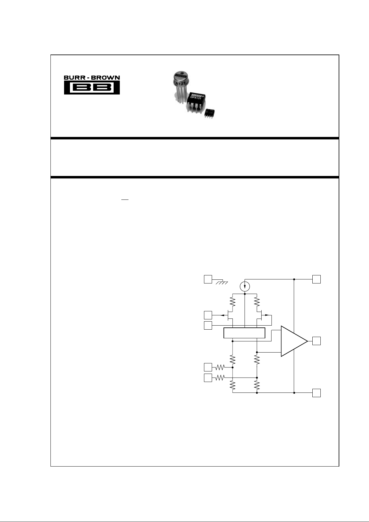
Noise-Free
Cascode*
Ω10k
Trim
1
5
3
2
+In
–In
Case (TO-99) and Substrate
Output
OPA121 Simplified Circuit
+V
CC
–V
CC
8
7
6
4
2kΩ
Ω10k
2kΩ
2kΩ
2kΩ
*Patented
Trim
DESCRIPTION
The OPA121 is a precision monolithic dielectricallyisolated FET (
Difet
®
) operational amplifier. Outstanding performance characteristics are now
available for low-cost applications.
Noise, bias current, voltage offset, drift, open-loop
gain, common-mode rejection, and power supply
rejection are superior to BIFET
®
amplifiers.
Very low bias current is obtained by dielectric
isolation with on-chip guarding.
Laser-trimming of thin-film resistors gives very low
offset and drift. Extremely low noise is achieved with
new circuit design techniques (patented). A new
cascode design allows high precision input specifications and reduced susceptibility to flicker noise.
Standard 741 pin configuration allows upgrading of
existing designs to higher performance levels.
APPLICATIONS
● OPTOELECTRONICS
● DATA ACQUISITION
● TEST EQUIPMENT
● MEDICAL EQUIPMENT
● RADIATION HARD EQUIPMENT
®
International Airport Industrial Park • Mailing Address: PO Box 11400 • Tucson, AZ 85734 • Street Address: 6730 S. Tucson Blvd. • Tucson, AZ 85706
Tel: (520) 746-1111 • Twx: 910-952-1111 • Cable: BBRCORP • Telex: 066-6491 • FAX: (520) 889-1510 • Immediate Product Info: (800) 548-6132
© 1984 Burr-Brown Corporation PDS-539F Printed in U.S.A. September, 1993
Page 2

®
OPA121
2
NOTES: (1) Sample tested. (2) Offset voltage, offset current, and bias current are specified with the units fully warmed up. (3) Overload recovery is defined as
the time required for the output to return from saturation to linear operation following the removal of a 50% input overdrive. (4) 100°C/W for KU grade.
SPECIFICATIONS
ELECTRICAL
At V
CC
= ±15VDC and TA = +25°C unless otherwise noted. Pin 8 connected to ground.
OPA121KM OPA121KP, KU
PARAMETER CONDITIONS MIN TYP MAX MIN TYP MAX UNITS
INPUT
NOISE
Voltage, f
O
= 10Hz
(1)
40 50 nV/√Hz
f
O
= 100Hz
(1)
15 18 nV/√Hz
f
O
= 1kHz
(1)
8 10 nV/√Hz
f
O
= 10kHz
(1)
6 7 nV/√Hz
f
B
= 10Hz to 10kHz
(1)
0.7 0.8 µVrms
f
B
= 0.1Hz to 10 Hz
(1)
1.6 2 µVp-p
Current, f
B
= 0.1Hz to 10Hz
(1)
15 21 fA, p-p
f
O
= 0.1Hz thru 20kHz
(1)
0.8 1.1 fA/√Hz
OFFSET VOLTAGE
(2)
Input Offset Voltage VCM = 0VDC ±0.5 ±2 ±0.5 ±3mV
Average Drift T
A
= T
MIN
to T
MAX
±3 ±10 ±3 ±10 µV/°C
Supply Rejection 86 104 86 104 dB
±6 ±50 ±6 ±50 µV/V
BIAS CURRENT
(2)
Input Bias Current VCM = 0VDC ±1 ±5 ±1 ±10 pA
Device Operating
OFFSET CURRENT
(2)
Input Offset Current VCM = 0VDC ±0.7 ±4 ±0.7 ±8pA
Device Operating
IMPEDANCE
Differential 10
13
|| 1 1013 || 1 Ω || pF
Common-Mode 10
14
|| 3 1014 || 3 Ω || pF
VOLTAGE RANGE
Common-Mode Input Range ±10 ±11 ±10 ±11 V
Common-Mode Rejection V
IN
= ±10VDC 86 104 82 100 dB
OPEN-LOOP GAIN, DC
Open-Loop Voltage Gain R
L
≥ 2kΩ 110 120 106 114 dB
FREQUENCY RESPONSE
Unity Gain, Small Signal 2 2 MHz
Full Power Response 20Vp-p, R
L
= 2kΩ 32 32 kHz
Slew Rate V
O
= ±10V, RL = 2kΩ 22V/µs
Settling Time, 0.1% Gain = –1, R
L
= 2kΩ 66µs
0.01% 10V Step 10 10 µs
Overload Recovery,
50% Overdrive
(3)
Gain = –1 5 5 µs
RATED OUTPUT
Voltage Output R
L
= 2kΩ±11 ±12 ±11 ±12 V
Current Output V
O
= ±10VDC ±5.5 ±10 ±5.5 ±10 mA
Output Resistance DC, Open Loop 100 100 Ω
Load Capacitance Stability Gain = +1 1000 1000 pF
Short Circuit Current 10 40 10 40 mA
POWER SUPPLY
Rated Voltage ±15 ±15 VDC
Voltage Range,
Derated Performance ±5 ±18 ±5 ±18 VDC
Current, Quiescent I
O
= 0mADC 2.5 4 2.5 4.5 mA
TEMPERATURE RANGE
Specification Ambient Temperature 0 +70 0 +70 °C
Operating Ambient Temperature –40 +85 –25 +85 °C
Storage Ambient Temperature –65 +150 –55 +125 °C
θ
Junction-Ambient 200 150
(4)
°C/W
The information provided herein is believed to be reliable; however, BURR-BROWN assumes no responsibility for inaccuracies or omissions. BURR-BROWN assumes
no responsibility for the use of this information, and all use of such information shall be entirely at the user’s own risk. Prices and specifications are subject to change
without notice. No patent rights or licenses to any of the circuits described herein are implied or granted to any third party. BURR-BROWN does not authorize or warrant
any BURR-BROWN product for use in life support devices and/or systems.
Page 3

®
OPA121
3
ELECTRICAL (FULL TEMPERATURE RANGE SPECIFICATIONS)
At VCC = ±15VDC and TA = T
MIN
to T
MAX
unless otherwise noted.
OPA121KM OPA121KP, KU
PARAMETER CONDITIONS MIN TYP MAX MIN TYP MAX UNITS
TEMPERATURE RANGE
Specification Range Ambient Temperature 0 +70 0 +70 °C
INPUT
OFFSET VOLTAGE
(1)
Input Offset Voltage VCM = 0VDC ±1 ±3 ±1 ±5mV
Average Drift ±3 ±10 ±3 ±10 µV/°C
Supply Rejection 82 94 82 94 dB
±20 ±80 ±20 ±80 µV/V
BIAS CURRENT
(1)
Input Bias Current VCM = 0VDC ±23 ±115 ±23 ±250 pA
Device Operating
OFFSET CURRENT
(1)
Input Offset Current VCM = 0VDC ±16 ±100 ±16 ±200 pA
Device Operating
VOLTAGE RANGE
Common-Mode Input Range ±10 ±11 ±10 ±11 V
Common-Mode Rejection V
IN
= ±10VDC 82 98 80 96 dB
OPEN-LOOP GAIN, DC
Open-Loop Voltage Gain R
L
≥ 2kΩ 106 116 100 110 dB
RATED OUTPUT
Voltage Output R
L
= 2kΩ±10.5 ±11 ±10.5 ±11 V
Current Output V
O
= ±10VDC ±5.25 ±10 ±5.25 ±10 mA
Short Circuit Current V
O
= 0VDC 10 40 10 40 mA
POWER SUPPLY
Current, Quiescent I
O
= 0mADC 2.5 4.5 2.5 5 mA
NOTE: (1) Offset voltage, offset current, and bias current are measured with the units fully warmed up.
PACKAGE INFORMATION
PACKAGE DRAWING
MODEL PACKAGE NUMBER
(1)
OPA121KM TO-99 001
OPA121KP 8-Pin Plastic DIP 006
OPA121KU 8-Pin SOIC 182
NOTE: (1) For detailed drawing and dimension table, please see end of data
sheet, or Appendix D of Burr-Brown IC Data Book.
CONNECTION DIAGRAMS
Top View M-Package TO-99 (Hermetic)
Top View P-Package Plastic Mini-DIP
U-Package Plastic SOIC
8
1
2
7
6
5
3
4
Offset
Trim
Offset
Trim
Output
+V
CC
Substrate and Case
–In
+In
OPA121
–V
CC
OPA121
1
2
3
4
5
6
7
8
Offset Trim
+V
CC
–In
+In
–V
CC
Output
Offset Trim
Substrate
TEMPERATURE
MODEL PACKAGE RANGE
OPA121KM TO-99 0°C to +70°C
OPA121KP 8-Pin Plastic DIP 0°C to +70°C
OPA121KU 8-Pin SOIC 0°C to +70°C
ORDERING INFORMATION
ABSOLUTE MAXIMUM RATINGS
Supply ........................................................................................... ±18VDC
Internal Power Dissipation
(1)
.........................................................500mW
Differential Input Voltage...............................................................±36VDC
Input Voltage Range ..................................................................... ±18VDC
Storage Temperature Range
M package .................................................................... –65°C to +150°C
P, U packages............................................................... –55°C to +125°C
Operating Temperature Range
M package ...................................................................... –40°C to +85°C
P, U packages................................................................. –25°C to +85°C
Lead Temperature
M, P packages (soldering, 10s) ...................................................+300°C
U package (soldering, 3s) ........................................................... +260°C
Output Short-Circuit Duration
(2)
............................................... Continuous
Junction Temperature .................................................................... +175°C
NOTES: (1) Packages must be derated based on
θ
JA
= 150°C/W
(P package);
θ
JA
= 200°C/W (M package);
θ
JA
= 100°C/W (U package).
(2) Short circuit may be to power supply common only. Rating applies to
+25°C ambient. Observe dissipation limit and T
J
.
Page 4

®
OPA121
4
11k10 100 10k 100k 1M 10M
Frequency (Hz)
0
20
40
60
80
100
120
140
Voltage Gain (dB)
OPEN-LOOP FREQUENCY RESPONSE
KM
–180
–135
–90
–45
Phase Shift (Degrees)
Phase
Margin
≈ 65°
Ø
Gain
∼
∼
11k10 100 10k 100k 1M 10M
Frequency (Hz)
0
20
40
60
80
100
120
140
Common-Mode Rejection (dB)
COMMON-MODE REJECTION
vs FREQUENCY
KM
11k10 100 10k 100k 1M 10M
Frequency (Hz)
0
20
40
60
80
100
120
140
Power Supply Rejection (dB)
POWER SUPPLY REJECTION
vs FREQUENCY
–15 –10 –5 0 +5 +10 +15
Common-Mode Voltage (V)
0.01
10
1
0.1
Bias Current (pA)
BIAS AND OFFSET CURRENT
vs INPUT COMMON-MODE VOLTAGE
0.01
10
1
0.1
Offset Current (pA)
Bias Current
Offset Current
KM
–50 –25 0 +25 +50 +75 +125
Ambient Temperature (°C)
0.01
1k
100
0.1
Bias Current (pA)
BIAS AND OFFSET CURRENT
vs TEMPERATURE
+100
1
10
0.01
1k
100
0.1
Offset Current (pA)
1
10
KM
1 10 100 1k 10k 100k 1M
Frequency (Hz)
1
1k
100
10
Voltage Noise (nV/√Hz)
INPUT VOLTAGE NOISE SPECTRAL DENSITY
KP, KU
KM
TYPICAL PERFORMANCE CURVES
TA = +25°C, VCC = ±15VDC unless otherwise noted.
Page 5

®
OPA121
5
–15 –10 –5 0 +5 +10 +15
Input Voltage (V)
–2
+2
+1
–1
Input Current (mA)
INPUT CURRENTS vs INPUT VOLTAGE
WITH ±V PINS GROUNDED
0
CC
I
IN
V
Maximum Safe Current
Maximum Safe Current
APPLICATIONS INFORMATION
OFFSET VOLTAGE ADJUSTMENT
The OPA121 offset voltage is laser-trimmed and will require
no further trim for most applications. As with most amplifiers, externally trimming the remaining offset can change
drift performance by about 0.3µV/°C for each 100µV of
adjusted offset. Note that the trim (Figure 1) is similar to
operational amplifiers such as 741 and AD547. The OPA121
can replace most BIFET amplifiers by leaving the external
null circuit unconnected.
*
7
6
2
3
4
5
1
±10mV Typical
Trim Range
*10k to 1M
Trim Potentiometer
(100k Recommended)
ΩΩΩ
+V
CC
–V
CC
OPA121
FIGURE 1. Offset Voltage Trim.
INPUT PROTECTION
Conventional monolithic FET operational amplifiers require
external current-limiting resistors to protect their inputs
against destructive currents that can flow when input FET
gate-to-substrate isolation diodes are forward-biased. Most
BIFET amplifiers can be destroyed by the loss of –V
CC
.
Unlike BIFET amplifiers, the
Difet
OPA121 requires input
current limiting resistors only if its input voltage is greater
than 6V more negative than –V
CC
. A 10kΩ series resistor
will limit input current to a safe level with up to ±15V input
levels even if both supply voltages are lost.
Static damage can cause subtle changes in amplifier input
characteristics without necessarily destroying the device. In
precision operational amplifiers (both bipolar and FET types),
TYPICAL PERFORMANCE CURVES (CONT)
TA = +25°C, VCC = ±15VDC unless otherwise noted.
SMALL SIGNAL TRANSIENT RESPONSE
Time(µs)
01 2 3 45
0
Output Voltage (mV)
+80
+80
+40
+40
LARGE SIGNAL TRANSIENT RESPONSE
Time(µs)
02550
+15
0
-15
Output Voltage (V)
Page 6

®
OPA121
6
–10 –5 0 +5 +10
–20
–10
0
10
20
30
40
50
60
70
80
Input Bias Current (pA)
LF155
OP-15/16/17 "Perfect Bias Current Cancellation"
AD547
OPA121
LF156/157
AD547
LF155
OPA121
LF156/157
A
T = +25°C; curves taken from
mfg. published typical data
Common-Mode Voltage (VDC)
this may cause a noticeable degradation of offset voltage and
drift.
Static protection is recommended when handling any
precision IC operational amplifier.
GUARDING AND SHIELDING
As in any situation where high impedances are involved,
careful shielding is required to reduce “hum” pickup in input
leads. If large feedback resistors are used, they should also
be shielded along with the external input circuitry.
Leakage currents across printed circuit boards can easily
exceed the bias current of the OPA121. To avoid leakage
problems, it is recommended that the signal input lead of the
OPA121 be wired to a Teflon™ standoff. If the OPA121 is
to be soldered directly into a printed circuit board, utmost
care must be used in planning the board layout. A “guard”
pattern should completely surround the high-impedance input leads and should be connected to a low-impedance point
which is at the signal input potential.
The amplifier case should be connected to any input shield
or guard via pin 8. This insures that the amplifier itself is
fully surrounded by guard potential, minimizing both leakage and noise pickup (see Figure #2).
If guarding is not required, pin 8 (case) should be connected
to ground.
BIAS CURRENT CHANGE
VERSUS COMMON-MODE VOLTAGE
The input bias currents of most popular BIFET operational
amplifiers are affected by common-mode voltage (Figure 3).
Higher input FET gate-to-drain voltage causes leakage and
ionization (bias) currents to increase. Due to its cascode
input stage, the extremely-low bias current of the OPA121
is not compromised by common-mode voltage.
FIGURE 2. Connection of Input Guard.
7
6
8
TO-99 Bottom View
3
OPA121
2
8
6
In
Out
Non-Inverting
3
OPA121
2
8
6
In
Out
Buffer
3
OPA121
2
8
6
In
Out
Inverting
3
2
4
5
6
7
8
1
Mini-DIP Bottom View
3
2
4
1
5
BOARD LAYOUT
FOR INPUT GUARDING
Guard top and bottom of board.
Alternate: use Teflon standoff
for sensitive input pins.
FIGURE 3. Input Bias Current vs Common-Mode Voltage.
Teflon™ E.I. du Pont de Nemours & Co.
 Loading...