

Page 1
Precision Low-Voltage Micropower
a
FEATURES
Single/Dual Supply Operation: 1.6 V to 36 V,
ⴞ0.8 V to ⴞ18 V
True Single-Supply Operation; Input and Output
Voltage Ranges Include Ground
Low Supply Current: 20 A Max
High Output Drive: 5 mA Min
Low Input Offset Voltage: 150 V Max
High Open-Loop Gain: 700 V/mV Min
Outstanding PSRR: 5.6 V/V Max
Standard 741 Pinout with Nulling to V–
GENERAL DESCRIPTION
The OP90 is a high performance, micropower op amp that
operates from a single supply of 1.6 V to 36 V or from dual
supplies of ±0.8 V to ±18 V. The input voltage range includes
the negative rail allowing the OP90 to accommodate input
signals down to ground in a single-supply operation. The OP90’s
output swing also includes a ground when operating from a
single-supply, enabling “zero-in, zero-out” operation.
The OP90 draws less than 20 µA of quiescent supply current,
while able to deliver over 5 mA of output current to a load. The
input offset voltage is below 150 µV eliminating the need for
Operational Amplifier
OP90
PIN CONNECTIONS
8-Lead Hermetic DIP
(Z-Suffix)
8-Lead Epoxy Mini-DIP
(P-Suffix)
8-Lead SO
(S-Suffix)
1
NULL
V
OS
2
–IN
3
+IN
4
NC = NO CONNECT
external nulling. Gain exceeds 700,000 and common-mode
rejection is better than 100 dB. The power supply rejection
ratio of under 5.6 µV/V minimizes offset voltage changes experi-
enced in battery-powered systems.
The low offset voltage and high gain offered by the OP90 bring
precision performance to micropower applications. The minimal
voltage and current requirements of the OP90 suit it for battery
and solar powered applications, such as portable instruments,
remote sensors, and satellites.
8
NC
7
V+
6
OUT
5
V
NULLV–
OS
+IN
–IN
**
NULL NULL
*ELECTRONICALLY ADJUSTED ON CHIP
FOR MINIMUM OFFSET VOLTAGE
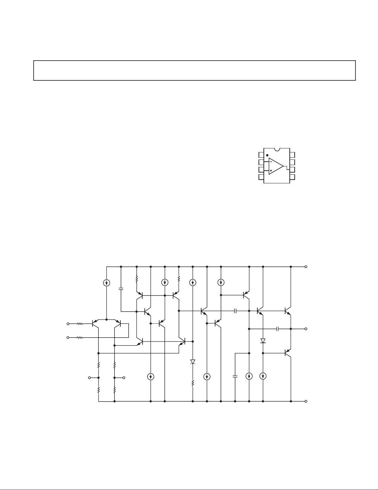
Figure 1. Simplied Schematic
REV. A
Information furnished by Analog Devices is believed to be accurate and
reliable. However, no responsibility is assumed by Analog Devices for its
use, nor for any infringements of patents or other rights of third parties that
may result from its use. No license is granted by implication or otherwise
under any patent or patent rights of Analog Devices.
V+
OUTPUT
V–
One Technology Way, P.O. Box 9106, Norwood, MA 02062-9106, U.S.A.
Tel: 781/329-4700 www.analog.com
Fax: 781/326-8703 © Analog Devices, Inc., 2002
Page 2

OP90
–SPECIFICATIONS
ELECTRICAL CHARACTERISTICS
(VS = ⴞ1.5 V to ⴞ15 V, TA = 25ⴗC, unless otherwise noted.)
OP90A/E OP90G
Parameter Symbol Conditions Min Typ Max Min Typ Max Unit
INPUT OFFSET VOLTAGE V
INPUT OFFSET CURRENT I
INPUT BIAS CURRENT I
OS
OS
B
LARGE-SIGNAL V
VOLTAGE GAIN A
VO
A
VO
A
VO
VCM = 0 V 0.4 3 0.4 5 nA
VCM = 0 V 4.0 15 4.0 25 nA
= ±15 V, VO = ±10 V
S
RL = 100 kΩ 700 1200 400 800 V/mV
RL= 10 kΩ 350 600 200 400 V/mV
RL = 2 kΩ 125 250 100 200 V/mV
50 150 125 450 µV
V+ = 5 V, V– = 0 V,
< 4 V
O
INPUT VOLTAGE RANGE
1
1 V < V
A
VO
A
VO
RL = 100 kΩ 200 400 100 250 V/mV
RL = 10 kΩ 100 180 70 140 V/mV
IVR V+ = 5 V, V– = 0 V 0/4 0/4 V
VS = ±15 V –15/13.5 –15/13.5 V
OUTPUT VOLTAGE SWING V
O
V
OH
V
OL
VS = ±15 V
R
= 10 kΩ±14 ± 14.2 ±14 ±14.2 V
L
= 2 kΩ±11 ± 12 ± 11 ± 12 V
R
L
V+ = 5 V, V– = 0 V
R
= 2 kΩ 4.0 4.2 4.0 4.2 V
L
V+ = 5 V, V– = 0 V
RL = 10 kΩ 100 500 100 500 µV
COMMON-MODE CMR V+ = 5 V, V– = 0 V,
REJECTION 0 V < VCM < 4 V 90 110 80 100 dB
CMR V
= ±15 V,
S
–15 V < VCM < 13.5 V 100 130 90 120 dB
POWER SUPPLY
REJECTION RATIO PSRR 1.0 5.6 3.2 10 µV/V
SLEW RATE SR VS = ±15 V 5 12 5 12 V/ms
SUPPLY CURRENT I
CAPACITIVE LOAD A
STABILITY
2
INPUT NOISE VOLTAGE e
I
SY
SY
n p-p
VS = ±1.5 V 9 15 9 15 µA
VS = ±15 V 14 20 14 20 µA
= 1
V
No Oscillations 250 650 250 650 pF
fO = 0.1 Hz to 10 Hz
VS = ±15 V 3 3 µV p-p
INPUT RESISTANCE
DIFFERENTIAL MODE R
IN
VS = ±15 V 30 30 MΩ
INPUT RESISTANCE
COMMON-MODE R
NOTES
1
Guaranteed by CMR test.
2
Guaranteed but not 100% tested.
Specifications subject to change without notice.
INCM
VS = ±15 V 20 20 GΩ
–2–
REV. A
Page 3

OP90
ELECTRICAL CHARACTERISTICS
(VS = ⴞ1.5 V to ⴞ15 V, –55ⴗC TA +125ⴗC, unless otherwise noted.)
Parameter Symbol Conditions Min Typ Max Unit
INPUT OFFSET VOLTAGE V
OS
80 400 µV
AVERAGE INPUT OFFSET
VOLTAGE DRIFT TCV
INPUT OFFSET CURRENT I
INPUT BIAS CURRENT I
OS
B
OS
V
= 0 V 1.5 5 nA
CM
V
= 0 V 4.0 20 nA
CM
0.3 2.5 µV/°C
LARGE-SIGNAL
VOLTAGE GAIN A
VO
A
VO
VS = ±15 V, VO = ±10 V
= 100 kΩ 225 400 V/mV
R
L
R
= 10 kΩ 125 240 V/mV
L
= 2 kΩ 50 110 V/mV
R
L
V+ = 5 V, V– = 0 V,
1 V < V
R
L
< 4 V
O
= 100 kΩ 100 200 V/mV
RL = 10 kΩ 50 110 V/mV
INPUT VOLTAGE RANGE
*
IVR V+ = 5 V, V– = 0 V 0/3.5 V
VS = ±15 V –15/13 5 V
OUTPUT VOLTAGE SWING V
O
V
OH
V
OL
VS = ±15 V
R
= 10 kΩ±13.5 ± 13.7 V
L
= 2 kΩ±10.5 ± 11.5 V
R
L
V+ = 5 V, V– = 0 V
R
= 2 kΩ 3.9 4.1 V
L
V+ = 5 V, V– = 0 V
RL = 10 kΩ 100 500 µV
COMMON-MODE
REJECTION CMR V+ = 5 V, V– = 0 V,
0 V < V
= ±15 V,
V
S
< 3.5 V 85 105 dB
CM
15 V < VCM < 13.5 V 95 115 dB
POWER SUPPLY
REJECTION RATIO PSRR 3.2 10 µV/V
SUPPLY CURRENT I
SY
VS = ±1.5 V 15 25 µA
VS = ±15 V 19 30 µA
NOTE
*Guaranteed by CMR test.
REV. A
–3–
Page 4

OP90
(VS = ⴞ1.5 V to ⴞ15 V, –25ⴗC TA +85ⴗC for OP90E/F, –40ⴗC TA +85ⴗC for
ELECTRICAL CHARACTERISTICS
Parameter Symbol Conditions Min Typ Max Min Typ Max Unit
INPUT OFFSET VOLTAGE V
AVERAGE INPUT OFFSET
VOLTAGE DRIFT TCV
INPUT OFFSET CURRENT I
INPUT BIAS CURRENT I
LARGE-SIGNAL A
VOLTAGE GAIN R
INPUT VOLTAGE RANGE* IVR V+ = 5 V, V– = 0 V 0/3.5 0/3.5 V
OUTPUT VOLTAGE SWING V
COMMON-MODE CMR V+ = 5 V, V– = 0 V,
REJECTION 0 V < V
POWER SUPPLY
REJECTION RATIO PSRR 10 5.6 5.6 17.8 µV/V
SUPPLY CURRENT I
NOTE
*Guaranteed by CMR test.
OS
OS
OS
B
VO
A
VO
O
V
OH
V
OL
SY
OP90G, unless otherwise noted.)
OP9OE OP9OG
70 270 180 675 µV
0.3 2 1.2 5 µV/°C
VCM = 0 V 0.8 3 1.3 7 nA
VCM = 0 V 4.0 15 4.0 25 nA
VS = ±15 V, VO = ±10 V
= 100 kΩ 500 800 300 600 V/mV
L
= 10 kΩ 250 400 150 250 V/mV
R
L
= 2 kΩ 100 200 75 125 V/mV
R
L
V+ = 5 V, V– = 0 V,
1 V < V
R
< 4 V
O
= 100 kΩ 150 280 80 160 V/mV
L
RL = 10 kΩ 75 140 40 90 V/mV
VS = ±15 V –15/13.5 –15/13.5 V
VS = ±15 V
= 10 kΩ±13.5 ± 14 ±13.5 ± 14 V
R
L
R
= 2 kΩ±10.5 ± 11.8 ± 10.5 ±11.8 V
L
V+ = 5 V, V– = 0 V
= 2 kΩ 3.9 4.1 3.9 4.1 V
R
L
V+ = 5 V, V– = 0 V
RL = 10 kΩ 100 500 100 500 µV
< 3.5 V 80 100 80 100 dB
CM
= ±15 V,
V
S
–15 V < VCM < 13.5 V 100 120 90 110 dB
VS = ±1.5 V 13 25 12 25 µA
VS = ±15 V 17 30 16 30 µA
–4–
REV. A
Page 5

OP90
WARNING!
ESD SENSITIVE DEVICE
ABSOLUTE MAXIMUM RATINGS
1
Supply Voltage . . . . . . . . . . . . . . . . . . . . . . . . . . . . . . . . ±18 V
Differential Input Voltage . . . . [(V–) – 20 V] to [(V+) + 20 V]
Common-Mode Input Voltage . . . . . . . . . . . . . . . . . . . . . . . .
. . . . . . . . . . . . . . . . . . . . . . . . [(V–) – 20 V] to [(V+) + 20 V]
Output Short-Circuit Duration . . . . . . . . . . . . . . . . Indefinite
Storage Temperature Range
Z Package . . . . . . . . . . . . . . . . . . . . . . . . . –65°C to +150°C
P Package . . . . . . . . . . . . . . . . . . . . . . . . . –65°C to +150°C
Operating Temperature Range
OP90A . . . . . . . . . . . . . . . . . . . . . . . . . . . –55°C to +125°C
OP90E . . . . . . . . . . . . . . . . . . . . . . . . . . . . –25°C to +85°C
OP90G . . . . . . . . . . . . . . . . . . . . . . . . . . . . –40°C to +85°C
Junction Temperature (T
) . . . . . . . . . . . . . –65°C to +150°C
J
Lead Temperature (Soldering 60 sec) . . . . . . . . . . . . . . 300°C
Package Type
2
JA
JC
Unit
8-Lead Hermetic DIP (Z) 148 16 °C/W
8-Lead Plastic DIP (P) 103 43 °C/W
8-Lead SO (S) 158 43 °C/W
NOTES
1
Absolute Maximum Ratings apply to packaged parts, unless otherwise noted.
2
is specified for worst-case mounting conditions; i.e., JA is specified for
JA
device in socket for CerDIP, and P-DIP; JA is specified for devices soldered to
printed circuit board for SO package.
ORDERING GUIDE
Package Options
T
= 25ⴗC Operating
A
V
Max CERDIP Plastic Temperature
OS
(mV) 8-Lead 8-Lead Range
150 OP90AZ/883* MIL
150 OP90EZ* IND
450 OP90GP XIND
450 OP90GS XIND
*Not for new design, obsolete April 2002.
CAUTION
ESD (electrostatic discharge) sensitive device. Electrostatic charges as high as 4000 V readily
accumulate on the human body and test equipment and can discharge without detection. Although
the OP90 features proprietary ESD protection circuitry, permanent damage may occur on devices
subjected to high-energy electrostatic discharges. Therefore, proper ESD precautions are
recommended to avoid performance degradation or loss of functionality.
REV. A
–5–
Page 6

OP90
–Typical Performance Characteristics
100
VS = ⴞ15V
80
60
40
20
INPUT OFFSET VOLTAGE – V
0
–75 –50 125
0 25 100
TEMPERATURE – C
7550–25
TPC 1. Input Offset Voltage
vs. Temperature
22
NO LOAD
20
18
16
14
VS = ⴞ15V
12
10
8
VS = ⴞ1.5V
SUPPLY CURRENT – A
6
4
2
–75 –50 125
0 25 100
TEMPERATURE – C
7550–25
TPC 4. Supply Current vs.
Temperature
1.6
VS = ⴞ15V
1.4
1.2
1.0
0.8
0.6
INPUT OFFSET CURRENT – nA
0.4
0.2
–75 –50 125
0 25 100
TEMPERATURE – C
7550–25
TPC 2. Input Offset Current
vs. Temperature
600
RL = 10k⍀
500
400
300
200
OPEN-LOOP GAIN – V/mV
100
0
030
10 15 25
SINGLE-SUPPLY VOLTAGE – V
TA = 25 C
TA = 85 C
TA = 125 C
205
TPC 5. Open-Loop Gain vs.
Single-Supply Voltage
4.2
4.0
3.8
3.6
3.4
INPUT BIAS CURRENT – nA
3.2
3.0
–75 –50 125
TEMPERATURE – C
TPC 3. Input Bias Current
vs. Temperature
140
120
100
GAIN
0
0.1 1 100k
OPEN-LOOP GAIN – dB
80
60
40
20
TPC 6. Open-Loop Gain and
Phase Shift vs. Frequency
VS = ⴞ15V
0 25 100
10 100 10k
FREQUENCY – Hz
7550–25
VS = ⴞ15V
T
R
1k
= 25ⴗC
A
= 100k⍀
L
0
45
90
135
180
PHASE SHIFT – DEG
60
40
20
0
CLOSED-LOOP GAIN – dB
–20
10 100k
1k
FREQUENCY – Hz
VS = ⴞ15V
= 25ⴗC
T
A
10k100
TPC 7. Closed-Loop Gain
vs. Frequency
6
V+ = 5V, V– = 0V
= 25ⴗC
T
A
5
4
3
2
OUTPUT VOLTAGE SWING – V
1
0
100 100k
1k
LOAD RESISTANCE – ⍀
10k
TPC 8. Output Voltage Swing
vs. Load Resistance
–6–
16
14
12
10
8
6
OUTPUT SWING – V
4
2
0
100 100k
POSITIVE
NEGATIVE
1k
LOAD RESISTANCE – ⍀
10k
T
= 25ⴗC
A
= ⴞ15V
V
S
TPC 9. Output Voltage Swing
vs. Load Resistance
REV. A
Page 7

OP90
120
TA = 25ⴗC
100
80
60
40
POWER SUPPLY REJECTION – dB
20
11k
NEGATIVE SUPPLY
POSITIVE SUPPLY
10 100
FREQUENCY – Hz
TPC 10. Power Supply Rejection
vs. Frequency
100
10
1
CURRENT NOISE DENSITY – pA/ 兹Hz
0.1
0.1 1k
110
FREQUENCY – Hz
VS = ⴞ15V
= 25ⴗC
T
A
100
TPC 13. Current Noise Density
vs. Frequency
140
120
100
80
60
COMMON-MODE REJECTION – dB
40
11k
TPC 11. Common-Mode Rejection
vs. Frequency
TA = 25ⴗC
VS = ⴞ15V
= +1
A
V
= 10k⍀
R
L
CL = 500pF
TPC 14. Small-Signal Transient
Response
10 100
FREQUENCY – Hz
VS = ⴞ15V
TA = 25ⴗC
1000
100
10
NOISE VOLTAGE DENSITY – nV/ 兹Hz
1
0.1 1k
110
FREQUENCY – Hz
VS = ⴞ15V
= 25ⴗC
T
A
100
TPC 12. Noise Voltage Density
vs. Frequency
TA = 25ⴗC
= ⴞ15V
V
S
= +1
A
V
= 10k⍀
R
L
C
= 500pF
L
TPC 15. Large-Signal Transient
Response
REV. A
+18V
2
7
OP90
3
6
4
–18V
Figure 2. Burn-In Circuit
APPLICATION INFORMATION
Battery-Powered Applications
The OP90 can be operated on a minimum supply voltage of 1.6 V,
or with dual supplies ±0.8 V, and draws only 14 pA of supply
current. In many battery-powered circuits, the OP90 can be
continuously operated for thousands of hours before requiring
battery replacement, reducing equipment down time and
operating cost.
High-performance portable equipment and instruments frequently
use lithium cells because of their long shelf-life, light weight, and
high-energy density relative to older primary cells. Most lithium
cells have a nominal output voltage of 3 V and are noted for a
flat discharge characteristic. The low-supply voltage requirement
of the OP90, combined with the flat discharge characteristic of
the lithium cell, indicates that the OP90 can be operated over
the entire useful life of the cell. Figure 1 shows the typical discharge characteristic of a 1Ah lithium cell powering an OP90
which, in turn, is driving full output swing into a 100 kΩ load.
–7–
Page 8

OP90
4
3
2
CELL VOLTAGE – V
1
LITHIUM SULPHUR DIOXIDE
0
0 2000 7000
1000 3000 60005000
4000
HOURS
Figure 3. Lithium Sulphur Dioxide Cell Discharge
Ω
Characteristic with OP90 and 100 k
Load
Input Voltage Protection
The OP90 uses a PNP input stage with protection resistors in
series with the inverting and noninverting inputs. The high
breakdown of the PNP transistors coupled with the protection
resistors provides a large amount of input protection, allowing
the inputs to be taken 20 V beyond either supply without damaging the amplifier.
Offset Nulling
The offset null circuit of Figure 4 provides 6 mV of offset adjustment range. A 100 kΩ resistor placed in a series with the wiper
of the offset null potentiometer, as shown in Figure 5, reduces
the offset adjustment range to 400 µV and is recommended for
applications requiring high null resolution. Offset nulling does not
affect TCV
performance.
OS
TEST CIRCUITS
V+
2
7
OP90
3
1
6
4
5
100k⍀
V–
Single-Supply Output Voltage Range
In single-supply operation, the OP90’s input and output ranges
include ground. This allows true “zero-in, zero-out” operation.
The output stage provides an active pull-down to around 0.8 V
above ground. Below this level, a load resistance of up to 1 MΩ
to ground is required to pull the output down to zero.
In the region from ground to 0.8 V, the OP90 has voltage gain
equal to the data sheet specification. Output current source
capatibility is maintained over the entire voltage range including ground.
APPLICATIONS
Battery-Powered Voltage Reference
The circuit of Figure 6 is a battery-powered voltage reference
that draws only 17 µA of supply current. At this level, two AA
cells can power this reference over 18 months. At an output voltage
of 1.23 V @ 25°C, drift of the reference is only at 5.5 µV/°C over
the industrial temperature range. Load regulation is 85 µV/mA
with line regulation at 120 µV/V.
Design of the reference is based on the bandgap technique.
Scaling of resistors R1 and R2 produces unequal currents in Q1
and Q2. The resulting V
mismatch creates a temperature
BE
proportional voltage across R3 which, in turn, produces a larger
temperature-proportional voltage across R4 and R5. This voltage appears at the output added to the V
of Q1, which has an
BE
opposite temperature coefficient. Adjusting the output to l.23 V
at 25°C produces minimum drift over temperature. Bandgap
references can have start-up problems. With no current in R1
and R2, the OP90 is beyond its positive input range limit and
has an undefined output state. Shorting Pin 5 (an offset adjust
pin) to ground, forces the output high under these conditions
and ensures reliable start-up without significantly degrading the
OP90’s offset drift.
V+
(2.5V TO 36V)
C1
1000pF
R1
240k⍀
R2
1.5M⍀
2
3
OP90
4
7
6
5
V
OUT
(1.23V @ 25ⴗC)
Figure 4. Offset Nulling Circuit
V+
2
7
OP90
3
1
6
4
5
100k⍀
100k⍀
V–
Figure 5. High Resolution Offset Nulling Circuit
–8–
20k⍀
OUTPUT
ADJUST
MAT-01AH
1
2
3
R3
68k⍀
R4
130k⍀
R5
7
6
5
Figure 6. Battery-Powered Voltage Reference
REV. A
Page 9

OP90
Single Op Amp Full-Wave Rectifier
Figure 7 shows a full-wave rectifier circuit that provides the
absolute value of input signals up to ±2.5 V even though operated
from a single 5 V supply. For negative inputs, the amplifier acts
as a unity-gain inverter. Positive signals force the op amp output
to ground. The 1N914 diode becomes reversed-biased and the
signal passes through R1 and R2 to the output. Since output
impedance is dependent on input polarity, load impedances
cause an asymmetric output. For constant load impedances, this
can be corrected by reducing R2. Varying or heavy loads can be
buffered by a second OP90. Figure 8 shows the output of the
full-wave rectifier with a 4 V
IN
HP5082-2800
R1
10k⍀
V
, 10 Hz input signal.
p-p
R2
10k⍀
+5V
2
7
6
4
R3
100k⍀
3
OP90FZ
1N914
V
OUT
Figure 7. Single Op Amp Full-Wave Rectifier
2-WIRE 4 mA TO 20 mA CURRENT TRANSMITTER
The current transmitter of Figure 9 provides an output of 4 mA
to 20 mA that is linearly proportional to the input voltage.
Linearity of the transmitter exceeds 0.004% and line rejection is
0.0005%/volt.
Biasing for the current transmitter is provided by the REF-02EZ.
The OP90EZ regulates the output current to satisfy the current
summation at the noninverting node:
VR
1
=+
R
6
I
OUT
5
IN
R
2
VR
55
R
1
For the values shown in Figure 9,
16
1004Ω
+
IVmA
=
OUT IN
giving a full-scale output of 20 mA with a 100 mV input.
Adjustment of R2 will provide an offset trim and adjustment of
R1 will provide a gain trim. These trims do not interact since
the noninverting input of the OP90 is at virtual ground. The
Schottky diode, D1, prevents input voltage spikes from pulling
the noninverting input more than 300 mV below the inverting
input. Without the diode, such spikes could cause phase reversal of
the OP90 and possible latch-up of the transmitter. Compliance of
this circuit is from 10 V to 40 V. The voltage reference output
can provide up to 2 mA for transducer excitation.
Figure 8. Output of Full-Wave Rectifier with 4 V
10 Hz Input
+5V
REFERENCE
2mA MAX
R1
1M⍀
R2
+
5k⍀
V
IN
–
D1
HP
50822800
Figure 9. 2-Wire 4 mA to 20mA Transmitter
p-p
,
2
4
2N1711
R6
100⍀
I
OUT
V+
(10V TO 40V)
R
L
2
3
R3
4.7k⍀
OP90EZ
R5
80k⍀
6
REF-02EZ
7
6
4
R4
100k⍀
16V
IN
I
OUT
+ 4mA
=
100⍀
REV. A
–9–
Page 10

OP90
Micropower Voltage-Controlled Oscillator
Two OP90s in combination with an inexpensive quad CMOS
switch comprise the precision VCO of Figure 10. This circuit
provides triangle and square wave outputs and draws only 50 µA
from a single 5 V supply. A1 acts as an integrator; S1 switches
the charging current symmetrically to yield positive and negative
ramps. The integrator is bounded by A2 which acts as a Schmitt
trigger with a precise hysteresis of 1.67 V, set by resistors R5,
R6, and R7, and associated CMOS switches. The resulting output
of A1 is a triangular wave with upper and lower levels of 3.33 V
and 1.67 V. The output of A2 is a square wave with almost
rail-to-rail swing. With the components shown, frequency of
operation is given by the equation:
fV V HzV
=
OUT CONTROL
× 10 /
()
but this is easily changed by varying C1. The circuit operates
well up to a few hundred hertz.
Micropower Single-Supply Instrumentation Amplifier
The simple instrumentation amplifier of Figure 11 provides over
110 dB of common-mode rejection and draws only 15 µA of
supply current. Feedback is to the trim pins rather than to the
inverting input. This enables a single amplifier to provide differential to single-ended conversion with excellent common-mode
rejection. Distortion of the instrumentation amplifier is that of a
differential pair, so the circuit is restricted to high gain applica-
C1
+5V
75nF
V
CONTROL
R1
200k⍀
R2
200k⍀
R3
100k⍀
1
2
IN/OUT
OUT/IN
2
3
R4
200k⍀
CD4066
S1
OP90EZ
A1
7
4
V
CONT
6
14
DD
13
tions. Nonlinearity is less than 0.1% for gains of 500 to 1000
over a 2.5 V output range. Resistors R3 and R4 set the voltage
gain and, with the values shown, yield a gain of 1000. Gain
tempco of the instrumentation amplifier is only 50 ppm/°C.
Offset voltage is under 150 µV with drift below 2 µV/°C. The
OP90’s input and output voltage ranges include the negative
rail which allows the instrumentation amplifier to provide true
“zero-in, zero-out” operation.
+5V
–IN
+IN
2
3
7
OP90EZ
1
4
R1
4.3M⍀
6
5
0.1F
R4
3.9M⍀
R3
1M⍀
R2
500k⍀
GAIN
ADJUST
V
OUT
Figure 11. Micropower Single-Supply Instrumentation
Amplifier
+5V
R5
+5V
200k⍀
2
7
+5V
TRIANGLE
OUT
R8
200k⍀
+5V
OP90EZ
A2
3
4
R6
200k⍀R7200k⍀
6
SQUARE
OUT
CONT
IN/OUT
OUT/IN
OUT/IN
IN/OUT
12
11
10
9
+5V
8
3
4
5
6
7
OUT/IN
IN/OUT
CONT
CONT
V
SS
S2
S3
S4
Figure 10. Micropower Voltage Controlled Oscillator
–10–
REV. A
Page 11

Single-Supply Current Monitor
R1
1⍀
R4
9.9k⍀
R2
100k⍀
R3
100k⍀
3
7
6
4
2
5
1
V+
R5
100⍀
I
TEST
V
OUT
= 100mV/mA (I
TEST
)
TO CIRCUIT
UNDER TEST
–
+
OP90EZ
Current monitoring essentially consists of amplifying the voltage
drop across a resistor placed in a series with the current to be
measured. The difficulty is that only small voltage drops can be
tolerated and with low precision op amps this greatly limits the
overall resolution. The single supply current monitor of Figure 12
has a resolution of 10 µA and is capable of monitoring 30 mA of
current. This range can be adjusted by changing the current
sense resistor R1. When measuring total system current, it may
be necessary to include the supply current of the current monitor, which bypasses the current sense resistor, in the final result.
This current can be measured and calibrated (together with the
residual offset) by adjustment of the offset trim potentiometer,
R2. This produces a deliberate offset that is temperature
dependent. However, the supply current of the OP90 is also
proportional to temperature and the two effects tend to track.
Current in R4 and R5, which also bypasses R1, can be accounted
for by a gain trim.
OP90
Figure 12. Single-Supply Current Monitor
REV. A
–11–
Page 12

OUTLINE DIMENSIONS
Dimensions shown in inches and (mm).
PIN 1
0.210
(5.33)
MAX
0.160 (4.06)
0.115 (2.93)
0.022 (0.558)
0.014 (0.356)
8-Lead PDIP Package
(N-8)
0.430 (10.92)
0.348 (8.84)
8
0.100 (2.54)
5
0.280 (7.11)
14
BSC
0.240 (6.10)
0.060 (1.52)
0.015 (0.38)
0.070 (1.77)
0.045 (1.15)
0.130
(3.30)
MIN
SEATING
PLANE
0.325 (8.25)
0.300 (7.62)
0.015 (0.381)
0.008 (0.204)
0.1574 (4.00)
0.1497 (3.80)
0.195 (4.95)
0.115 (2.93)
8-Lead Soic Package
0.1968 (5.00)
0.1890 (4.80)
85
0.2440 (6.20)
0.2284 (5.80)
41
(R-8)
0.005 (0.13)
PIN 1
0.200 (5.08)
MAX
0.200 (5.08)
0.125 (3.18)
8-Lead Hermetic Package
(Q-8)
0.055 (1.4)
MIN
0.100 (2.54) BSC
0.405 (10.29) MAX
0.023 (0.58)
0.014 (0.36)
MAX
85
1
0.310 (7.87)
0.220 (5.59)
4
0.070 (1.78)
0.030 (0.76)
0.060 (1.52)
0.015 (0.38)
SEATING
PLANE
0.150
(3.81)
MIN
0.320 (8.13)
0.290 (7.37)
15°
0°
C00321–0–1/02(A)
0.015 (0.38)
0.008 (0.20)
PIN 1
0.0098 (0.25)
0.0040 (0.10)
SEATING
PLANE
0.0500 (1.27)
BSC
0.0192 (0.49)
0.0138 (0.35)
0.102 (2.59)
0.094 (2.39)
0.0098 (0.25)
0.0075 (0.19)
0.0196 (0.50)
0.0099 (0.25)
8ⴗ
0ⴗ
0.0500 (1.27)
0.0160 (0.41)
ⴛ 45ⴗ
Revision History
Location Page
9/01—Data Sheet changed from REV. 0 to REV. A.
Edits to PIN CONNECTIONS . . . . . . . . . . . . . . . . . . . . . . . . . . . . . . . . . . . . . . . . . . . . . . . . . . . . . . . . . . . . . . . . . . . . . . . . . . . . . 1
Edits to ELECTRICAL CHARACTERISTICS . . . . . . . . . . . . . . . . . . . . . . . . . . . . . . . . . . . . . . . . . . . . . . . . . . . . . . . . . . . . 2, 3, 4
Edits to ORDERING INFORMATION . . . . . . . . . . . . . . . . . . . . . . . . . . . . . . . . . . . . . . . . . . . . . . . . . . . . . . . . . . . . . . . . . . . . . . 5
Edits to ABSOLUTE MAXIMUM RATINGS . . . . . . . . . . . . . . . . . . . . . . . . . . . . . . . . . . . . . . . . . . . . . . . . . . . . . . . . . . . . . . . . . 5
Edits to PACKAGE TYPE . . . . . . . . . . . . . . . . . . . . . . . . . . . . . . . . . . . . . . . . . . . . . . . . . . . . . . . . . . . . . . . . . . . . . . . . . . . . . . . . 5
DELETED OP90 DICE CHARACTERISTICS . . . . . . . . . . . . . . . . . . . . . . . . . . . . . . . . . . . . . . . . . . . . . . . . . . . . . . . . . . . . . . . 5
DELETED WAFER TEST LIMITS . . . . . . . . . . . . . . . . . . . . . . . . . . . . . . . . . . . . . . . . . . . . . . . . . . . . . . . . . . . . . . . . . . . . . . . . 5
PRINTED IN U.S.A.
–12–
 Loading...