

Page 1
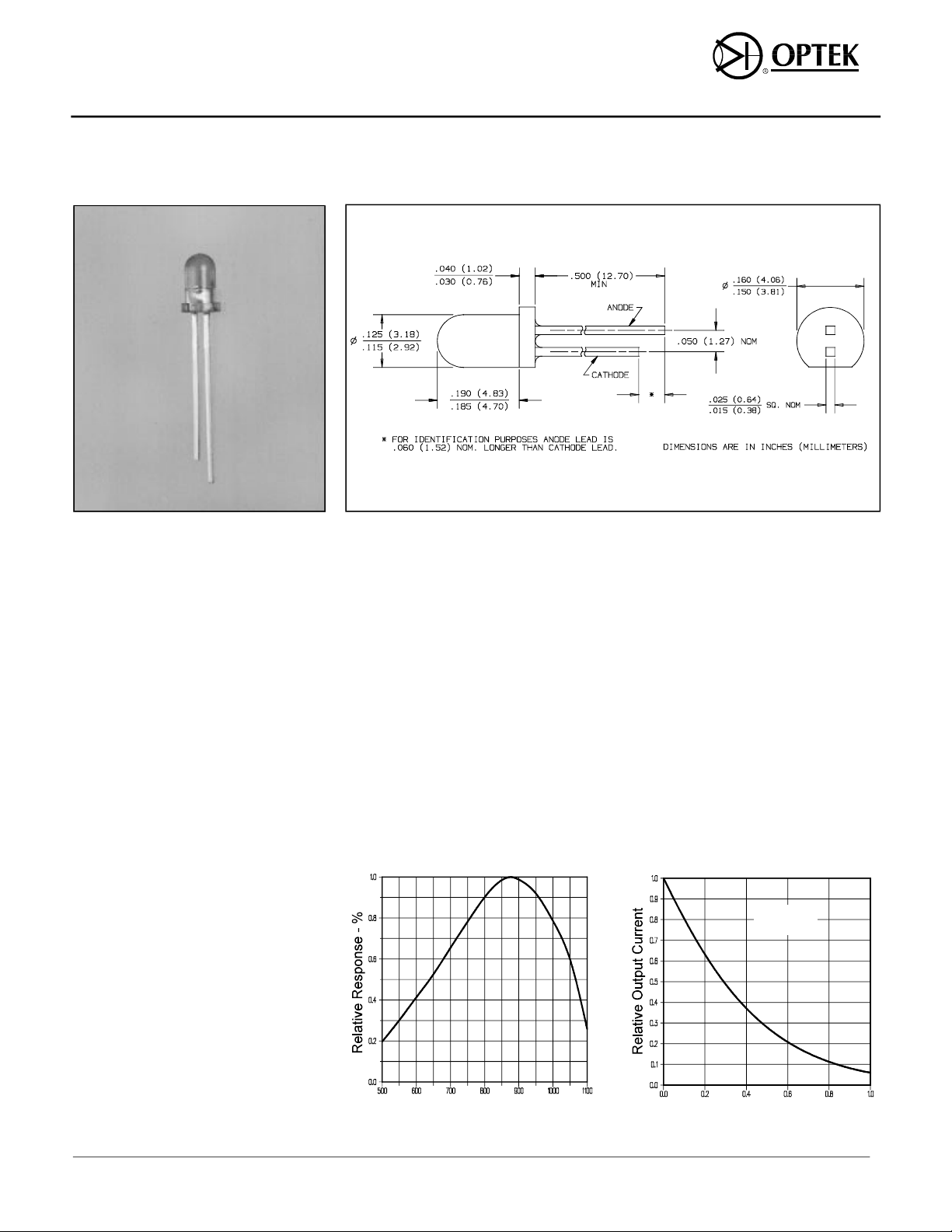
Prod uct Bul le tin OP905
June 1996
PIN Sili con Pho to di ode
Type OP905
Fea tures
• Narrow receiving angle
• Linear response vs. irradiance
• Fast switching time
• T-1 package style
• Small package ideal for space limited
applications
De scrip tion
The OP905 device consists of a PIN
silicon photodiode molded in a clear
epoxy package which allows spectral
response from visible to infrared light
wavelengths. The narrow receiving angle
provides excellent on-axis coupling.
These devices are 100% production
tested using infrared light for close
correlation with Optek’s GaAs and
GaAlAs emitters.
Ab so lute Maxi mum Rat ings (TA = 25o C un less oth er wise noted)
Re verse Break down Volt age. . . . . . . . . . . . . . . . . . . . . . . . . . . . . . . . . . . . . . . . . 60 V
Stor age and Op er at ing Tem pera ture Range. . . . . . . . . . . . . . . . . . -40o C to +100o C
Lead Sol der ing Tem pera ture [1/16 inch (1.6 mm) from case for 5 sec. with sol der ing
iron] . . . . . . . . . . . . . . . . . . . . . . . . . . . . . . . . . . . . . . . . . . . . . . . . . . . . . . . . 260o C
Power Dis si pa tion . . . . . . . . . . . . . . . . . . . . . . . . . . . . . . . . . . . . . . . . . . . . 100 mW
Notes:
(1) RMA flux is recommended. Duration can be extended to 10 sec. max. when flow soldering.
Max. 20 grams force may be applied to leads when soldering.
(2) Derate linearly 1.67 mW/o C above 25o C.
(3) Light source is an unfiltered GaAs LED with a peak emission wavelength of 935nm and a
radiometric intensity level which varies less than 10% over the entire lens surface of the
photodiode being tested.
(4) To calculate typical dark current in nA, use the formula ID = 10
ambient temperature in o C.
(0.042 TA-1.5)
where TA is
(1)
(2)
Typi cal Per form ance Curves
Relative Response vs.
Wavelength
Coupling Characteristics
OP905 and OP265
VR = 5 V
IF = 20 mA
λ - Wave length - nm
Op tek Tech nol ogy, Inc. 1215 W. Crosby Road Car roll ton, Texas 75006 (972) 323- 2200 Fax (972) 323- 2396
3-52
Dis tance Be tween Lens Tips - inches
Page 2
Type OP905
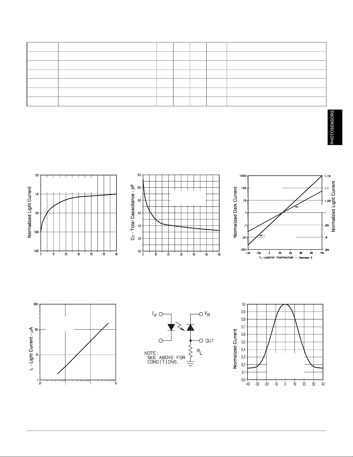
Elec tri cal Char ac ter is tics (TA = 25o C un less oth er wise noted)
SYM BOL PA RAME TER MIN TYP MAX UNITS TEST CON DI TIONS
I
I
V
(BR)
V
C
tr, t
Typi cal Per form ance Curves
Reverse Light Current 14 32 µA VR = 5 V, Ee = 0.50 mW/cm
L
Reverse Dark Current 1 60 nA VR = 30 V, Ee = 0
D
Reverse Breakdown Voltage 60 V IR = 100 µA
Forward Voltage 1.2 V IF = 1 mA
F
Total Capacitance 4 pF VR = 20 V, Ee = 0, f = 1.0 MHz
T
Rise Time, Fall Time 5 ns VR = 20 V, λ = 850 nm, RL = 50 Ω
f
2(3)
Normalized Light Current vs
Reverse Voltage
TA = 25o C
λ = 935 nm
Normalized to VR = 5 V
Total Capacitance vs
Reverse Voltage
TA = 25o C
Ee = 0 mW/cm
f = 1 MHz
2
Normalized Light and Dark
Current vs Ambient Temperature
VR = 5 V
λ = 935 nm
Normalized to
TA = 25o C
Dark Current
VR - Reverse Voltage - V VR - Reverse Voltage - V
Light Current vs. Irradiance Switching Time Test Circuit Light Current vs. Angular
VR = 5 V
TA = 25o C
λ = 935 nm
TA - Ambient Temperature - oC
Displacement
Light Current
Test Conditions:
λ = 935 nm
VR = 5 V
Distance Lens to
Lens = 1.5 inches
Ee - Irradiance - mW/cm
2
θ - Angular Displacement - Deg.
Op tek re serves the right to make changes at any time in or der to im prove de sign and to sup ply the best prod uct pos si ble.
Op tek Tech nol ogy, Inc. 1215 W. Crosby Road Car roll ton, Texas 75006 (972)323- 2200 Fax (972)323- 2396
3-53
 Loading...