

Page 1
Precision Picoampere Input Current
FEATURES
Low offset voltage: 75 μV maximum
Low offset voltage drift: 1.0 μV/°C maximum
Very low bias current
25°C: 150 pA maximum
−40°C to +85°C: 300 pA maximum
Very high open-loop gain: 2000 V/mV minimum
Low supply current (per amplifier): 625 μA maximum
Operates from ±2 V to ±20 V supplies
High common-mode rejection: 114 dB minimum
APPLICATIONS
Strain gage and bridge amplifiers
High stability thermocouple amplifiers
Instrumentation amplifiers
Photocurrent monitors
High gain linearity amplifiers
Long-term integrators/filters
Sample-and-hold amplifiers
Peak detectors
Logarithmic amplifiers
Battery-powered systems
GENERAL DESCRIPTION
The OP497 is a quad op amp with precision performance in
the space-saving, industry standard 16-lead SOlC package.
Its combination of exceptional precision with low power and
extremely low input bias current makes the quad OP497 useful
in a wide variety of applications.
Precision performance of the OP497 includes very low offset
(<50 µV) and low drift (<0.5 µV/°C). Open-loop gain exceeds
2000 V/mV ensuring high linearity in every application. Errors
due to common-mode signals are eliminated by its commonmode rejection of >120 dB. The OP497 has a power supply
rejection of >120 dB which minimizes offset voltage changes
experienced in battery-powered systems. The supply current
of the OP497 is <625 µA per amplifier, and it can operate with
supply voltages as low as ±2 V.
The OP497 uses a superbeta input stage with bias current
cancellation to maintain picoamp bias currents at all temperatures.
This is in contrast to FET input op amps whose bias currents
start in the picoamp range at 25°C but double for every 10°C
rise in temperature to reach the nanoamp range above 85°C.
The input bias current of the OP497 is <100 pA at 25°C.
Quad Operational Amplifier
OP497
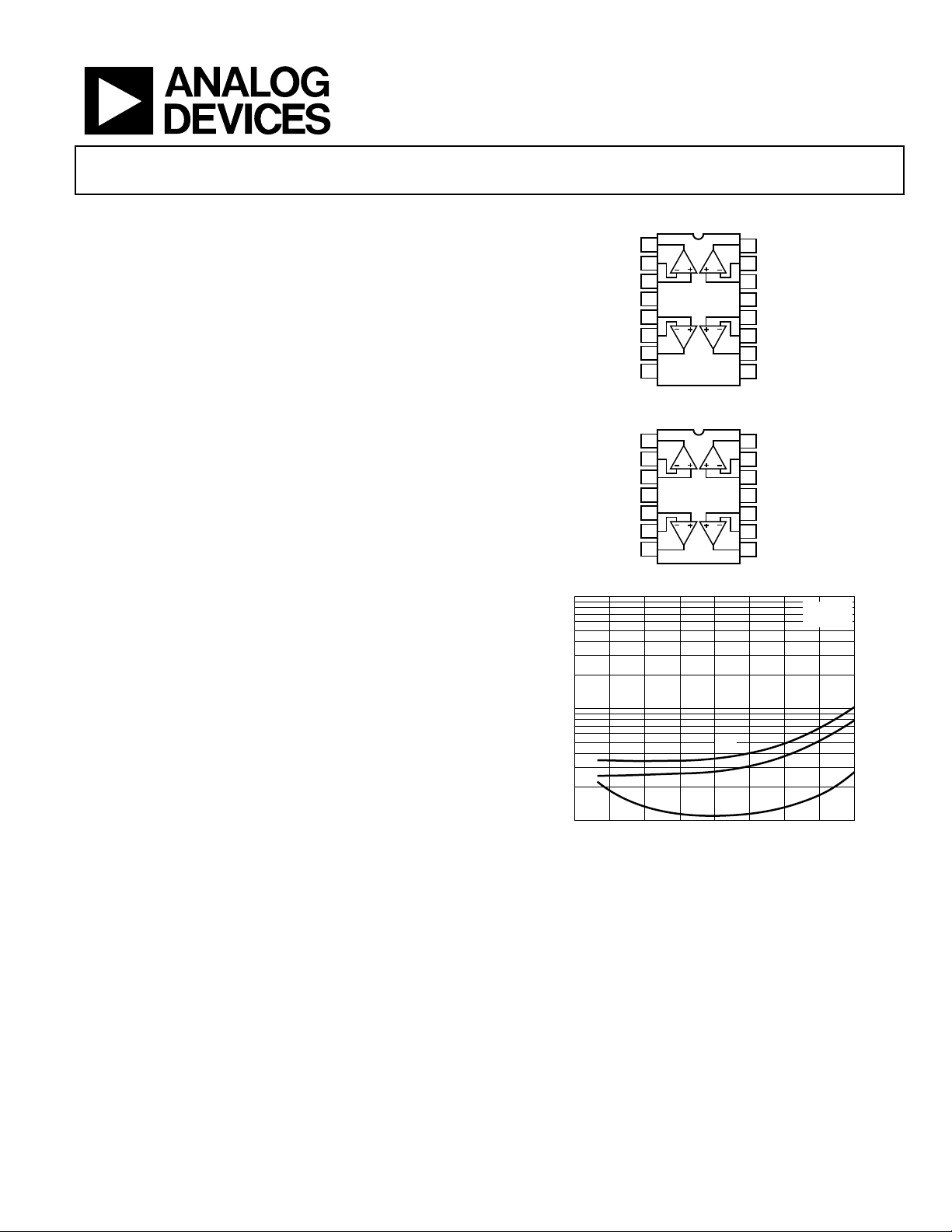
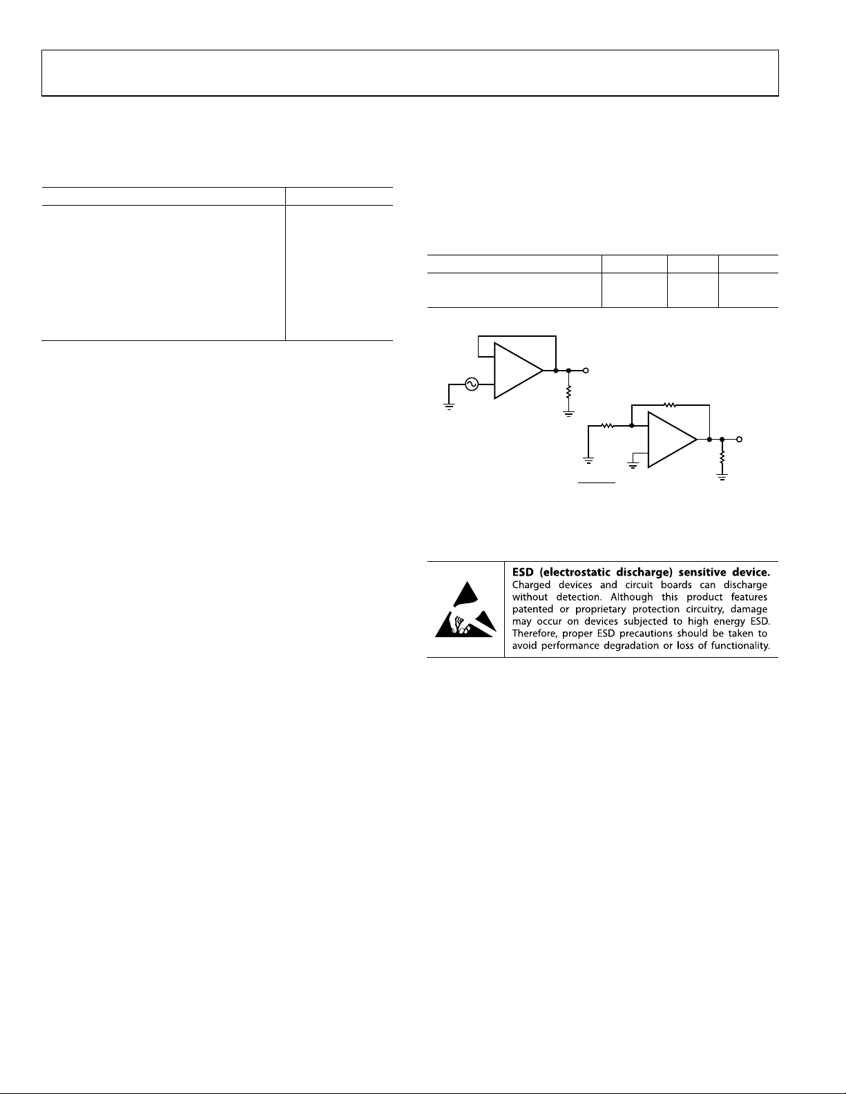
PIN CONNECTIONS
1
OUT A
2
–IN A
3
+IN A
4
V+
+IN B
–IN B
OUT B
NC
OP497
5
6
7
8
NC = NO CONNECT
Figure 1. 16-Lead Wide Body SOIC (RW-16)
1
OUT A
2
–IN A
3
+IN A
4
V+
+IN B
–IN B
OUT B
OP497
5
6
7
Figure 2. 14-Lead PDIP (N-14)
1k
100
INPUT CURRENT (pA)
10
–75 –50 –25 0 25 50 75 100 125
TEMPERATURE (°C)
Figure 3. Input Bias, Offset Current vs. Temperature
Combining precision, low power, and low bias current, the OP497
is ideal for a number of applications, including instrumentation
amplifiers, log amplifiers, photodiode preamplifiers, and longterm integrators. For a single device, see the OP97 data sheet,
and for a dual device, see the OP297 data sheet.
16
OUT D
15
–IN D
14
+IN D
13
V–
12
+IN C
11
–IN C
10
OUT C
9
NC
00309-001
14
OUT D
13
–IN D
12
+IN D
11
V–
10
+IN C
9
–IN C
8
OUT C
00309-002
VS = ±15V
= 0V
V
CM
–I
B
+I
B
I
OS
0309-003
Rev. E
Information furnished by Analog Devices is believed to be accurate and reliable. However, no
responsibility is assumed by Analog Devices for its use, nor for any infringements of patents or other
rights of third parties that may result from its use. Specifications subject to change without notice. No
license is granted by implication or otherwise under any patent or patent rights of Analog Devices.
Trademarks and registered trademarks are the property of their respective owners.
One Technology Way, P.O. Box 9106, Norwood, MA 02062-9106, U.S.A.
Tel: 781.329.4700 www.analog.com
Fax: 781.461.3113 ©1991–2009 Analog Devices, Inc. All rights reserved.
Page 2

OP497
TABLE OF CONTENTS
Features .............................................................................................. 1
Applications ....................................................................................... 1
General Description ......................................................................... 1
Pin Connections ............................................................................... 1
Revision History ............................................................................... 2
Specifications ..................................................................................... 3
Absolute Maximum Ratings ............................................................ 4
Thermal Resistance ...................................................................... 4
ESD Caution .................................................................................. 4
Typical Performance Characteristics ............................................. 5
Applications Information .............................................................. 10
REVISION HISTORY
2/09—Rev. D to Rev. E
Deleted 14-Lead CERDIP ............................................. Throughout
Changes to Features Section and General Description
Section ................................................................................................ 1
Delete Military Processed Devices Text, SMD Part Number,
ADI Part Number Table, and Dice Characteristics Figure ......... 3
Changes to Table 1 ............................................................................ 3
Changes to Absolute Maximum Ratings Section ......................... 4
Changes to Figure 12 ........................................................................ 6
Changes to Figure 18 and Figure 19 ............................................... 7
Changes to Figure 26 and Figure 28 ............................................... 8
Deleted OP497 Spice Macro-Model Section ............................... 10
Changes to Applications Information Section ............................ 10
Moved Figure 33 ............................................................................. 10
Deleted Table I. OP497 SPICE Net-List....................................... 11
Changes to Open-Loop Gain Linearity Section and
Figure 35 .......................................................................................... 11
Changes to Figure 40 ...................................................................... 13
Updated Outline Dimensions ....................................................... 14
Changes to Ordering Guide .......................................................... 15
AC Performance ......................................................................... 10
Guarding And Shielding ........................................................... 11
Open-Loop Gain Linearity ....................................................... 11
Applications Circuit ....................................................................... 12
Precision Absolute Value Amplifier ......................................... 12
Precision Current Pump ............................................................ 12
Precision Positive Peak Detector .............................................. 12
Simple Bridge Conditioning Amplifier ................................... 12
Nonlinear Circuits ...................................................................... 13
Outline Dimensions ....................................................................... 14
Ordering Guide .......................................................................... 15
11/01—Rev. C to Rev. D
Edits to Pin Connection Headings .................................................. 1
Deleted Wafer Test Limits ................................................................ 3
Edits to Absolute Maximum Ratings .............................................. 5
Edits to Outline Dimensions ......................................................... 16
Edits to Ordering Guide ................................................................ 17
Rev. E | Page 2 of 16
Page 3

OP497
SPECIFICATIONS
TA = 25°C, VS = ±15 V, unless otherwise noted.
Table 1.
F Grade G Grade
Parameter Symbol Condition Min Typ Max Min Typ Max Unit
INPUT CHARACTERISTICS
Offset Voltage VOS 40 75 80 150 μV
−40°C ≤ +85°C 70 150 120 250 μV
Average Input Offset Voltage Drift TCVOS T
Long-Term Input Offset Voltage
0.1 0.1 μV/Month
Stability
Input Bias Current IB V
−40° ≤ TA ≤ +85°C 60 200 80 300 pA
Average Input Bias Current Drift TCIB −40° ≤ TA ≤ +85°C 0.3 0.3 pA/°C
Input Offset Current IOS V
−40° ≤ TA ≤ +85°C 50 200 80 300 pA
Average Input Offset Current Drift TCIOS 0.3 0.4 pA/°C
Input Voltage Range1 IVR ±13 ±14 ±13 ±14 V
T
Common-Mode Rejection CMR VCM = ±13 V 114 135 114 135 dB
T
Large Signal Voltage Gain AVO V
−40° ≤ TA ≤ +85°C 800 2000 800 2000 V/mV
Input Resistance Differential Mode RIN 30 30 MΩ
Input Resistance Common Mode R
500 500 GΩ
INCM
Input Capacitance CIN 3 3 pF
OUTPUT CHARACTERISTICS
Output Voltage Swing V
O
R
R
Short Circuit ISC ±25 ±25 mA
POWER SUPPLY
Power Supply Rejection Ratio PSRR VS = ±2 V to ±20 V 114 135 114 135 dB
V
Supply Current (per Amplifier) ISY No load 525 625 525 625 μA
T
Supply Voltage Range VS Operating range ±2 ±20 ±2 ±20 V
T
DYNAMIC PERFORMANCE
Slew Rate SR 0.05 0.15 0.05 0.15 V/μs
Gain Bandwidth Product GBW 500 500 kHz
Channel Separation CS VO = 20 V p-p, fO = 10 Hz 150 150 dB
NOISE PERFORMANCE
Voltage Noise en p-p 0.1 Hz to 10 Hz 0.3 0.3 μV/p-p
Voltage Noise Density en e
e
Current Noise Density in in = 10 Hz 20 20 fA/√Hz
1
Guaranteed by CMR test.
− T
MIN
CM
CM
MIN
MIN
O
0.4 1.0 0.6 1.5 μV/°C
MAX
= 0 V 40 150 60 200 pA
= 0 V 30 150 50 200 pA
− T
±13 ±13.5 ±13 ±13.5 V
MAX
− T
108 120 108 120 dB
MAX
= ±10 V, RL = 2 kΩ 1500 4000 1200 4000 V/mV
RL = 2 kΩ ±13 ±13.7 ±13 ±13.7 V
= 10 kΩ, T
L
= 10 kΩ ±13 ±13.5 ±13 ±13.5 V
L
= ±2.5 V to ±20 V, T
S
− T
MIN
− T
MIN
= 10 Hz 17 17 nV/√Hz
n
= 1 kHz 15 15 nV/√Hz
n
− T
MIN
580 750 580 750 μA
MAX
±2.5 ±20 ±2.5 ±20 V
MAX
±13 ±14 ±13 ±14 V
MAX
− T
MIN
108 120 108 120 dB
MAX
Rev. E | Page 3 of 16
Page 4
OP497
ABSOLUTE MAXIMUM RATINGS
Absolute maximum ratings apply to packaged parts.
Table 2.
Parameter Rating
Supply Voltage ±20 V
Input Voltage1 20 V
Differential Input Voltage1 40 V
Output Short-Circuit Duration Indefinite
Storage Temperature Range −65°C to +150°C
Operating Temperature Range −40°C to +85°C
Junction Temperature Range −65°C to +150°C
Lead Temperature (Soldering, 60 sec) 300°C
1
For supply voltages less than ±20 V, the absolute maximum input voltage is
equal to the supply voltage.
Stresses above those listed under Absolute Maximum Ratings
may cause permanent damage to the device. This is a stress
rating only; functional operation of the device at these or any
other conditions above those indicated in the operational
section of this specification is not implied. Exposure to absolute
maximum rating conditions for extended periods may affect
device reliability.
THERMAL RESISTANCE
θJA is specified for the worst-case mounting conditions, that is,
is specified for a device in socket for the PDIP package, and
θ
JA
θ
is specified for a device soldered to the printed circuit board
JA
(PCB) for the SOIC package.
Table 3.
Package Type θJA θ
14-Lead PDIP (N-14) 76 33 °C/W
16-Lead SOIC (RW-16) 92 23 °C/W
–
1/4
OP497
+
CHANNEL SEPARATI ON = 20 log
Figure 4. Channel Separation Test Circuit
V1 20V p-p @ 10Hz
2kΩ
50Ω
V
1
()
V2/10,000
Unit
JC
50kΩ
–
1/4
OP497
+
V
2
00309-004
ESD CAUTION
Rev. E | Page 4 of 16
Page 5
OP497
TYPICAL PERFORMANCE CHARACTERISTICS
TA = 25°C, VS = ±15 V, unless otherwise noted.
50
40
30
20
PERCENTAGE OF UNITS
10
0
–100 –80 –60 –40 –20 0 20 40 60 80 100
INPUT OFFSET VOLTAGE (µV)
TA = 25°C
V
V
Figure 5. Typical Distribution of Input Offset Voltage
50
40
30
20
PERCENTAGE OF UNI T S
10
TA = 25°C
V
V
= ±15V
S
= 0V
CM
= ±15V
S
= 0V
CM
50
40
30
20
PERCENTAGE OF UNITS
10
0
0.1
0
00309-006
TCVOS (µV/°C)
Figure 8. Typical Distribution of TCV
OS
VS = ±15V
V
= 0V
CM
0.70.60.50.40.30.2
0.8
0309-009
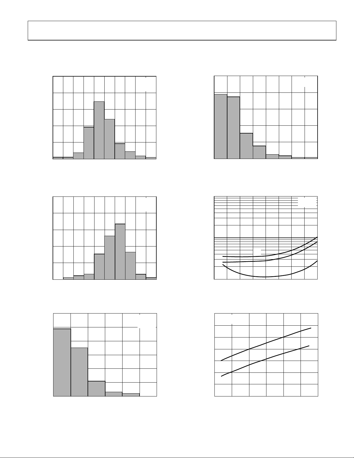
1k
100
–I
INPUT CURRENT (p A)
B
+I
VS = ±15V
V
= 0V
CM
B
0
–100 –80 –60 –40 –20 0 20 40 60 80 100
INPUT BIAS CURRENT (pA)
Figure 6. Typical Distribution of Input Bias Current
60
50
40
30
20
PERCENTAGE OF UNI T S
10
0
10
0
INPUT OFFSET CURRENT ( pA)
TA = 25°C
V
V
50403020
Figure 7. Typical Distribution of Input Offset Current
= ±15V
S
= 0V
CM
0309-007
60
0309-008
Rev. E | Page 5 of 16
I
10
–75 –50 –25 0 25 50 75 100 125
TEMPERATURE (°C)
OS
Figure 9. Input Bias, Offset Current vs. Temperature
70
TA = 25°C
V
= ±15V
S
60
50
40
30
20
INPUT BIAS CURRENT (pA)
10
0
–15
–10
COMMON-MODE VOLTAGE ( V)
1050–5
Figure 10. Input Bias Current vs. Common-Mode Voltage
00309-010
–I
B
+I
B
15
0309-011
Page 6

OP497
±3
T
A
V
S
V
CM
= 25°C
= ±15V
= 0V
1k
TA = 25°C
V
S
= ±2V TO ±20V
Hz)
±2
±1
DEVIATION FROM FINAL VALUE (µV)
0
0
TIME AFTER POWE R AP P LIED (Mi n utes)
Figure 11. Input Offset Voltage Warm-Up Drift
10k
BALANCED OR UNBALANCED
V
= ±15V
S
V
= 0V
CM
1k
100
EFFECTIVE OFFSET VOLTAGE (µV)
TA = 25°C
100
CURRENT NOISE
VOLTAGE NOISE
10
VOLTAGE NOISE DENSITY (nV/ Hz)
1
432
51
0309-012
1 10 100 1k
FREQUENCY (Hz)
CURRENT NOISE DE NS ITY (fA/
00309-015
Figure 14. Voltage Noise Density vs. Frequency
10
TA = 25°C
V
= ±2V TO ±20V
S
1
10Hz
1kHz
0.1
TOTAL NOISE DENSITY (µV/ Hz)
10
10 100 1k 10k 100k 1M 10M
SOURCE RESISTANCE (Ω)
Figure 12. Effective Offset Voltage vs. Source Resistance
100
BALANCED OR UNBALANCED
V
= ±15V
S
V
= 0V
CM
10
1
EFFECTIVE OFFSET VOLTAGE (µV/°C)
0.1
100 1k 10k 100k 1M 10M 100M
SOURCE RESISTANCE (Ω)
Figure 13. Effective TCVOS vs. Source Resistance
0.01
0309-013
100 1k 10k 100k 1M 10M
SOURCE RESIST ANCE (Ω)
0309-016
Figure 15. Total Noise Density vs. Source Resistance
1s5mV
100
90
10
0%
NOISE VO LTAGE ( 100mV /DIV)
0309-014
0246810
TIME (Seconds)
VS = ±15V
TA = 25°C
00309-017
Figure 16. 0.1 Hz to 10 Hz Noise Voltage
Rev. E | Page 6 of 16
Page 7

OP497
100
80
GAIN
60
PHASE
40
20
0
OPEN-LOOP GAIN (dB)
–20
–40
100
1k
FREQUENCY (Hz)
VS = ±15V
C
R
T
1M100k10k
= 30pF
L
= 1MΩ
L
= 25°C
A
10M
90
135
180
225
PHASE (Degrees)
0309-018
Figure 17. Open-Loop Gain and Phase vs. Frequency
10k
TA = 25°C
TA = 125°C
1k
160
140
120
100
80
60
40
COMMON-MODE REJECTION (dB)
20
0
101
FREQUENCY (Hz)
Figure 20. Common-Mode Rejection vs. Frequency
160
140
120
100
80
–PSR
+PSR
VS = ±15V
= 25°C
T
A
100k10k1k100
VS = ±15V
= 25°C
T
A
1M
0309-021
OPEN-LOOP GAIN (V/mV)
VS = ±15V
V
= ±10V
O
100
11
LOAD RESISTANCE (kΩ)
020
0309-019
Figure 18. Open-Loop Gain vs. Load Resistance
RL = 2kΩ
V
= ±15V
S
V
= ±10V
CN
TA = 125°C
TA = 25°C
DIFFERENTIAL I NPUT VOLTAGE (10µV/ DI V )
–15 –10 –5 0 5 10 15
OUTPUT VOLTAGE (V)
0309-020
Figure 19. Open-Loop Gain Linearity
60
40
POWER SUPP LY REJECTION (dB)
20
0
FREQUENCY (Hz)
Figure 21. Power Supply Rejection vs. Frequency
35
30
25
20
15
10
OUTPUT SWING (V p-p)
5
0
100
1k
FREQUENCY (Hz)
Figure 22. Maximum Output Swing vs. Frequency
10k
VS = ±15V
= 25°C
T
A
A
= +1
VCL
1% THD
= 10kΩ
R
L
1M101 100k10k1k100
0309-022
100k
0309-023
Rev. E | Page 7 of 16
Page 8

OP497
V
V
+
–0.5
–1.0
–1.5
S
T
A
= 25°C
700
600
500
NO LOAD
125°C
25°C
1.5
1.0
(REFERRED TO SUPPLY VOLTAGES)
INPUT COMMON-MODE VOLTAGE (V)
0.5
–V
S
0±5±10±15±
SUPPLY VOLTAGE (V)
Figure 23. Input Common-Mode Voltage Range vs. Supply Voltage
35
VS = ±15V
T
= 25°C
A
A
= +1
30
VCL
1% THD
f
= 1kHz
O
25
20
15
10
OUTPUT SWING (V p-p)
5
0
10
100
LOAD RESIST ANCE (Ω)
1k
10k
Figure 24. Maximum Output Swing vs. Load Resistance
+
S
–0.5
–1.0
–1.5
1.5
1.0
OUTPUT VOLTAGE SWING (V)
(REFERRED TO SUPPLY VOLTAGES)
0.5
–V
S
0±5±10±15±20
SUPPLY VOLTAGE (V)
TA = 25°C
R
= 10kΩ
L
Figure 25. Output Voltage Swing vs. Supply Voltage
20
0309-024
0309-025
0309-026
400
300
SUPPLY CURRENT (PER AMPLIFIER) (µA)
200
0 ±5 ±10 ±15 ±20
SUPPLY VOLTAGE (V)
Figure 26. Supply Current (per Amplifier) vs. Supply Voltage
1k
VS = ±15V
T
= 25°C
A
100
10
1
IMPEDANCE (Ω)
0.001
0.1
0.01
1
10
FREQUENCY (Hz)
AV = +1
10k1k100
100k
Figure 27. Closed-Loop Output Impedance vs. Frequency
35
30
25
20
15
VS = ±15V
OUTPUT SHORTED
TO GROUND
–15
–20
–25
SHORT-CIRCUI T CURRENT (mA)
–30
–35
0
TA = 125°C
TA = 25°C
1
TIME FROM OUTPUT SHORT (Minutes)
TA = 25°C
TA = 125°C
2
3
Figure 28. Short-Circuit Current vs. Time at Various Temperatures
0309-027
00309-028
4
0309-029
Rev. E | Page 8 of 16
Page 9

OP497
70
VS = ±15V
T
= 25°C
A
A
= +1
60
VCL
V
= 100mV p-p
OUT
50
40
30
OVERSHOOT (%)
20
10
0
10
100
LOAD CAPACITANCE ( pF)
1k
Figure 29. Small-Signal Overshoot vs. Load Capacitance
10k
0309-030
Rev. E | Page 9 of 16
Page 10

OP497
V
APPLICATIONS INFORMATION
Extremely low bias current makes the OP497 attractive for use
in sample-and-hold amplifiers, peak detectors, and log amplifiers
that must operate over a wide temperature range. Balancing
input resistances is not necessary with the OP497. High source
resistance, even when unbalanced, only minimally degrades the
offset voltage and TCV
.
OS
The input pins of the OP497 are protected against large differential
voltage by back-to-back diodes and current-limiting resistors.
Common-mode voltages at the inputs are not restricted and
may vary over the full range of the supply voltages used.
The OP497 requires very little operating headroom about the
supply rails and is specified for operation with supplies as low as
±2 V. Typically, the common-mode range extends to within 1 V
of either rail. When using a 10 kΩ load, the output typically
swings to within 1 V of the rails.
AC PERFORMANCE
The ac characteristics of the OP497 are highly stable over its full
operating temperature range. Figure 30 shows the unity-gain
small signal response. Extremely tolerant of capacitive loading
on the output, the OP497 displays excellent response even with
1000 pF loads (see Figure 31).
100
90
100
90
10
0%
20mV 5µs
Figure 31. Small Signal Transient Response (C
100
90
10
0%
2V 50µs
Figure 32. Large Signal Transient Response (A
= 1000 pF, A
LOAD
VCL
= +1)
0309-033
VCL
00309-034
= +1)
10
0%
20mV 5µs
Figure 30. Small Signal Transient Response (C
2.5kΩ
–IN
2.5kΩ
+IN
00309-032
= 100 pF, A
LOAD
VCL
= +1)
Figure 33. Simplified Schematic Showing One Amplifier
Rev. E | Page 10 of 16
+
V
OUT
V–
00309-031
Page 11

OP497
R
GUARDING AND SHIELDING
To maintain the extremely high input impedances of the OP497,
care must be taken in circuit board layout and manufacturing.
Board surfaces must be kept scrupulously clean and free of
moisture. Conformal coating is recommended to provide a
humidity barrier. Even a clean PCB can have 100 pA of leakage
currents between adjacent traces; therefore, use guard rings
around the inputs. Guard traces are operated at a voltage close
to that on the inputs, as shown in Figure 34, so that leakage
currents become minimal. In noninverting applications, connect
the guard ring to the common-mode voltage at the inverting
input. In inverting applications, both inputs remain at ground;
therefore, the guard trace should be grounded. Place guard
traces on both sides of the circuit board.
UNITY- GAIN F O LLOW E
NONINVERTI NG AMPLIFIER
OPEN-LOOP GAIN LINEARITY
The OP497 has both an extremely high gain of 2000 V/mV
typical and constant gain linearity. This enhances the precision
of the OP497 and provides for very high accuracy in high
closed-loop gain applications. Figure 35 illustrates the typical
open-loop gain linearity of the OP497.
RL = 10kΩ
V
= ±15V
S
V
= 0V
CM
TA = 125°C
TA = 25°C
INVERTING AMPLIFIER
–
1/4
OP497
+
–
1/4
OP497
+
–
1/4
OP497
+
PDIP
BOTTOM V IEW
8
B
Figure 34. Guard Ring Layout and Connections
DIFFERENTIAL I NPUT VOLTAGE (10µV/ DI V )
–15 –10 –5 0 5 10 15
OUTPUT VOLTAGE (V)
0309-036
Figure 35. Open-Loop Gain Linearity
1
A
00309-035
Rev. E | Page 11 of 16
Page 12

OP497
V
V
V
APPLICATIONS CIRCUIT
PRECISION ABSOLUTE VALUE AMPLIFIER
The circuit in Figure 36 is a precision absolute value amplifier
with an input impedance of 30 M. The high gain and low
TCV
of the OP497 ensure accurate operation with microvolt
OS
input signals. In this circuit, the input always appears as a commonmode signal to the op amps. The CMR of the OP497 exceeds
120 dB, yielding an error of less than 2 ppm.
+15
C2
0.1µF
C1
2
1/4
OP497
3
IN
30pF
8
1
C3
4
0.1µF
1kΩ
D1
1N4148
D2
1N4148
R1
R2
2kΩ
6
OP497
5
R3
1kΩ
1/4
7
0V < V
OUT
< 10V
PRECISION POSITIVE PEAK DETECTOR
In Figure 38, the CH must be of polystyrene, Teflon®, or
polyethylene to minimize dielectric absorption and leakage.
The droop rate is determined by the size of C
current of the OP497.
1kΩ
2
1/4
OP497
1kΩ
V
3
IN
Figure 38. Precision Positive Peak Detector
1
RESET
1N4148
C
H
1kΩ
2N930
1kΩ
+
6
OP497
5
1/4
and the bias
H
+15V
0.1µF
+
8
7
4
0.1µF
+
–15V
V
OUT
00309-039
–15V
00309-037
Figure 36. Precision Absolute Value Amplifier
PRECISION CURRENT PUMP
Maximum output current of the precision current pump shown
in Figure 37 is ±10 mA. Voltage compliance is ±10 V with ±15 V
supplies. Output impedance of the current transmitter exceeds
3 M with linearity better than 16 bits.
R3
R1
10kΩ
–
R2
V
IN
10kΩ
+
V
V
IN
===
R5
IN
100Ω
I
OUT
Figure 37. Precision Current Pump
2
3
R4
10kΩ
10mA/V
10kΩ
1/4
OP497
7
1
+15V
8
1/4
OP497
4
–15V
R5
10kΩ
I
OUT
±10mA
5
6
0309-038
SIMPLE BRIDGE CONDITIONING AMPLIFIER
Figure 39 shows a simple bridge conditioning amplifier using
the OP497. The transfer function is
OUT
⎛
⎜
=
VV
REF
⎜
⎝
⎞
R
R
F
⎟
⎟
Δ+
R
RR
⎠
The REF43 provides an accurate and stable reference voltage for
the bridge. To maintain the highest circuit accuracy, R
should
F
be 0.1% or better with a low temperature coefficient.
+5
2
REF43
4
V
REF
2.5V
6
R
R
6
OP497
5
1/4
R
R + ΔR
+5V
8
7
4
–5V
V
2
OP497
3
OUT
R
F
1/4
1
V
OUT
R
ΔR
= V
()
REF
R + ΔRR
F
00309-040
Figure 39. Simple Bridge Conditioning Amplifier Using the OP497
Rev. E | Page 12 of 16
Page 13

OP497
V
()(
V
NONLINEAR CIRCUITS
Due to its low input bias currents, the OP497 is an ideal log
amplifier in nonlinear circuits, such as the squaring amplifier
and square root amplifier circuits shown in Figure 40 and
Figure 41. Using the squaring amplifier circuit in Figure 40
as an example, the analysis begins by writing a voltage loop
equation across Transistors Q1, Q2, Q3, and Q4.
⎞
+
A2
1/4
–15V
T4
I
REF
R4
50kΩ
InV
R2
33kΩ
⎛
I
REF
⎟
⎜
⎟
⎜
I
S4
⎠
⎝
7
V
OUT
14
13
Q4
12
⎞
⎞
T1
⎟
⎜
I
S1
⎠
⎝
⎞
⎛
I
IN
⎟
⎜
InV
⎛
I
IN
⎟
⎜
InV
+
T2
⎟
⎜
I
S2
⎠
⎝
⎛
I
O
⎟
⎜
=
IInV
T3
⎟
⎜
I
S3
⎠
⎝
All the transistors in the MAT04 are precisely matched and at
the same temperature; therefore, the I
and VT terms cancel,
S
giving
2InI
= InIO + InI
IN
= In (IO × I
REF
REF
)
Exponentiating both sides of the thick equation lead to
2
()
I
IN
=
I
O
I
REF
Op amp A2 forms a current-to-voltage converter which results
in V
= R2 × IO. Substituting (VIN/R1) for IIN and the previous
OUT
=
yields
O
⎛
R2
⎜
⎜
I
REF
⎝
⎞
⎟
⎟
⎠
2
V
⎞
⎛
IN
⎟
⎜
R1
⎠
⎝
equation for I
V
OUT
C2
100pF
6
OP497
I
O
1
2
Q1
6
3
Q2
V+
R1
I
IN
133kΩ
IN
2
OP497
3
C1
A1
100pF
8
1/4
1
4
V–
Figure 40. Squaring Amplifier
5
7
5
MAT04
8
9
Q3
10
R3
50kΩ
00309-041
A similar analysis made for the square root amplifier circuit in
Figure 41 leads to its transfer function
)
IV
R2V
=
OUT
In these circuits, I
REF
REFIN
R1
is a function of the negative power supply. To
maintain accuracy, the negative supply should be well regulated.
For applications where very high accuracy is required, a voltage
reference can be used to set I
. An important consideration for
REF
the squaring circuit is that a sufficiently large input voltage can
force the output beyond the operating range of the output op
amp. Resistor R4 can be changed to scale I
, or R1 and R2 can
REF
be varied to keep the output voltage within the usable range.
R2
33kΩ
C2
100pF
6
1/4
7
V
I
O
OP497
5
1
Q1
I
IN
C1
100pF
R1
33kΩ
IN
2
OP497
3
1/4
V+
8
1
R5
4
V–
2kΩ
MAT04
2
3
7
8
6
Q3Q2
5
10
13
9
R3
50kΩ
Q4
–15V
14
12
R4
50kΩ
OUT
I
REF
Figure 41. Square Root Amplifier
Unadjusted accuracy of the square root circuit is better than
0.1% over an input voltage range of 100 mV to 10 V. For a similar
input voltage range, the accuracy of the squaring circuit is better
than 0.5%.
0309-042
Rev. E | Page 13 of 16
Page 14

OP497
C
OUTLINE DIMENSIONS
0.775 (19.69)
0.750 (19.05)
0.735 (18.67)
0.210 (5.33)
0.150 (3.81)
0.130 (3.30)
0.110 (2.79)
0.022 (0.56)
0.018 (0.46)
0.014 (0.36)
MAX
14
1
0.100 (2.54)
BSC
0.070 (1.78)
0.050 (1.27)
0.045 (1.14)
8
7
0.280 (7. 11)
0.250 (6.35)
0.240 (6.10)
0.015
(0.38)
MIN
SEATING
PLANE
0.005 (0.13)
MIN
0.060 (1.52)
MAX
0.015 (0.38)
GAUGE
PLANE
0.325 (8.26)
0.310 (7.87)
0.300 (7.62)
0.430 (10.92)
MAX
0.195 (4.95)
0.130 (3.30)
0.115 (2.92)
0.014 (0.36)
0.010 (0.25)
0.008 (0.20)
CONTROLL ING DIMENSIONS ARE IN INCHES; MILLIMET E R DIMENSIONS
(IN PARENTHESES) ARE ROUNDED-OFF INCH EQUIVALENTS F OR
REFERENCE ON LY AND ARE NOT APPROPRIATE FOR USE IN DES IGN.
CORNER LEADS M AY BE CONFIGURED AS WHOLE OR HALF LEADS.
COMPLIANT TO JEDEC STANDARDS MS-001
070606-A
Figure 42. 14-Lead Plastic Dual In-Line Package [PDIP]
Narrow Body
(N-14)
Dimensions shown in inches and (millimeters)
10.50 (0.4134)
10.10 (0.3976)
BSC
9
7.60 (0.2992)
7.40 (0.2913)
8
10.65 (0.4193)
10.00 (0.3937)
2.65 (0.1043)
2.35 (0.0925)
SEATING
PLANE
8°
0°
0.33 (0.0130)
0.20 (0.0079)
0
0
.
7
.
2
5
(
0
5
(
0
.
0
2
9
5
)
0
0
9
8
)
.
1.27 (0.0500)
0.40 (0.0157)
45°
032707-B
0.30 (0.0 118)
0.10 (0.0039)
OPLANARITY
0.10
16
1
1.27 (0.0500)
0.51 (0.0201)
0.31 (0.0122)
CONTROLL ING DIMENSIONS ARE IN MILLI METERS; I NCH DI M E NS IONS
(IN PARENTHESES) ARE ROUNDED-OFF M ILLIM E TER EQUIVALENTS FOR
REFERENCE ON LY AND ARE NOT APPROPRIATE FOR USE IN DE SIGN.
COMPLIANT TO JEDEC STANDARDS MS-013-AA
Figure 43. 16-Lead Standard Small Outline Package [SOIC_W]
Wide Body
(RW-16)
Dimensions shown in millimeters and (inches)
Rev. E | Page 14 of 16
Page 15

OP497
ORDERING GUIDE
Model Temperature Range Package Description Package Option
OP497FP −40°C to +85°C 14-Lead Plastic Dual In-Line Package [PDIP] N-14
OP497FPZ1 −40°C to +85°C 14-Lead Plastic Dual In-Line Package [PDIP] N-14
OP497GP −40°C to +85°C 14-Lead Plastic Dual In-Line Package [PDIP] N-14
OP497GPZ1 −40°C to +85°C 14-Lead Plastic Dual In-Line Package [PDIP] N-14
OP497FS −40°C to +85°C 16-Lead Standard Small Outline Package [SOIC_W] RW-16
OP497FS-REEL −40°C to +85°C 16-Lead Standard Small Outline Package [SOIC_W] RW-16
OP497FSZ1 −40°C to +85°C 16-Lead Standard Small Outline Package [SOIC_W] RW-16
OP497FSZ-REEL −40°C to +85°C 16-Lead Standard Small Outline Package [SOIC_W] RW-16
OP497GS −40°C to +85°C 16-Lead Standard Small Outline Package [SOIC_W RW-16
OP497GS-REEL −40°C to +85°C 16-Lead Standard Small Outline Package [SOIC_W] RW-16
OP497GSZ1 −40°C to +85°C 16-Lead Standard Small Outline Package [SOIC_W] RW-16
OP497GSZ-REEL1 −40°C to +85°C 16-Lead Standard Small Outline Package [SOIC_W] RW-16
1
Z = RoHS Compliant Part.
Rev. E | Page 15 of 16
Page 16

OP497
NOTES
©1991–2009 Analog Devices, Inc. All rights reserved. Trademarks and
registered trademarks are the property of their respective owners.
D00309-0-2/09(E)
Rev. E | Page 16 of 16
 Loading...