

Page 1
Micropower, Rail-to-Rail Input and Output
1
2
3
4
8
7
6
5
OP196
OUT A
V+
NULL
NC
NULL
–IN A
+IN A
V–
NC = NO CONNECT
1
2
3
4
5
6
7
14
13
12
11
10
9
8
OP496
OUT D
–IN D
+IN D
V–
+IN C
–IN C
OUT C
OUT A
–IN A
+IN A
+V
+IN B
–IN B
OUT B
1
2
3
4
5
6
7
14
13
12
11
10
9
8
OP496
OUT D
–IN D
+IN D
V–
+IN C
–IN C
OUT C
OUT A
–IN A
+IN A
+V
+IN B
–IN B
OUT B
OP296
OUT A
–IN A
+IN A
V–
OUT B
–IN B
+IN B
V+
8
1
4
5
OP496
OUT A
–IN A
+IN A
V+
OUT B
–IN B
+IN B
OUT D
–IN D
+IN D
V–
OUT C
+IN C
–IN C
14
1
7
8
a
FEATURES
Rail-to-Rail Input and Output Swing
Low Power: 60 mA/Amplifier
Gain Bandwidth Product: 450 kHz
Single-Supply Operation: +3 V to +12 V
Low Offset Voltage: 300 mV max
High Open-Loop Gain: 500 V/mV
Unity-Gain Stable
No Phase Reversal
APPLICATIONS
Battery Monitoring
Sensor Conditioners
Portable Power Supply Control
Portable Instrumentation
GENERAL DESCRIPTION
The OP196 family of CBCMOS operational amplifiers features
micropower operation and rail-to-rail input and output ranges.
The extremely low power requirements and guaranteed operation from +3 V to +12 V make these amplifiers perfectly suited
to monitor battery usage and to control battery charging. Their
dynamic performance, including 26 nV/√
density, recommends them for battery-powered audio applications. Capacitive loads to 200 pF are handled without oscillation.
The OP196/OP296/OP496 are specified over the HOT extended
industrial (–40°C to +125°C) temperature range. +3 V operation is specified over the 0°C to +125°C temperature range.
The single OP196 and the dual OP296 are available in 8-lead
plastic DIP and SO-8 surface mount packages. The quad
OP496 is available in 14-lead plastic DIP and narrow SO-14
surface mount packages.
Hz voltage noise
Operational Amplifiers
OP196/OP296/OP496
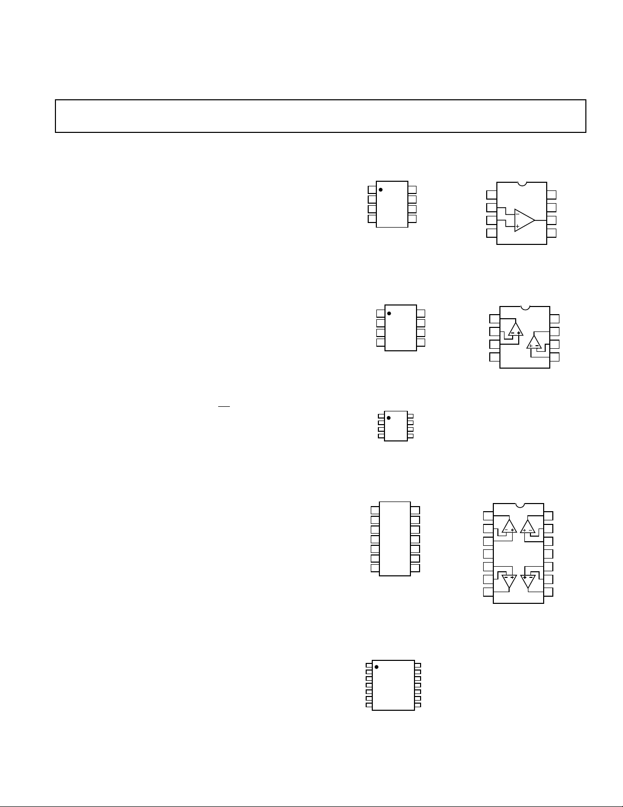
PIN CONFIGURATIONS
8-Lead Narrow-Body SO
8-Lead Narrow-Body SO
1
OUT A
2
–IN A
OP296
3
+IN A
4
V–
8-Lead TSSOP
14-Lead Narrow-Body SO
8
7
6
5
V+
OUT B
–IN B
+IN B
8-Lead Plastic DIP
1
NULL
–IN A
+IN A
V–
OP196
2
3
4
NC = NO CONNECT
8-Lead Plastic DIP
1
OUT A
–IN A
+IN A
V–
OP296
2
3
4
14-Lead Plastic DIP
8
7
6
5
8
7
6
5
NC
V+
OUT A
NULL
V+
OUT B
–IN B
+IN B
REV. B
Information furnished by Analog Devices is believed to be accurate and
reliable. However, no responsibility is assumed by Analog Devices for its
use, nor for any infringements of patents or other rights of third parties
which may result from its use. No license is granted by implication or
otherwise under any patent or patent rights of Analog Devices.
14-Lead TSSOP
(RU Suffix)
One Technology Way, P.O. Box 9106, Norwood, MA 02062-9106, U.S.A.
Tel: 781/329-4700 World Wide Web Site: http://www.analog.com
Fax: 781/326-8703 © Analog Devices, Inc., 1998
Page 2

OP196/OP296/OP496–SPECIFICATIONS
ELECTRICAL SPECIFICATIONS
(@ VS = +5.0 V, VCM = +2.5 V, TA = +258C unless otherwise noted)
Parameter Symbol Conditions Min Typ Max Units
INPUT CHARACTERISTICS
Offset Voltage V
OS
OP196G, OP296G, OP496G 35 300 µV
–40°C ≤ T
≤ +125°C 650 µV
A
OP296H, OP496H 800 µV
≤ +125°C 1.2 mV
A
±1.5 ±8nA
≤ +125°C ±20 nA
A
0 +5.0 V
Input Bias Current I
Input Offset Current I
Input Voltage Range V
B
OS
–40°C ≤ T
–40°C ≤ TA ≤ +125°C ±10 ±50 nA
–40°C ≤ T
CM
Common-Mode Rejection Ratio CMRR 0 V ≤ VCM ≤ 5.0 V,
≤ +125°C65 dB
A
≤ 4.7 V,
OUT
≤ +125°C 150 200 V/mV
A
Large Signal Voltage Gain A
Long-Term Offset Voltage V
VO
OS
–40°C ≤ T
RL = 100 kΩ,
0.30 V ≤ V
–40°C ≤ T
G Grade, Note 1 550 µV
H Grade, Note 1 1 mV
Offset Voltage Drift ∆V
/∆T G Grade, Note 2 1.5 µV/°C
OS
H Grade, Note 2 2 µV/°C
OUTPUT CHARACTERISTICS
Output Voltage Swing High V
Output Voltage Swing Low V
Output Current I
OH
OL
OUT
IL = –100 µA 4.85 4.92 V
= 1 mA 4.30 4.56 V
I
L
= 2 mA 4.1 V
I
L
IL = –1 mA 36 70 mV
= –1 mA 350 550 mV
I
L
= –2 mA 750 mV
I
L
±4mA
POWER SUPPLY
Power Supply Rejection Ratio PSRR ±2.5 V ≤ V
–40°C ≤ T
Supply Current per Amplifier I
SY
V
OUT
≤ ±6 V,
S
≤ +125°C85 dB
A
= 2.5 V, RL =
∞
60 µA
–40°C ≤ TA ≤ +125°C4580µA
DYNAMIC PERFORMANCE
Slew Rate SR R
= 100 kΩ 0.3 V/µs
L
Gain Bandwidth Product GBP 350 kHz
Phase Margin ø
m
47 Degrees
NOISE PERFORMANCE
Voltage Noise e
Voltage Noise Density e
Current Noise Density i
NOTES
1
Long-term offset voltage is guaranteed by a 1000 hour life test performed on three independent lots at +125°C, with an LTPD of 1.3.
2
Offset voltage drift is the average of the –40° C to +25°C delta and the +25° C to +125 ° C delta.
Specifications subject to change without notice.
p-p 0.1 Hz to 10 Hz 0.8 µV p-p
n
n
n
f = 1 kHz 26 nV/√Hz
f = 1 kHz 0.19 pA/√Hz
–2–
REV. B
Page 3

OP196/OP296/OP496
ELECTRICAL SPECIFICATIONS
(@ VS = +3.0 V, VCM = +1.5 V, TA = +258C unless otherwise noted)
Parameter Symbol Conditions Min Typ Max Units
INPUT CHARACTERISTICS
Offset Voltage V
OS
OP196G, OP296G, OP496G 35 300 µV
0°C ≤ T
≤ +125°C 650 µV
A
OP296H, OP496H 800 µV
≤ +125°C 1.2 mV
A
±10 ±50 nA
±1 ±8nA
0 +3.0 V
Input Bias Current I
Input Offset Current I
Input Voltage Range V
0°C ≤ T
B
OS
CM
Common-Mode Rejection Ratio CMRR 0 V ≤ VCM ≤ 3.0 V,
≤ +125°C60 dB
A
Large Signal Voltage Gain A
Long-Term Offset Voltage V
VO
OS
0°C ≤ T
RL = 100 kΩ 80 200 V/mV
G Grade, Note 1 550 µV
H Grade, Note 1 1 mV
Offset Voltage Drift ∆V
/∆T G Grade, Note 2 1.5 µV/°C
OS
H Grade, Note 2 2 µV/°C
OUTPUT CHARACTERISTICS
Output Voltage Swing High V
Output Voltage Swing Low V
OH
OL
IL = 100 µA 2.85 V
IL = –100 µA70mV
POWER SUPPLY
Supply Current per Amplifier I
SY
= 1.5 V, RL =
OUT
∞
40 60 µA
V
0°C ≤ TA ≤ +125°C80µA
DYNAMIC PERFORMANCE
Slew Rate SR R
= 100 kΩ 0.25 V/µs
L
Gain Bandwidth Product GBP 350 kHz
Phase Margin ø
m
45 Degrees
NOISE PERFORMANCE
Voltage Noise e
Voltage Noise Density e
Current Noise Density i
NOTES
1
Long-term offset voltage is guaranteed by a 1000 hour life test performed on three independent lots at +125°C, with an LTPD of 1.3.
2
Offset voltage drift is the average of the 0° C to +25°C delta and the +25°C to +125 ° C delta.
Specifications subject to change without notice.
p-p 0.1 Hz to 10 Hz 0.8 µV p-p
n
n
n
f = 1 kHz 26 nV/√Hz
f = 1 kHz 0.19 pA/√Hz
REV. B
–3–
Page 4

OP196/OP296/OP496
ELECTRICAL SPECIFICATIONS
(@ VS = +12.0 V, VCM = +6 V, TA = +258C unless otherwise noted)
Parameter Symbol Conditions Min Typ Max Units
INPUT CHARACTERISTICS
Offset Voltage V
OS
OP196G, OP296G, OP496G 35 300 µV
0°C ≤ T
≤ +125°C 650 µV
A
OP296H, OP496H 800 µV
≤ +125°C 1.2 mV
A
±1 ±8nA
≤ +125°C ±15 nA
A
0 +12 V
Input Bias Current I
Input Offset Current I
Input Voltage Range V
B
OS
0°C ≤ T
–40°C ≤ TA ≤ +125°C ±10 ±50 nA
–40°C ≤ T
CM
Common-Mode Rejection Ratio CMRR 0 V ≤ VCM ≤ +12 V,
≤ +125°C65 dB
A
Large Signal Voltage Gain A
Long-Term Offset Voltage V
VO
OS
–40°C ≤ T
RL = 100 kΩ 300 1000 V/mV
G Grade, Note 1 550 µV
H Grade, Note 1 1 mV
Offset Voltage Drift ∆V
/∆T G Grade, Note 2 1.5 µV/°C
OS
H Grade, Note 2 2 µV/°C
OUTPUT CHARACTERISTICS
Output Voltage Swing High V
Output Voltage Swing Low V
Output Current I
OH
OL
OUT
IL = 100 µA 11.85 V
= 1 mA 11.30 V
I
L
IL = –1 mA 70 mV
= –1 mA 550 mV
I
L
±4mA
POWER SUPPLY
Supply Current per Amplifier I
Supply Voltage Range V
SY
= 6 V, RL =
OUT
–40°C ≤ T
S
A
∞
60 µA
≤ +125°C80µA
+3 +12 V
V
DYNAMIC PERFORMANCE
Slew Rate SR R
= 100 kΩ 0.3 V/µs
L
Gain Bandwidth Product GBP 450 kHz
Phase Margin ø
m
50 Degrees
NOISE PERFORMANCE
Voltage Noise e
Voltage Noise Density e
Current Noise Density i
NOTES
1
Long-term offset voltage is guaranteed by a 1000 hour life test performed on three independent lots at +125°C, with an LTPD of 1.3.
2
Offset voltage drift is the average of the –40° C to +25°C delta and the +25° C to +125 ° C delta.
Specifications subject to change without notice.
p-p 0.1 Hz to 10 Hz 0.8 µV p-p
n
n
n
f = 1 kHz 26 nV/√Hz
f = 1 kHz 0.19 pA/√Hz
REV. B–4–
Page 5
OP196/OP296/OP496
WARNING!
ESD SENSITIVE DEVICE
ABSOLUTE MAXIMUM RATINGS
Supply Voltage . . . . . . . . . . . . . . . . . . . . . . . . . . . . . . . . .+15 V
Input Voltage
Differential Input Voltage
2
. . . . . . . . . . . . . . . . . . . . . . . . . . . . . . . . +15 V
2
. . . . . . . . . . . . . . . . . . . . . . .+15 V
1
Output Short Circuit Duration . . . . . . . . . . . . . . . . .Indefinite
Storage Temperature Range
P, S, RU Package . . . . . . . . . . . . . . . . . . . .–65°C to +150°C
Operating Temperature Range
OP196G, OP296G, OP496G, H . . . . . . . –40°C to +125°C
Junction Temperature Range
P, S, RU Package . . . . . . . . . . . . . . . . . . . –65°C to +150°C
Lead Temperature Range (Soldering, 60sec) . . . . . . . +300°C
Package Type u
3
JA
u
JC
Units
8-Lead Plastic DIP 103 43 °C/W
8-Lead SOIC 158 43 °C/W
8-Lead TSSOP 240 43 °C/W
14-Lead Plastic DIP 83 39 °C/W
14-Lead SOIC 120 36 °C/W
14-Lead TSSOP 180 35 °C/W
NOTES
1
Absolute maximum ratings apply to both DICE and packaged parts, unless
otherwise noted.
2
For supply voltages less than +15 V, the absolute maximum input voltage is
equal to the supply voltage.
3
θJA is specified for the worst case conditions, i.e., θJA is specified for device in
socket for P-DIP package; θJA is specified for device soldered in circuit board
for SOIC and TSSOP packages.
ORDERING GUIDE
Temperature Package Package
Model Range Description Option
OP196GP –40°C to +125°C 8-Lead Plastic DIP N-8
OP196GS –40°C to +125°C 8-Lead SOIC SO-8
OP296GP –40°C to +125°C 8-Lead Plastic DIP N-8
OP296GS –40°C to +125°C 8-Lead SOIC SO-8
OP296HRU –40°C to +125°C 8-Lead TSSOP RU-8
OP496GP –40°C to +125°C 14-Lead Plastic DIP N-14
OP496GS –40°C to +125°C 14-Lead SOIC SO-14
OP496HRU –40°C to +125°C 14-Lead TSSOP RU-14
CAUTION
ESD (electrostatic discharge) sensitive device. Electrostatic charges as high as 4000 V readily
accumulate on the human body and test equipment and can discharge without detection.
Although the OP196/OP296/OP496 feature proprietary ESD protection circuitry, permanent
damage may occur on devices subjected to high energy electrostatic discharges. Therefore, prope r
ESD precautions are recommended to avoid performance degradation or loss of functionalit y .
REV. B –5–
Page 6

OP196/OP296/OP496–Typical Performance Characteristics
TEMPERATURE – 8C
INPUT OFFSET VOLTAGE – mV
600
400
–400
–75 150–50 –25 0 25 50 75 100 125
200
0
–200
13V VS 112V
V
CM
=
V
S
2
250
VS = 13V
T
200
150
100
QUANTITY – Amplifiers
50
0
–250 250–200
–150 –100 –50 0 50 100 150 200
INPUT OFFSET VOLTAGE – mV
= 1258C
A
COUNT = 400
Figure 1. Input Offset Voltage Distribution
250
VS = 15V
T
200
150
100
QUANTITY – Amplifiers
50
= 1258C
A
COUNT = 400
25
20
15
10
QUANTITY – Amplifiers
5
0
–4.0 1.0–3.5
–3.0 –2.5 –2.0 –1.5 –1.0 –0.5 0 0.5
INPUT OFFSET DRIFT, TCVOS – mV/8C
VS = 15V
V
= 12.5V
CM
= –408C TO 11258C
T
A
Figure 4. Input Offset Voltage Distribution (TCVOS)
25
20
15
10
QUANTITY – Amplifiers
5
VS = 112V
= 16V
V
CM
= –408C TO 11258C
T
A
0
–250 250–200
–150 –100 –50 0 50 100 150 200
INPUT OFFSET VOLTAGE – mV
Figure 2. Input Offset Voltage Distribution
250
VS = 112V
T
200
150
100
QUANTITY – Amplifiers
50
0
–250 250–200
–150 –100 –50 0 50 100 150 200
INPUT OFFSET VOLTAGE – mV
= 1258C
A
COUNT = 400
Figure 3. Input Offset Voltage Distribution
0
–4.0 1.0–3.5
–3.0 –2.5 –2.0 –1.5 –1.0 –0.5 0 0.5
INPUT OFFSET DRIFT, TCVOS – mV/8C
1.5
Figure 5. Input Offset Voltage Distribution (TCVOS)
Figure 6. Input Offset Voltage vs. Temperature
–6–
REV. B
Page 7

25
LOAD CURRENT – mA
1000
100
1
0.001 100.01
OUTPUT VOLTAGE – mV
0.1 1
10
SOURCE
SINK
VS = 61.5V
LOAD CURRENT – mA
1000
100
1
0.001 100.01
OUTPUT VOLTAGE – mV
0.1 1
10
SOURCE
SINK
VS = 62.5V
LOAD CURRENT – mA
1000
100
1
0.001 100.01
OUTPUT VOLTAGE – mV
0.1 1
10
SOURCE
SINK
VS = 66V
VS = 15V
V
= 12.5V
20
15
10
5
INPUT BAIS CURRENT – nA
0
–75 150–50 –25 0 25 50 75 100 125
TEMPERATURE – 8C
CM
Figure 7. Input Bias Current vs. Temperature
16
12
OP196/OP296/OP496
Figure 10. Output Voltage to Supply Rail vs. Load Current
8
INPUT BIAS CURRENT – nA
4
2123
SUPPLY VOLTAGE – Volts
5
14
Figure 8. Input Bias Current vs. Supply Voltage
40
30
20
10
0
–10
–20
INPUT BIAS CURRENT – nA
–30
–40
–2.5 2.5–2.0
–1.5 –1.0 –0.5 0 0.5 1.0 1.5 2.0
COMMON-MODE VOLTAGE – Volts
VS = 62.5V
= 1258C
T
A
Figure 9. Input Bias Current vs. Common-Mode Voltage
Figure 11. Output Voltage to Supply Rail vs. Load Current
Figure 12. Output Voltage to Supply Rail vs. Load Current
REV. B –7–
Page 8

FREQUENCY – Hz
90
80
–10
10 1M100
OPEN-LOOP GAIN – dB
1k 10k 100k
70
60
50
40
30
20
10
0
225
PHASE SHIFT – 8C
0
45
90
135
180
VS = 62.5V
T
A
= –408C
GAIN
PHASE
FREQUENCY – Hz
90
80
–10
10 1M100
OPEN-LOOP GAIN – dB
1k 10k 100k
70
60
50
40
30
20
10
0
225
PHASE SHIFT – 8C
0
45
90
135
180
VS = 62.5V
T
A
= 11258C
PHASE
GAIN
TEMPERATURE – 8C
950
800
200
–75 150–50
OPEN-LOOP GAIN – V/mV
–25 0 25 50 75 100 125
650
500
350
VS = 15V
0.3V
< V
O
< 4.7V
R
L
= 100kV
OP196/OP296/OP496–Typical Performance Characteristics
4.95
4.70
4.45
4.2
–75 150–50
VS = 15V
–25 0 25 50 75 100 125
OUTPUT VOLTAGE – Volts
3.85
OH
V
3.7
IL = 100mA
IL = 1mA
IL = 2mA
TEMPERATURE – 8C
Figure 13. Output Voltage Swing vs. Temperature
0.80
0.60
IL = –1mA
0.50
VS = 15V
Figure 16. Open-Loop Gain and Phase vs. Frequency
(No Load)
OUTPUT VOLTAGE – Volts
OL
V
Figure 14. Output Voltage Swing vs. Temperature
Figure 15. Open-Loop Gain and Phase vs. Frequency
(No Load)
0.30
0.10
–75 150–50
90
80
70
60
50
40
30
20
OPEN-LOOP GAIN – dB
10
0
–10
10 1M100
–25 0 25 50 75 100 125
IL = –100mA
TEMPERATURE – 8C
GAIN
PHASE
1k 10k 100k
FREQUENCY – Hz
VS = 62.5V
T
= 1258C
A
0
45
90
135
180
225
Figure 17. Open-Loop Gain and Phase vs. Frequency
(No Load)
PHASE SHIFT – 8C
Figure 18. Open-Loop Gain vs. Temperature
REV. B–8–
Page 9

600
FREQUENCY – Hz
CMRR – dB
140
–40
100 10M1k 10k 100k 1M
120
100
80
60
40
20
0
–20
VS = 62.5V
T
A
= 1258C
ALL CHANNELS
160
PSRR – dB
FREQUENCY – Hz
160
140
–40
10 10M100 1k 10k 1M100k
120
100
80
60
40
20
0
–20
VS = 15V
T
A
= 1258C
+PSRR
–PSRR
OP196/OP296/OP496
500
400
300
200
OPEN-LOOP GAIN – V/mV
100
0
150 1100 50 10 2
LOAD – kV
VS = 15V
TA = 1258C
Figure 19. Open Loop Gain vs. Resistive Load
70
60
50
40
30
20
10
0
CLOSED-LOOP GAIN – dB
–10
–20
–30
10 1M100
1k 10k 100k
FREQUENCY – Hz
VS = 62.5V
R
= 10kV
L
T
= 1258C
A
Figure 20. Closed-Loop Gain vs. Frequency
Figure 22. CMRR vs. Frequency
Figure 23. PSRR vs. Frequency
1000
900
800
700
600
500
400
300
OUTPUT IMPEDANCE – V
200
100
REV. B –9–
Figure 21. Output Impedance vs. Frequency
VS = 62.5V
T
= 1258C
A
0
100 1M1k
ACL = 10
10k 100k
FREQUENCY – Hz
ACL = 1
6
VS = 62.5V
= 15V p-p
V
100k
IN
A
V
R
L
= 11
= 100kV
5
4
3
2
1
MAXIMUM OUTPUT SWING – Volts
0
1k 1M10k
FREQUENCY – Hz
Figure 24. Maximum Output Swing vs. Frequency
Page 10

FREQUENCY – Hz
0.6
0.5
0
11k10
CURRENT NOISE DENSITY – pA/ Hz
100
0.4
0.3
0.2
0.1
VS = 62.5V
T
A
= 1258C
V
CM
= 0V
SETTLING TIME – ms
10
–10
0305
INPUT STEP – Volts
10 15 20 25
8
2
–4
–6
–8
6
4
0
–2
1OUTPUT SWING
– OUTPUT SWING
VS = 66V
TA = 1258C
TO 0.1%
10
0%
100
90
1s
2mV
VS = 62.5V
A
V
= 10k
e
n
= 0.8mV p-p
OP196/OP296/OP496–Typical Performance Characteristics
90
80
70
60
50
/AMPLIFIER – mA
SY
I
40
30
VS = 13V
VS = 112V
VS = 15V
20
–75 150–50
–40 –25 0 25 50 85 75 100 125
TEMPERATURE – 8C
Figure 25. Supply Current/Amplifier vs. Temperature
55
TA = 1258C
50
45
/AMPLIFIER – mA
40
SY
I
35
1133
5791112
SUPPLY VOLTAGE – Volts
Figure 26. Supply Current/Amplifier vs. Supply Voltage
80
70
60
VS = 62.5V
= 1258C
T
A
= 0V
V
CM
Figure 28. Input Bias Current Noise Density vs. Frequency
Figure 29. Settling Time to 0.1% vs. Step Size
50
40
30
20
10
VOLTAGE NOISE DENSITY – nV/ Hz
0
11k10 100
Figure 27. Voltage Noise Density vs. Frequency
FREQUENCY – Hz
–10–
Figure 30. 0.1 Hz to 10 Hz Noise
REV. B
Page 11

1x
1x
2x
2x
Q8
Q7
Q6
Q5
R4A
R4B
I2
1x1x
Q4
Q3
2x2x
Q2
Q1
R3A
R3B
Q9
I3
Q13
Q11
D3
Q12
QC1
Q10
QC2
Q15
CC1
Q14
R2
R1
I1 R6
CF1
D4
Q17
D5
Q18
R5
R7
QL1
Q16
CF2
D6
Q19
2x 1x
I4
CC2
D7
1*
5*
Q20
1.5x1xD10
R9
D8
Q21
R8
D9
Q22
Q23
I5
OUT
+IN
–IN
V
EE
V
CC
*OP196 ONLY
100mV
10
0%
100
90
1V
VS = 62.5V
RL = 10kV
10ms
OP196/OP296/OP496
100
90
VS = 2.5V
20mV
AV = 1
RL = 10kV
CL = 100pF
TA = 1258C
2ms
10
0%
0V
Figure 31. Small Signal Transient Response
100
100mV
90
VS = 62.5V
= 1
A
20mV
V
R
L
C
L
T
A
= 100kV
= 100pF
= 1258C
2ms
10
0%
0V
Figure 32. Small Signal Transient Response
CH A: 40.0mV FS 5.00mV/DIV
MKR: 36.8mV/ Hz
Figure 33. Large Signal Transient Response
VS = 62.5V
= 100kV
100
90
10
0%
1V
R
L
10ms
Figure 34. Large Signal Transient Response
0Hz
MKR: 1.00Hz BW: 145mHz
10Hz
Figure 35. 1/f Noise Corner, VS = ±5 V, AV = 1,000
REV. B –11–
Figure 36. Simplified Schematic
Page 12

OP196/OP296/OP496
10
0%
100
90
VS = 5V
A
V
= 1
5V
1ms
5V
0
0
V
IN
V
OUT
VOLTAGE – 5V/DIV
TIME – 1ns/DIV
6
7
2
3
V–
V+
OP196
100kV
4
1
5
OP296
C
F
V
IN
R
G
R
F
R
X
C
L
V
OUT
RX = WHERE RO = OPEN-LOOP OUTPUT RESISTANCE
R
O RG
R
F
C
F
=
I
+ ( ) ( )
CL R
O
I
|
A
CL
|
R
F
+
R
G
R
F
APPLICATIONS INFORMATION
Functional Description
The OP196 family of operational amplifiers is comprised of singlesupply, micropower, rail-to-rail input and output amplifiers. Input
offset voltage (V
) is only 300 µV maximum, while the output
OS
will deliver ±5 mA to a load. Supply current is only 50 µA, while
bandwidth is over 450 kHz and slew rate is 0.3 V/µs. Figure 36
is a simplified schematic of the OP196—it displays the novel
circuit design techniques used to achieve this performance.
Input Overvoltage Protection
The OPx96 family of op amps uses a composite PNP/NPN
input stage. Transistor Q1 in Figure 36 has a collector-base
voltage of 0 V if +IN = V
. If +IN then exceeds VEE, the junc-
EE
tion will be forward biased and large diode currents will flow,
which may damage the device. The same situation applies to
+IN on the base of transistor Q5 being driven above V
. There-
CC
fore, the inverting and noninverting inputs must not be driven
above or below either supply rail unless the input current is
limited.
Figure 37 shows the input characteristics for the OPx96 family.
This photograph was generated with the power supply pins
connected to ground and a curve tracer’s collector output drive
connected to the input. As shown in the figure, when the input
voltage exceeds either supply by more than 0.6 V, internal pn-
junctions energize and permit current flow from the inputs to
the supplies. If the current is not limited, the amplifier may be
damaged. To prevent damage, the input current should be
limited to no more than 5 mA.
input current must be limited if the inputs are driven beyond the
supply rails. In the circuit of Figure 38, the source amplitude is
±15 V, while the supply voltage is only ±5 V. In this case, a
2 kΩ source resistor limits the input current to 5 mA.
Figure 38. Output Voltage Phase Reversal Behavior
Input Offset Voltage Nulling
The OP196 provides two offset adjust terminals that can be
used to null the amplifier’s internal V
. In general, operational
OS
amplifier terminals should never be used to adjust system offset
voltages. A 100 kΩ potentiometer, connected as shown in Figure 39, is recommended to null the OP196’s offset voltage.
Offset nulling does not adversely affect TCV
performance,
OS
providing that the trimming potentiometer temperature coefficient does not exceed ±100 ppm/°C.
8
6
100
90
4
2
0
–2
10
–4
INPUT CURRENT – mA
0%
–6
–8
–1.5 –1 –0.5 0 0.5 1 1.5
INPUT VOLTAGE – Volts
Figure 37. Input Overvoltage I-V Characteristics of the
OPx96 Family
Output Phase Reversal
Some other operational amplifiers designed for single-supply
operation exhibit an output voltage phase reversal when their
inputs are driven beyond their useful common-mode range.
Typically for single-supply bipolar op amps, the negative supply
determines the lower limit of their common-mode range. With
these common-mode limited devices, external clamping diodes
are required to prevent input signal excursions from exceeding
the device’s negative supply rail (i.e., GND) and triggering
output phase reversal.
The OPx96 family of op amps is free from output phase reversal
effects due to its novel input structure. Figure 38 illustrates the
performance of the OPx96 op amps when the input is driven
beyond the supply rails. As previously mentioned, amplifier
Figure 39. Offset Nulling Circuit
Driving Capacitive Loads
OP196 family amplifiers are unconditionally stable with capacitive loads less than 170 pF. When driving large capacitive loads
in unity-gain configurations, an in-the-loop compensation
technique is recommended, as illustrated in Figure 40.
Figure 40. In-the-Loop Compensation Technique for
Driving Capacitive Loads
REV. B–12–
Page 13

OP196/OP296/OP496
59kV
1/2
OP296/
OP496
100kV
100kV
FREQ OUT
f
OSC
= < 200Hz @ V+ = +5V
1
RC
C
V+
R
2
3
4
8
1
A Micropower False-Ground Generator
Some single supply circuits work best when inputs are biased
above ground, typically at 1/2 of the supply voltage. In these
cases, a false-ground can be created by using a voltage divider
buffered by an amplifier. One such circuit is shown in Figure 41.
This circuit will generate a false-ground reference at 1/2 of the
supply voltage, while drawing only about 55 µA from a 5 V
supply. The circuit includes compensation to allow for a 1 µF
bypass capacitor at the false-ground output. The benefit of a
large capacitor is that not only does the false-ground present a
very low dc resistance to the load, but its ac impedance is low
as well.
+5V OR +12V
10kV
2
OP196
3
7
4
0.022mF
6
100V
+2.5V OR +6V
1mF
240kV
240kV
1mF
Figure 41. A Micropower False-Ground Generator
Single-Supply Half-Wave and Full-Wave Rectifiers
An OP296, configured as a voltage follower operating from a
single supply, can be used as a simple half-wave rectifier in low
frequency (<400 Hz) applications. A full-wave rectifier can be
configured with a pair of OP296s as illustrated in Figure 42.
same potential. The result is that both terminals of R1 are at the
same potential and no current flows in R1. Since there is no
current flow in R1, the same condition must exist in R2; thus,
the output of the circuit tracks the input signal. When the input
signal is below 0 V, the output voltage of A1 is forced to 0 V.
This condition now forces A2 to operate as an inverting voltage
follower because the noninverting terminal of A2 is also at 0 V.
The output voltage of V
A is then a full-wave rectified
OUT
version of the input signal. A resistor in series with A1’s
noninverting input protects the ESD diodes when the input
signal goes below ground.
Square Wave Oscillator
The oscillator circuit in Figure 43 demonstrates how a rail-torail output swing can reduce the effects of power supply variations on the oscillator’s frequency. This feature is especially
valuable in battery powered applications, where voltage regulation may not be available. The output frequency remains stable
as the supply voltage changes because the RC charging current,
which is derived from the rail-to-rail output, is proportional to
the supply voltage. Since the Schmitt trigger threshold level is
also proportional to supply voltage, the frequency remains relatively independent of supply voltage. For a supply voltage
change from 9 V to 5 V, the output frequency only changes
about 4 Hz. The slew rate of the amplifier limits the oscillation
frequency to a maximum of about 200 Hz at a supply voltage
of +5 V.
+2Vp-p
<500Hz
(HALF-WAVE
(FULL-WAVE
2kV
INPUT
V
OUT
OUTPUT)
V
OUT
OUTPUT)
R1
100kV
+5V
8
3
1
A1
4
2
1/2
OP296
500mV1V
100
90
B
10
A
0%
500mV
6
5
R2
100kV
A2
7
1/2
OP296
f = 500Hz
500µs
A
V
OUT
FULL-WAVE
RECTIFIED
OUTPUT
V
B
OUT
HALF-WAVE
RECTIFIED
OUTPUT
Figure 42. Single-Supply Half-Wave and Full-Wave
Rectifiers Using an OP296
The circuit works as follows: When the input signal is above
0 V, the output of amplifier A1 follows the input signal. Since
the noninverting input of amplifier A2 is connected to A1’s
output, op amp loop control forces A2’s inverting input to the
Figure 43. Square Wave Oscillator Has Stable Frequency
Regardless of Supply Voltage Changes
A 3 V Low Dropout, Linear Voltage Regulator
Figure 44 shows a simple +3 V voltage regulator design. The
regulator can deliver 50 mA load current while allowing a 0.2 V
dropout voltage. The OP296’s rail-to-rail output swing easily
drives the MJE350 pass transistor without requiring special
drive circuitry. With no load, its output can swing to less than
the pass transistor’s base-emitter voltage, turning the device
nearly off. At full load, and at low emitter-collector voltages, the
transistor beta tends to decrease. The additional base current is
easily handled by the OP296 output.
The AD589 provides a 1.235 V reference voltage for the regulator. The OP296, operating with a noninverting gain of 2.43,
drives the base of the MJE350 to produce an output voltage of
3.0 V. Since the MJE350 operates in an inverting (commonemitter) mode, the output feedback is applied to the OP296’s
noninverting input.
REV. B –13–
Page 14

OP196/OP296/OP496
8
1
234
1/2
OP296
+5V
+5V
S
G
D
M1
3N163
MONITOR
OUTPUT
R2
2.49kV
R1
100V
R
SENSE
0.1V
I
L
+5V
< 50mA
I
V
5V TO 3.2V
MJE 350
IN
8
3
1/2
1
OP296
2
4
1000pF
43kV
1.235V
AD589
44.2kV
1%
30.9kV
1%
L
V
O
100mF
Figure 44. 3 V Low Dropout Voltage Regulator
Figure 45 shows the regulator’s recovery characteristics when its
output underwent a 20 mA to 50 mA step current change.
STEP
CURRENT
CONTROL
WAVEFORM
50mA
30mA
OUTPUT
2V
100
90
10
0%
10mV
50µs
Figure 45. Output Step Load Current Recovery
Buffering a DAC Output
Multichannel TrimDACs® such as the AD8801/AD8803, are
widely used for digital nulling and similar applications. These
DACs have rail-to-rail output swings, with a nominal output
resistance of 5 kΩ. If a lower output impedance is required, an
OP296 amplifier can be added. Two examples are shown in
Figure 45. One amplifier of an OP296 is used as a simple buffer
to reduce the output resistance of DAC A. The OP296 provides
rail-to-rail output drive while operating down to a 3 V supply
and requiring only 50 µA of supply current.
The next two DACs, B and C, sum their outputs into the other
OP296 amplifier. In this circuit DAC C provides the coarse
output voltage setting and DAC B is used for fine adjustment.
The insertion of R1 in series with DAC B attenuates its contribution to the voltage sum node at the DAC C output.
A High-Side Current Monitor
In the design of power supply control circuits, a great deal of
design effort is focused on ensuring a pass transistor’s long-term
reliability over a wide range of load current conditions. As a
result, monitoring and limiting device power dissipation is of
prime importance in these designs. The circuit illustrated in
Figure 47 is an example of a +5 V, single-supply high-side current monitor that can be incorporated into the design of a voltage regulator with fold-back current limiting or a high current
power supply with crowbar protection. This design uses an
OP296’s rail-to-rail input voltage range to sense the voltage
drop across a 0.1 Ω current shunt. A p-channel MOSFET is
used as the feedback element in the circuit to convert the op
amp’s differential input voltage into a current. This current is
then applied to R2 to generate a voltage that is a linear representation of the load current. The transfer equation for the current
monitor is given by:
Monitor Output = R2 ×
R
SENSE
R1
× I
L
For the element values shown, the Monitor Output’s transfer
characteristic is 2.5 V/A.
+5V
V
V
DD
REFH
V
H
V
L
V
H
V
L
V
H
V
L
AD8801/
AD8803
V
GND
REFL
DIGITAL INTERFACING
OMITTED FOR CLARITY
TrimDAC is a registered trademark of Analog Devices Inc.
Figure 46. Buffering a TrimDAC Output
R1
100kV
OP296
SIMPLE BUFFER
0V TO +5V
+4.983V
+1.1mV
SUMMER CIRCUIT
WITH FINE TRIM
ADJUSTMENT
Figure 47. A High-Side Load Current Monitor
A Single-Supply RTD Amplifier
The circuit in Figure 48 uses three op amps on the OP496 to
produce a bridge driver for an RTD amplifier while operating
from a single +5 V supply. The circuit takes advantage of the
OP496’s wide output swing to generate a bridge excitation
voltage of 3.9 V. An AD589 provides a 1.235 V reference for
the bridge current. Op amp A1 drives the bridge to maintain
1.235 V across the parallel combination of the 6.19 kΩ and
2.55 MΩ resistors, which generates a 200 µA current source.
This current divides evenly and flows through both halves of
the bridge. Thus, 100 µA flows through the RTD to generate
an output voltage which is proportional to its resistance. For
improved accuracy, a 3-wire RTD is recommended to balance
the line resistance in both 100 Ω legs of the bridge.
REV. B–14–
Page 15

OP196/OP296/OP496
100V
2.55MV
6.17kV
AD589
26.7kV
RTD
200V
10-TURNS
26.7kV
37.4kV
+5V
100V
1/4
OP496
A1
A2
100kV
NOTE:
ALL RESISTORS 1% OR BETTER
1/4
OP496
392V
20kV
GAIN = 259
392V
+5V
A3
100kV
0.1mF
1/4
OP496
V
OUT
Figure 48. A Single Supply RTD Amplifier
* OP496 SPICE Macro-model REV. B, 5/95
* ARG / ADSC
*
* Copyright 1995 by Analog Devices
*
* Refer to “README.DOC” file for License Statement.
* Use of this model indicates your acceptance of the
* terms and provisions in the License Statement.
*
* Node assignments
* Noninverting input
* Inverting input
* Positive supply
* Negative supply
* Output
*
*
.SUBCKT OP496 1 2 99 50 49
*
* INPUT STAGE
*
IREF 21 50 1U
QB1 21 21 99 99 QP 1
QB2 22 21 99 99 QP 1
QB34 219999QP1.5
QB4 22 22 50 50 QN 2
QB5 11 22 50 50 QN 3
Q154750QN2
Q264850QN2
Q344750QN1
Q444850QN1
Q5501799QP2
Q6503899QP2
EOS 3 2 POLY(1) (17,98) 35U 1
Q7991950QN2
Q8993 1050QN2
Q9 12 11 9 99 QP 2
Q10 13 11 10 99 QP 2
Q11 11 11 9 99 QP 1
Q12 11 11 10 99 QP 1
R1 99 5 50K
R2 99 6 50K
R3 12 50 50K
R4 13 50 50K
IOS 1 2 0.75N
C10 5 6 3.183P
C11 12 13 3.183P
Amplifiers A2 and A3 are configured in a two op amp instrumentation amplifier configuration. For ease of measurement,
the IA resistors are chosen to produce a gain of 259, so that
each 1°C increase in temperature results in a 10 mV increase in
the output voltage. To reduce measurement noise, the bandwidth of the amplifier is limited. A 0.1 µF capacitor, connected
in parallel with the 100 kΩ resistor on amplifier A3, creates a pole
at 16 Hz.
CIN 1 2 1P
*
* GAIN STAGE
*
EREF 98 0 POLY(2) (99,0) (50,0) 0 0.5 0.5
G1 98 15 POLY(2) (6,5) (13,12) 0 10U10U
R10 15 98 251.641MEG
CC 15 49 8P
D1 15 99 DX
D2 50 15 DX
*
* COMMON MODE STAGE
*
ECM 16 98 POLY(2) (1,98) (2,98) 0 0.5 0.5
R11 16 17 1MEG
R12 17 98 10
*
* OUTPUT STAGE
*
ISY 99 50 20U
EIN 35 50 POLY(1) (15,98) 1.42735 1
Q24 37 35 36 50 QN 1
QD4 37 37 38 99 QP 1
Q27 40 37 38 99 QP 1
R5 36 39 150K
R6 99 38 45K
Q26 39 42 50 50 QN 3
QD5 40 40 39 50 QN 1
Q28 41 40 44 50 QN 1
QL1 37 41 99 99 QP 1
R7 99 41 10.7K
I4 99 43 2U
QD7 42 42 50 50 QN 2
QD6 43 43 42 50 QN 2
Q29 47 43 44 50 QN 1
Q30 44 45 50 50 QN 1.5
QD10 45 46 50 50 QN 1
R9 45 46 175
Q31 46 47 48 99 QP 1
QD8 47 47 48 99 QP 1
QD9 48 48 51 99 QP 5
R8 99 51 2.9K
I5 99 46 1U
Q32 49 48 99 99 QP 10
Q33 49 44 50 50 QN 4
.MODEL DX D()
.MODEL QN NPN(BF=120VAF=100)
.MODEL QP PNP(BF=80 VAF=60)
.ENDS
REV. B –15–
Page 16

OP196/OP296/OP496
14
17
8
0.795 (20.19)
0.725 (18.42)
0.280 (7.11)
0.240 (6.10)
PIN 1
SEATING
PLANE
0.022 (0.558)
0.014 (0.356)
0.060 (1.52)
0.015 (0.38)
0.210 (5.33)
MAX
0.130
(3.30)
MIN
0.070 (1.77)
0.045 (1.15)
0.100
(2.54)
BSC
0.160 (4.06)
0.115 (2.93)
0.325 (8.25)
0.300 (7.62)
0.015 (0.381)
0.008 (0.204)
0.195 (4.95)
0.115 (2.93)
14 8
71
0.3444 (8.75)
0.3367 (8.55)
0.2440 (6.20)
0.2284 (5.80)
0.1574 (4.00)
0.1497 (3.80)
PIN 1
SEATING
PLANE
0.0098 (0.25)
0.0040 (0.10)
0.0192 (0.49)
0.0138 (0.35)
0.0688 (1.75)
0.0532 (1.35)
0.0500
(1.27)
BSC
0.0099 (0.25)
0.0075 (0.19)
0.0500 (1.27)
0.0160 (0.41)
8°
0°
0.0196 (0.50)
0.0099 (0.25)
x 45°
14 8
7
1
0.201 (5.10)
0.193 (4.90)
0.256 (6.50)
0.246 (6.25)
0.177 (4.50)
0.169 (4.30)
PIN 1
SEATING
PLANE
0.006 (0.15)
0.002 (0.05)
0.0118 (0.30)
0.0075 (0.19)
0.0256
(0.65)
BSC
0.0433
(1.10)
MAX
0.0079 (0.20)
0.0035 (0.090)
0.028 (0.70)
0.020 (0.50)
8°
0°
OUTLINE DIMENSIONS
Dimensions shown in inches and (mm).
0.210 (5.33)
MAX
0.160 (4.06)
0.115 (2.93)
0.022 (0.558)
0.014 (0.356)
0.1574 (4.00)
0.1497 (3.80)
0.0098 (0.25)
0.0040 (0.10)
8-Lead Plastic DIP
(N-8)
0.430 (10.92)
0.348 (8.84)
8
5
0.280 (7.11)
BSC
0.240 (6.10)
0.060 (1.52)
0.015 (0.38)
0.070 (1.77)
0.045 (1.15)
0.130
(3.30)
MIN
SEATING
PLANE
14
PIN 1
0.100
(2.54)
8-Lead Narrow Body SOIC
(SO-8)
0.1968 (5.00)
0.1890 (4.80)
8
5
0.2440 (6.20)
41
0.2284 (5.80)
PIN 1
0.0688 (1.75)
0.0532 (1.35)
0.325 (8.25)
0.300 (7.62)
0.015 (0.381)
0.008 (0.204)
0.0196 (0.50)
0.0099 (0.25)
14-Lead Plastic DIP
(N-14)
C2051b–0–2/98
0.195 (4.95)
0.115 (2.93)
14-Lead Narrow-Body SOIC
(SO-14)
x 45°
PLANE
0.177 (4.50)
PIN 1
SEATING
PLANE
0.0500
(1.27)
BSC
0.122 (3.10)
0.114 (2.90)
8
0.169 (4.30)
1
0.0256 (0.65)
0.0118 (0.30)
0.0075 (0.19)
SEATING
0.006 (0.15)
0.002 (0.05)
0.0192 (0.49)
0.0138 (0.35)
8-Lead TSSOP
(RU-8)
5
0.256 (6.50)
4
BSC
0.0433
(1.10)
MAX
0.0098 (0.25)
0.0075 (0.19)
0.246 (6.25)
0.0079 (0.20)
0.0035 (0.090)
8°
0°
0.028 (0.70)
8°
0°
0.020 (0.50)
0.0500 (1.27)
0.0160 (0.41)
14-Lead TSSOP
(RU-14)
PRINTED IN U.S.A.
REV. B–16–
 Loading...