

Page 1
Dual/Quad Rail-to-Rail
a
FEATURES
Rail-to-Rail Output Swing
Single-Supply Operation: +3 V to +36 V
Low Offset Voltage: 300 mV
Gain Bandwidth Product: 75 kHz
High Open-Loop Gain: 1000 V/mV
Unity-Gain Stable
Low Supply Current/Per Amplifier: 150 mA max
APPLICATIONS
Battery Operated Instrumentation
Servo Amplifiers
Actuator Drives
Sensor Conditioners
Power Supply Control
GENERAL DESCRIPTION
Rail-to-rail output swing combined with dc accuracy are the key
features of the OP495 quad and OP295 dual CBCMOS operational amplifiers. By using a bipolar front end, lower noise and
higher accuracy than that of CMOS designs has been achieved.
Both input and output ranges include the negative supply, providing the user “zero-in/zero-out” capability. For users of 3.3
volt systems such as lithium batteries, the OP295/OP495 is
specified for three volt operation.
Maximum offset voltage is specified at 300 µV for +5 volt opera-
tion, and the open-loop gain is a minimum of 1000 V/mV. This
yields performance that can be used to implement high accuracy
systems, even in single supply designs.
The ability to swing rail-to-rail and supply +15 mA to the load
makes the OP295/OP495 an ideal driver for power transistors
and “H” bridges. This allows designs to achieve higher efficiencies and to transfer more power to the load than previously possible without the use of discrete components. For applications
Operational Amplifiers
OP295/OP495
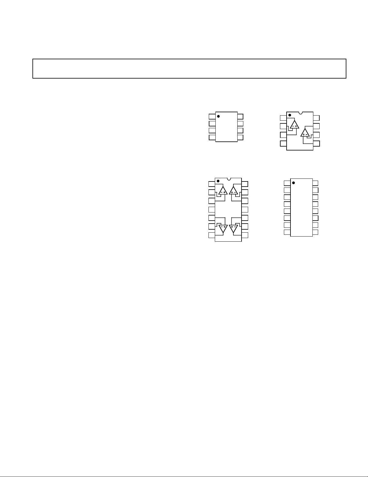
PIN CONNECTIONS
8-Lead Narrow-Body SO 8-Lead Epoxy DIP
(S Suffix) (P Suffix)
OP495
8
V+
7
OUT B
–IN B
6
+IN B
OUT D
14
–IN D
13
+IN D
12
11
V–
10
+IN C
9
–IN C
OUT C
8
OUT A
–IN A
+IN A
V–
OUT A
–IN A
+IN A
V+
+IN B
–IN B
OUT B
NC
1
2
3
4
OP295
1
2
3
413
OP495
5
6
7
89
NC = NO CONNECT
8
V+
OUT B
7
6
–IN B
+IN B
5
OUT D
16
–IN D
15
14
+IN D
V–
12
+IN C
11
–IN C
10
OUT C
NC
OUT A
1
2
–IN A
+IN A
OP295
3
45
V–
14-Lead Epoxy DIP 16-Lead SO (300 Mil)
(P Suffix) (S Suffix)
OUT A
1
2
–IN A
+IN A
3
4
V+
5
+IN B
6
–IN B
OUT B
7
that require driving inductive loads, such as transformers, increases in efficiency are also possible. Stability while driving
capacitive loads is another benefit of this design over CMOS
rail-to-rail amplifiers. This is useful for driving coax cable or
large FET transistors. The OP295/OP495 is stable with loads in
excess of 300 pF.
The OP295 and OP495 are specified over the extended industrial (–40°C to +125°C) temperature range. OP295s are available in 8-pin plastic and ceramic DIP plus SO-8 surface mount
packages. OP495s are available in 14-pin plastic and SO-16
surface mount packages. Contact your local sales office for
MIL-STD-883 data sheet.
REV. B
Information furnished by Analog Devices is believed to be accurate and
reliable. However, no responsibility is assumed by Analog Devices for its
use, nor for any infringements of patents or other rights of third parties
which may result from its use. No license is granted by implication or
otherwise under any patent or patent rights of Analog Devices.
© Analog Devices, Inc., 1995
One Technology Way, P.O. Box 9106, Norwood. MA 02062-9106, U.S.A.
Tel: 617/329-4700 Fax: 617/326-8703
Page 2

OP295/OP495–SPECIFICA TIONS
ELECTRICAL CHARACTERISTICS
Parameter Symbol Conditions Min Typ Max Units
INPUT CHARACTERISTICS
Offset Voltage V
Input Bias Current I
Input Offset Current I
Input Voltage Range V
Common-Mode Rejection Ratio CMRR 0 V ≤ VCM ≤ 4.0 V, –40°C ≤ TA ≤ +125°C 90 110 dB
Large Signal Voltage Gain A
Offset Voltage Drift ∆VOS/∆T 15 µV/°C
OUTPUT CHARACTERISTICS
Output Voltage Swing High V
Output Voltage Swing Low V
Output Current I
POWER SUPPLY
Power Supply Rejection Ratio PSRR ±1.5 V ≤ VS ≤ ±15 V 90 110 dB
Supply Current Per Amplifier I
DYNAMIC PERFORMANCE
Skew Rate SR RL = 10 kΩ 0.03 V/µs
Gain Bandwidth Product GBP 75 kHz
Phase Margin θ
NOISE PERFORMANCE
Voltage Noise en
Voltage Noise Density e
Current Noise Density i
Specifications subject to change without notice.
OS
B
OS
CM
VO
OH
OL
OUT
SY
O
p-p
n
n
(@ VS = +5.0 V, VCM = +2.5 V, TA = +258C unless otherwise noted)
–40°C ≤ TA ≤ +125°C 800 µV
–40°C ≤ TA ≤ +125°C30nA
–40°C ≤ TA ≤ +125°C ±5nA
0 +4.0 V
RL = 10 kΩ, 0.005 ≤ V
RL = 10 kΩ, –40°C ≤ TA ≤ +125°C 500 V/mV
≤ 4.0 V 1000 10,000 V/mV
OUT
RL = 100 kΩ to GND 4.98 5.0 V
RL = 10 kΩ to GND 4.90 4.94 V
I
= 1 mA, –40°C ≤ TA ≤ +125°C 4.7 V
OUT
RL = 100 kΩ to GND 0.7 2 mV
RL = 10 kΩ to GND 0.7 2 mV
I
= 1 mA, –40°C ≤ TA ≤ +125°C90mV
OUT
± 11 ± 18 mA
±1.5 V ≤ VS ≤ ±15 V,
–40°C ≤ TA ≤ +125°C85dB
V
= 2.5 V, RL = ∞, –40°C ≤ TA ≤ +125°C 150 µA
OUT
0.1 Hz to 10 Hz 1.5 µV p-p
f = 1 kHz 51 nV/√Hz
f = 1 kHz <0.1 pA/√Hz
30 300 µV
820 nA
±1 ±3nA
86 Degrees
ELECTRICAL CHARACTERISTICS
(@ VS = +3.0 V, VCM = +1.5 V, TA = +258C unless otherwise noted)
Parameter Symbol Conditions Min Typ Max Units
INPUT CHARACTERISTICS
Offset Voltage V
Input Bias Current I
Input Offset Current I
Input Voltage Range V
Common-Mode Rejection Ratio CMRR 0 V ≤ VCM ≤ 2.0 V, –40°C ≤ TA ≤ +125°C 90 110 dB
Large Voltage Gain A
Offset Voltage Drift ∆VOS/∆T 1 µV/°C
OS
B
OS
CM
VO
RL = 10 kΩ 750 V/mV
0 +2.0 V
30 500 µV
820 nA
±1 ±3nA
OUTPUT CHARACTERISTICS
Output Voltage Swing High V
Output Voltage Swing Low V
OH
OL
RL = 10 kΩ to GND 2.9 V
RL = 10 kΩ to GND 0.7 2 mV
POWER SUPPLY
Power Supply Rejection Ratio PSRR ±1.5 V ≤ VS ≤ ±15 V 90 110 dB
±1.5 V ≤ VS ≤ ±15 V,
–40°C ≤ TA ≤ +125°C85dB
Supply Current Per Amplifier I
SY
V
= 1.5 V, RL = ∞, –40°C ≤ TA ≤ +125°C 150 µA
OUT
DYNAMIC PERFORMANCE
Slew Rate SR RL = 10 kΩ 0.03 V/µs
Gain Bandwidth Product GBP 75 kHz
Phase Margin θ
O
85 Degrees
NOISE PERFORMANCE
Voltage Noise en
Voltage Noise Density e
Current Noise Density i
Specifications subject to change without notice.
p-p
n
n
0.1 Hz to 10 Hz 1.6 µV p-p
f = 1 kHz 53 nV/√Hz
f = 1 kHz <0.1 pA/√Hz
–2–
REV. B
Page 3

OP295/OP495
ELECTRICAL CHARACTERISTICS
Parameter Symbol Conditions Min Typ Max Units
INPUT CHARACTERISTICS
Offset Voltage V
Input Bias Current I
Input Offset Current I
Input Voltage Range V
Common-Mode Rejection Ratio CMRR –15.0 V ≤ VCM ≤ +13.5 V, –40°C ≤ TA ≤ +125°C 90 110 dB
Large Signal Voltage Gain A
Offset Voltage Drift ∆VOS/∆T 1 µV/°C
OUTPUT CHARACTERISTICS
Output Voltage Swing High V
Output Voltage Swing Low V
Output Current I
POWER SUPPLY
Power Supply Rejection Ratio PSRR VS = ±1.5 V to ±15 V 90 110 dB
Supply Current I
Supply Voltage Range V
DYNAMIC PERFORMANCE
Slew Rate SR RL = 10 kΩ 0.03 V/µs
Gain Bandwidth Product GBP 85 kHz
Phase Margin θ
NOISE PERFORMANCE
Voltage Noise e
Voltage Noise Density e
Current Noise Density i
Specifications subject to change without notice.
OS
B
OS
CM
VO
OH
OL
OUT
SY
S
O
n p-p
n
n
(@ VS = ±15.0 V, TA = +258C unless otherwise noted)
–40°C ≤ TA ≤ +125°C 800 µV
VCM = 0 V 7 20 nA
VCM = 0 V, –40°C ≤ TA ≤ +125°C30nA
VCM = 0 V ±1 ±3nA
V
= 0 V, –40°C ≤ TA ≤ +125°C ±5nA
CM
RL = 10 kΩ 1000 4000 V/mV
RL = 100 kΩ to GND 14.95 V
RL = 10 kΩ to GND 14.80 V
RL = 100 kΩ to GND –14.95 V
RL = 10 kΩ to GND –14.85 V
VS = ±1.5 V to ±15 V, –40°C ≤ TA ≤ +125°C85 dB
VO = 0 V, RL = ∞, VS = ±18 V,
–40°C ≤ TA ≤ +125°C 175 µA
0.1 Hz to 10 Hz 1.25 µV p-p
f =1 kHz 45 nV/√Hz
f = 1 kHz <0.1 pA/√Hz
–15 +13.5 V
± 15 ±25 mA
+3 (±1.5) +36 (±18) V
30 300 µV
83 Degrees
W AFER TEST LIMITS
(@ VS = +5.0 V, VCM = 2.5 V, TA = +258C unless otherwise noted)
Parameter Symbol Conditions Limit Units
Offset Voltage Vos 300 µV max
Input Bias Current I
Input Offset Current I
Input Voltage Range
1
Common-Mode Rejection Ratio CMRR 0 V ≤ V
Power Supply Rejection Ratio PSRR ±1.5 V ≤ V
Large Signal Voltage Gain A
Output Voltage Swing High V
Supply Current Per Amplifier I
NOTES
Electrical tests and wafer probe to the limits shown. Due to variations in assembly methods and normal yield loss, yield after packaging is not guaranteed for standard
product dice. Consult factory to negotiate specifications based on dice lot qualifications through sample lot assembly and testing.
1
Guaranteed by CMRR test.
B
OS
V
SY
CM
VO
OH
RL = 10 kΩ 1000 V/mV min
RL = 10 kΩ 4.9 V min
V
OUT
≤ 4 V 90 dB min
CM
≤ ±15 V 90 µV/V
S
= 2.5 V, RL = ∞ 150 µA max
20 nA max
±2 nA max
0 to +4 V min
ORDERING GUIDE
Temperature Package Package
Model Range Description Option
OP295GP –40°C to +125°C 8-Pin Plastic DIP N-8
OP295GS –40°C to +125°C 8-Pin SOIC SO-8
OP295GBC +25°C DICE
Model Range Description Option
OP495GP –40°C to +125°C 14-Pin Plastic DIP N-14
OP495GS –40°C to +125°C 16-Pin SOL R-16
OP495GBC +25°C DICE
Temperature Package Package
REV. B
–3–
Page 4
OP295/OP495
15.2
–15.2
100
–14.6
–15.0
–25
–14.8
–50
14.2
–14.4
14.4
14.6
14.8
15.0
7550250
TEMPERATURE – °C
– OUTPUT SWING – Volts
+ OUTPUT SWING – Volts
VS = ±15V
RL = 100k
RL = 2k
RL = 2k
RL = 100k
RL = 10k
RL = 10k
ABSOLUTE MAXIMUM RATINGS
Supply Voltage . . . . . . . . . . . . . . . . . . . . . . . . . . . . . . . . .±18 V
Input Voltage
Differential Input Voltage
2
. . . . . . . . . . . . . . . . . . . . . . . . . . . . . . . . .±18 V
2
. . . . . . . . . . . . . . . . . . . . . . . +36 V
1
Output Short-Circuit Duration . . . . . . . . . . . . . . . . . Indefinite
Storage Temperature Range
P, S Package . . . . . . . . . . . . . . . . . . . . . . . .–65°C to +150°C
Operating Temperature Range
OP295G, OP495G . . . . . . . . . . . . . . . . . . .–40°C to +125°C
Junction Temperature Range
P, S Package . . . . . . . . . . . . . . . . . . . . . . . .–65°C to +150°C
Lead Temperature Range (Soldering, 60 Sec) . . . . . . . +300°C
Package Type u
3
JA
u
JC
Unit
8-Pin Plastic DIP (P) 103 43 °C/W
8-Pin SOIC (S) 158 43 °C/W
14-Pin Plastic DIP (P) 83 39 °C/W
16-Pin SO (S) 98 30 °C/W
NOTES
1
Absolute maximum ratings apply to both DICE and packaged parts, unless
otherwise noted.
2
For supply voltages less than ±18 V, the absolute maximum input voltage is equal
to the supply voltage.
3
θJA is specified for the worst case conditions, i.e., θJA is specified for device in socket
for cerdip, P-DIP, and LCC packages; θJA is specified for device soldered in circuit
board for SOIC package.
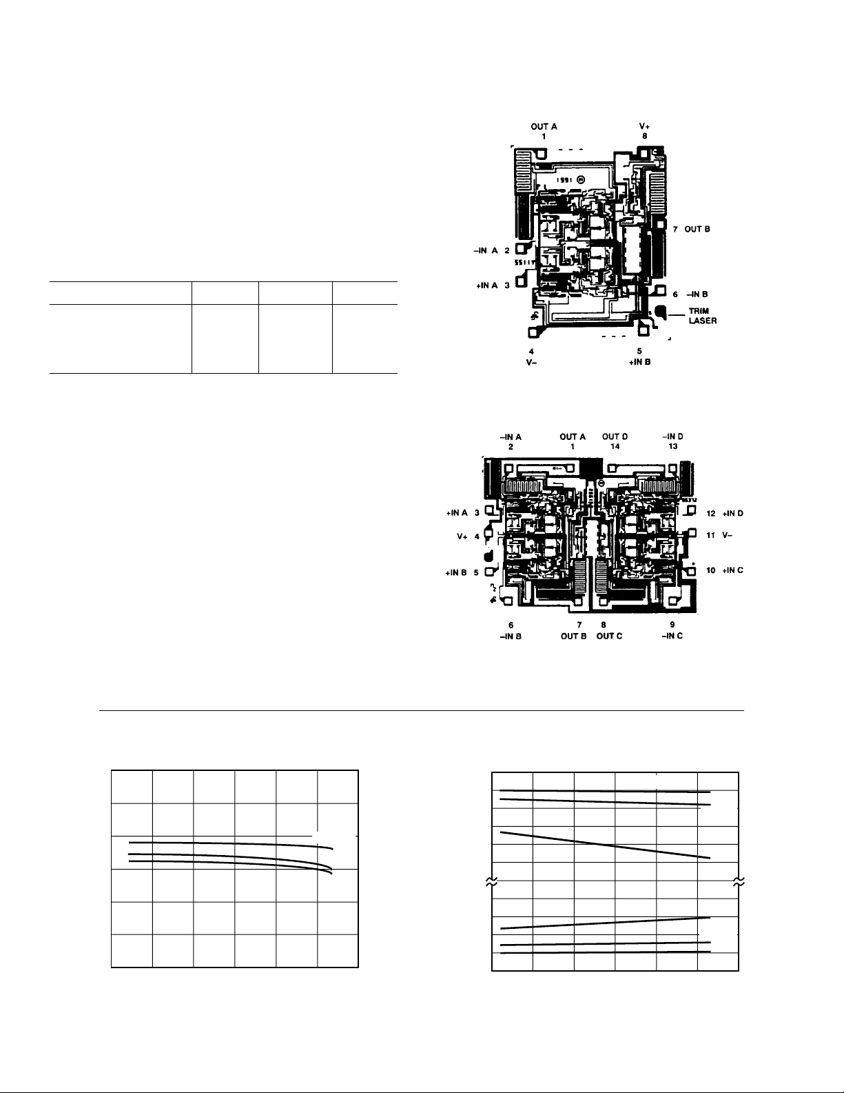
DICE CHARACTERISTICS
OP295 Die Size 0.066 × 0.080 inch, 5,280 sq. mils.
Substrate (Die Backside) Is Connected to V+.
Transistor Count, 74.
Typical Characteristics
140
120
100
80
60
40
SUPPLY CURRENT PER AMPLIFIER – µA
20
–50
–25
Supply Current Per Amplifier vs. Temperature Output Voltage Swing vs. Temperature
TEMPERATURE – °C
VS = +36V
VS = +5V
VS = +3V
7550250
100
–4–
OP495 Die Size 0.113 × 0.083 inch, 9,380 sq. mils.
Substrate (Die Backside) Is Connected to V+.
Transistor Count, 196.
REV. B
Page 5
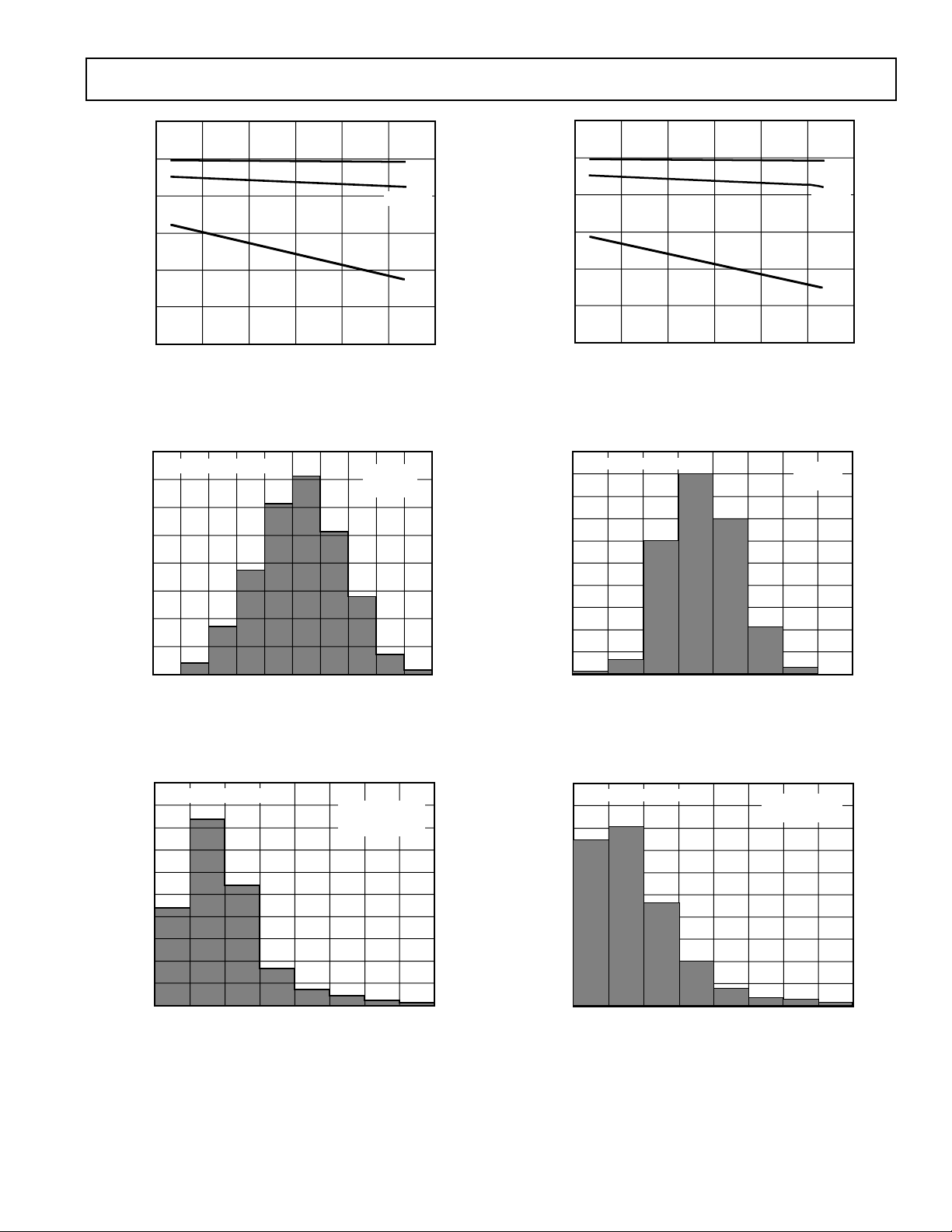
Typical Characteristics–OP295/OP495
500
0
3.2
150
50
0.4
100
0
300
200
250
350
400
450
2.82.42.01.61.20.8
TC – VOS – µV/°C
UNITS
VS = +5V
–40° ≤ TA ≤ +85°C
BASED ON 1200 OP AMPS
3.10
3.00
2.90
2.80
2.70
OUTPUT VOLTAGE SWING – Volts
2.60
2.50
–50
–25
TEMPERATURE – °C
Output Voltage Swing vs. Temperature
200
BASED ON 600 OP AMPS
175
150
125
100
UNITS
75
50
25
0
–200–250
INPUT OFFSET VOLTAGE – µV
RL = 100k
RL = 10k
7550250
VS = +5V
= +25°C
T
A
VS = +3V
RL = 2k
200150100500–50–100–150
250
100
5.10
5.00
4.90
4.80
4.70
OUTPUT VOLTAGE SWING – Volts
4.60
4.50
–50
–25
TEMPERATURE – °C
Output Voltage Swing vs. Temperature
500
BASED ON 1200 OP AMPS
450
400
350
300
250
UNITS
200
150
100
50
0
–50
–100
INPUT OFFSET VOLTAGE – µV
VS = +5V
RL = 100k
RL = 10k
RL = 2k
7550250
VS = +5V
= +25°C
T
A
250200150100500
100
300
REV. B
OP295 Input Offset (VOS) Distribution
250
BASED ON 600 OP AMPS
225
200
175
150
125
UNITS
100
75
50
25
0
0
0.4
– VOS – µV/°C
T
C
OP295 TC–VOS Distribution
VS = +5V
–40° ≤ T
≤ +85°C
A
OP495 Input Offset (VOS) Distribution
3.2
2.82.42.01.61.20.8
OP495 TC–VOS Distribution
–5–
Page 6
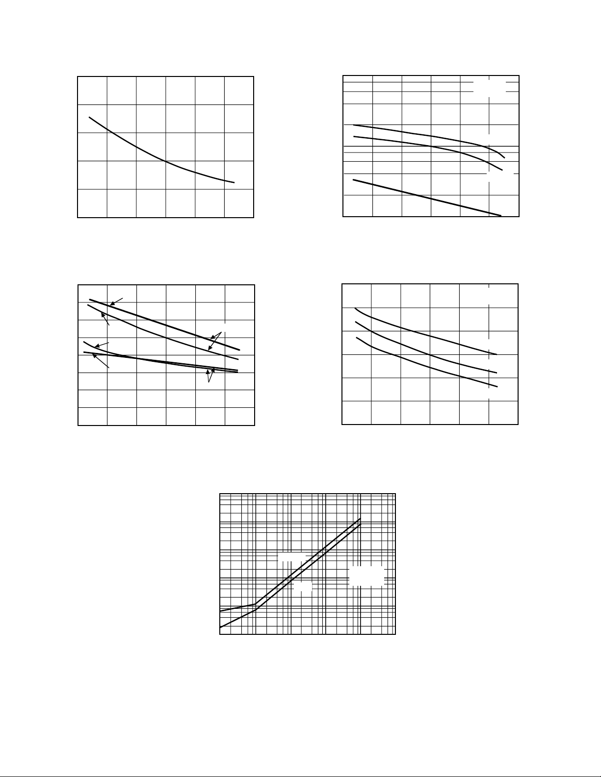
OP295/OP495–Typical Characteristics
20
16
12
8
INPUT BIAS CURRENT – nA
4
0
–50
–25
TEMPERATURE – °C
Input Bias Current vs. Temperature
40
35
30
25
20
15
OUTPUT CURRENT – mA
10
5
SOURCE
SINK
SOURCE
SINK
VS = ±15V
VS = +5V
VS = +5V
7550250
100
100
10
OPEN-LOOP GAIN – V/µV
1
–50 25
–25
TEMPERATURE – °C
Open-Loop Gain vs. Temperature
12
10
8
6
4
OPEN-LOOP GAIN – V/µV
2
50
VS = ±15V
VO = ±10V
RL = 100k
RL = 10k
RL = 2k
75
VS = +5V
VO = +4V
RL = 100k
RL = 10k
RL = 2k
1000
0
–25–50
TEMPERATURE – °C
Output Current vs. Temperature
0
100
7550250
–50
–25
Open-Loop Gain vs. Temperature
1V
100mV
10mV
OUTPUT VOLTAGE ∆ TO RAIL
1mV
100µV
1µA10µA 10mA1mA100µA
SOURCE
SINK
LOAD CURRENT
VS = +5V
= +25°C
T
A
Output Voltage to Supply Rail vs. Load Current
TEMPERATURE – °C
100
7550250
REV. B–6–
Page 7
OP295/OP495
MAT- 03
5
6
3
2
1
7
R3
R4
Q1
Q2
R1
R6
10Ω
V
OUT
LED
1
8
4
3
2
R5
10kΩ
C2
10µF
R7
510Ω
C1
1500pF
R8
100Ω
R2
27kΩ
V
IN
0.1µF
10µF
Q2
2N3906
OP295/
OP495
APPLICATIONS
Rail-to-Rail Applications Information
The OP295/OP495 has a wide common-mode input range extending from ground to within about 800 mV of the positive
supply. There is a tendency to use the OP295/OP495 in buffer
applications where the input voltage could exceed the commonmode input range. This may initially appear to work because of
the high input range and rail-to-rail output range. But above the
common-mode input range the amplifier is, of course, highly
nonlinear. For this reason it is always required that there be
some minimal amount of gain when rail-to-rail output swing is
desired. Based on the input common-mode range this gain
should be at least 1.2.
Low Drop-Out Reference
The OP295/OP495 can be used to gain up a 2.5 V or other low
voltage reference to 4.5 volts for use with high resolution A/D
converters that operate from +5 volt only supplies. The circuit
in Figure 1 will supply up to 10 mA. Its no-load drop-out voltage is only 20 mV. This circuit will supply over 3.5 mA with a
+5 volt supply.
16k
+5V
2
REF43
4
6
20k
1/2
OP295/
OP495
0.001µF
+5V
10Ω
1 TO 10µF
V
= 4.5V
OUT
Figure 1. 4.5 Volt, Low Drop-Out Reference
Low Noise, Single Supply Preamplifier
Most single supply op amps are designed to draw low supply
current, at the expense of having higher voltage noise. This
tradeoff may be necessary because the system must be powered
by a battery. However, this condition is worsened because all
circuit resistances tend to be higher; as a result, in addition to
the op amp’s voltage noise, Johnson noise (resistor thermal
noise) is also a significant contributor to the total noise of the
system.
The choice of monolithic op amps that combine the characteristics of low noise and single supply operation is rather limited.
Most single supply op amps have noise on the order of 30 nV/√
to 60 nV/√
5 nV/√
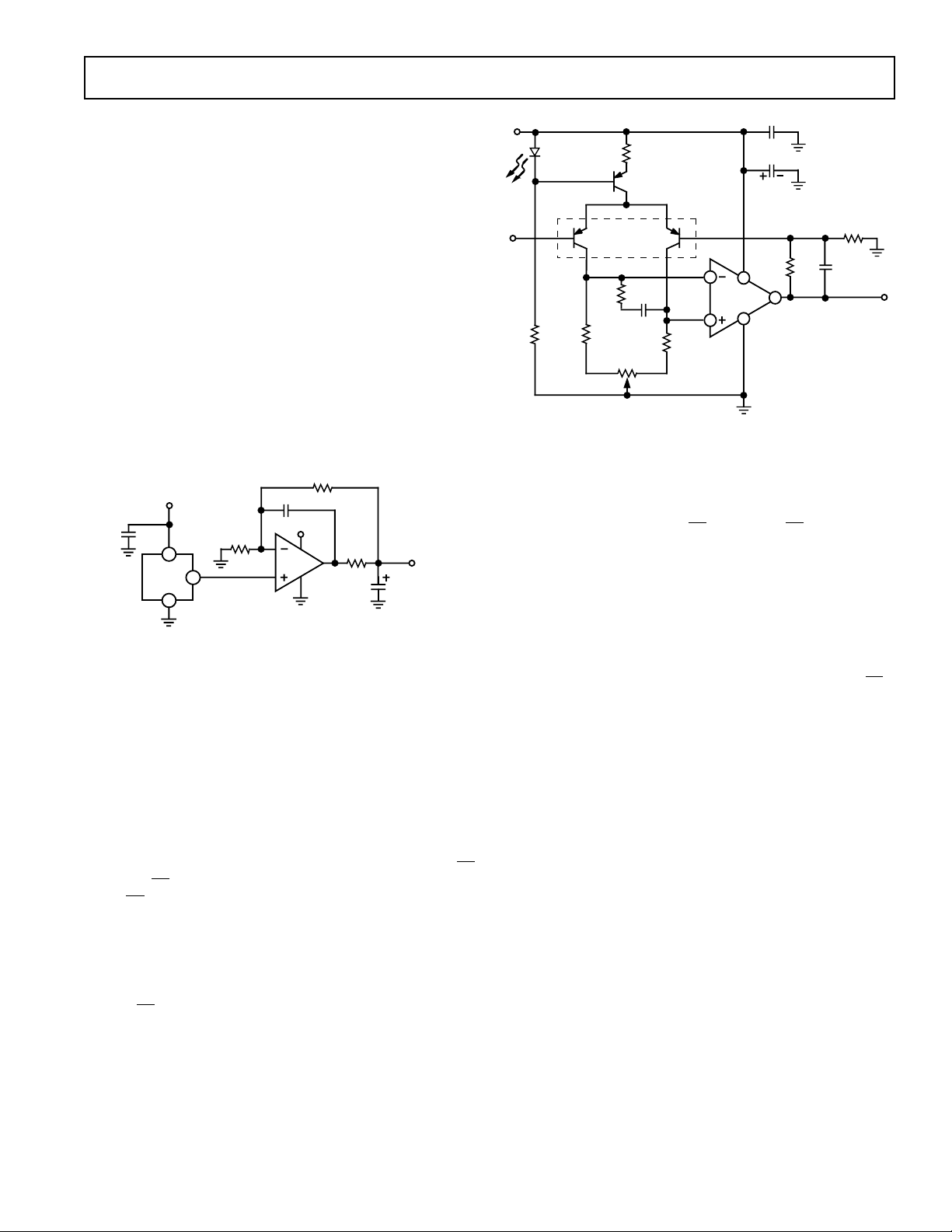
In order to achieve both low noise and low supply voltage operation, discrete designs may provide the best solution. The circuit
on Figure 2 uses the OP295/OP495 rail-to-rail amplifier and a
matched PNP transistor pair—the MAT03—to achieve zero-in/
zero-out single supply operation with an input voltage noise of
3.1 nV/√
this circuit ideal for maximizing dynamic range when amplifying
low level signals in single supply applications. The OP295/OP495
provides rail-to-rail output swings, allowing this circuit to operate with 0 to 5 volt outputs. Only half of the OP295/OP495 is
used, leaving the other uncommitted op amp for use elsewhere.
Hz and single supply amplifiers with noise below
Hz do not exist.
Hz at 100 Hz. R5 and R6 set the gain of 1000, making
Hz
Figure 2. Low Noise Single Supply Preamplifier
The input noise is controlled by the MAT03 transistor pair and
the collector current level. Increasing the collector current reduces the voltage noise. This particular circuit was tested with
1.85 mA and 0.5 mA of current. Under these two cases, the input voltage noise was 3.1 nV/√
Hz and 10 nV/√Hz, respectively.
The high collector currents do lead to a tradeoff in supply current, bias current, and current noise. All of these parameters will
increase with increasing collector current. For example, typically
the MAT03 has an h
= 165. This leads to bias currents of
FE
11 µA and 3 µA, respectively. Based on the high bias currents,
this circuit is best suited for applications with low source impedance such as magnetic pickups or low impedance strain gages.
Furthermore, a high source impedance will degrade the noise
performance. For example, a 1 kΩ resistor generates 4 nV/√
Hz
of broadband noise, which is already greater than the noise of
the preamp.
The collector current is set by R1 in combination with the LED
and Q2. The LED is a 1.6 V “Zener” that has a temperature coefficient close to that of Q2’s base-emitter junction, which provides a constant 1.0 V drop across R1. With R1 equal to 270 Ω,
the tail current is 3.7 mA and the collector current is half that,
or 1.85 mA. The value of R1 can be altered to adjust the collector current. Whenever R1 is changed, R3 and R4 should also be
adjusted. To maintain a common-mode input range that includes ground, the collectors of the Q1 and Q2 should not go
above 0.5 V—otherwise they could saturate. Thus, R3 and R4
have to be small enough to prevent this condition. Their values
and the overall performance for two different values of R1 are
summarized in Table I. Lastly, the potentiometer, R8, is needed
to adjust the offset voltage to null it to zero. Similar performance can be obtained using an OP90 as the output amplifier
with a savings of about 185 µA of supply current. However, the
output swing will not include the positive rail, and the bandwidth will reduce to approximately 250 Hz.
REV. B
–7–
Page 8
OP295/OP495
V+
V
IN
V
REF
1
R1
100k
R2
20k
R3
20k
R4
100k
V
O
VIN + V
REF
VO = 5 +
200k
R
G
(
)
R
G
3
2
8
7
4
5
6
1/2
OP295/
OP495
1/2
OP295/
OP495
Table I. Single Supply Low Noise Preamp Performance
IC = 1.85 mA IC = 0.5 mA
R1 270 Ω 1.0 kΩ
R3, R4 200 Ω 910 Ω
e
@ 100 Hz 3.15 nV/√Hz 8.6 nV/√Hz
n
e
@ 10 Hz 4.2 nV/√Hz 10.2 nV/√Hz
n
I
SY
I
B
4.0 mA 1.3 mA
11 µA3 µA
Bandwidth 1 kHz 1 kHz
Closed-Loop Gain 1000 1000
Driving Heavy Loads
The OP295/OP495 is well suited to drive loads by using a
power transistor, Darlington or FET to increase the current to
the load. The ability to swing to either rail can assure that the
device is turned on hard. This results in more power to the load
and an increase in efficiency over using standard op amps with
their limited output swing. Driving power FETs is also possible
with the OP295/OP495 because of its ability to drive capacitive
loads of several hundred picofarads without oscillating.
Without the addition of external transistors the OP295/OP495
can drive loads in excess of ± 15 mA with ±15 or +30 volt
supplies. This drive capability is somewhat decreased at lower
supply voltages. At ±5 volt supplies the drive current is ±11 mA.
Driving motors or actuators in two directions in a single supply
application is often accomplished using an “H” bridge. The
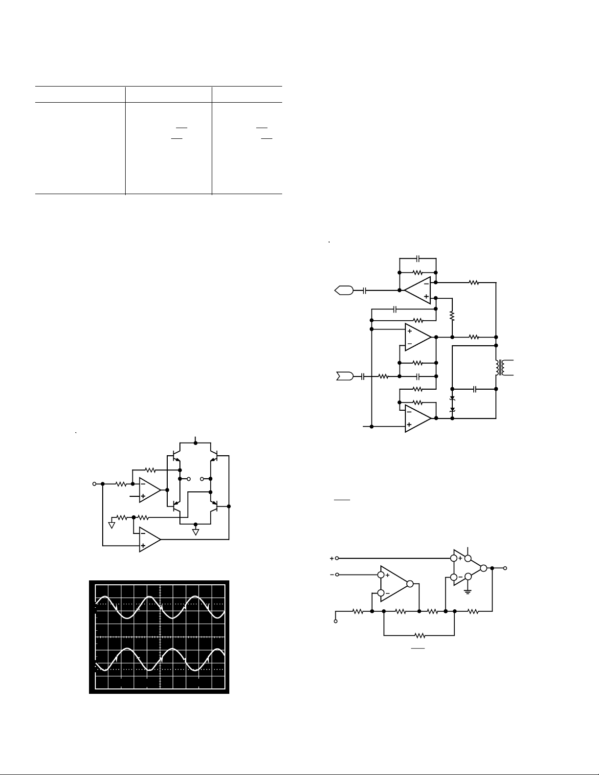
principle is demonstrated in Figure 3a. From a single +5 volt
supply this driver is capable of driving loads from 0.8 V to 4.2 V
in both directions. Figure 3b shows the voltages at the inverting
and noninverting outputs of the driver. There is a small crossover
glitch that is frequency dependent and would not cause problems
+5V
2N2222 2N2222
0 ≤ V
≤ 2.5V
IN
5k
1.67V
10k
10k
10k
2N2907
OUTPUTS
2N2907
unless this was a low distortion application such as audio. If this
is used to drive inductive loads, be sure to add diode clamps to
protect the bridge from inductive kickback.
Direct Access Arrangement
OP295/OP495 can be used in a single supply Direct Access Arrangement (DAA) as is shown an in Figure 4. This figure shows
a portion of a typical DM capable of operating from a single
+5 volt supply and it may also work on +3 volt supplies with
minor modifications. Amplifiers A2 and A3 are configured so
that the transmit signal TXA is inverted by A2 and is not inverted by A3. This arrangement drives the transformer differentially so that the drive to the transformer is effectively doubled
over a single amplifier arrangement. This application takes advantage of the OP295/OP495’s ability to drive capacitive loads,
and to save power in single supply applications.
390pF
37.4kΩ
RXA
TXA
2.5V REF
0.1µF
0.1µF
0.0047µF
OP295/
OP495
OP295/
OP495
A1
3.3kΩ
A2
22.1kΩ
750pF20kΩ
20kΩ
20kΩ
A3
OP295/
OP495
20kΩ
20kΩ
475Ω
0.033µF
1:1
Figure 4. Direct Access Arrangement
A Single Supply Instrumentation Amplifier
The OP295/OP495 can be configured as a single supply instrumentation amplifier as in Figure 5. For our example, V
equal to
put common-mode voltage range includes ground and the out-
V+
and VO is measured with respect to V
2
REF
. The in-
REF
is set
put swings to both rails.
Figure 3a. “H” Bridge
100
90
10
0%
2V
Figure 3b. “H” Bridge Outputs
2V 1ms
Figure 5. Single Supply Instrumentation Amplifier
Resistor RG sets the gain of the instrumentation amplifier. Minimum gain is 6 (with no R
). All resistors should be matched in
G
absolute value as well as temperature coefficient to maximize
–8–
REV. B
Page 9
OP295/OP495
+5V
R2
41.2k
R3
5kΩ
R4
100kΩ
V
DD R
FB
V
REF
SRICLKGND
I
OUT
DAC8043
3
4
7
65
1
2
8
+5V
DIGITAL
CONTROL
+5V
AD589
R1
17.8kΩ
+1.23V
LD
VO = (4.096V)
D
4096
TOTAL POWER DISSIPATION = 1.6mW
8
1
4
2
3
OP295/
OP495
8
1
2
3
220pF
220Ω
REF02
GND
62
4
100Ω
2N1711
100k
1%
HP
5082-2800
100Ω
1%
V
IN
0 + 3V
100kΩ
10-TURN
1.21M
1%
NULL ADJ
SPAN ADJ
182k
1%
10kΩ
10-TURN
5V
+12V
TO
+36V
R
L
100Ω
4–20mA
4
1/2
OP295/
OP495
common-mode rejection performance and minimize drift. This
instrumentation amplifier can operate from a supply voltage as
low as 3 volts.
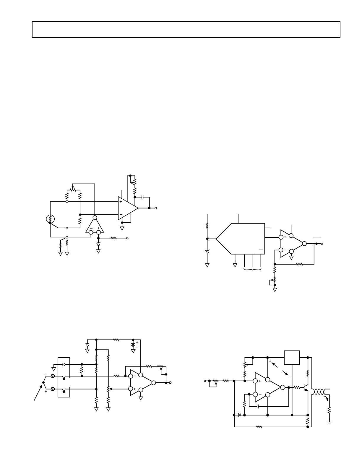
A Single Supply RTD Thermometer Amplifier
This RTD amplifier takes advantage of the rail-to-rail swing of
the OP295/OP495 to achieve a high bridge voltage in spite of a
low 5 V supply. The OP295/OP495 amplifier servos a constant
200 µA current to the bridge. The return current drops across
the parallel resistors 6.19 kΩ and the 2.55 MΩ, developing a
voltage that is servoed to 1.235 V, which is established by the
AD589 bandgap reference. The 3-wire RTD provides an equal
line resistance drop in both 100 Ω legs of the bridge, thus improving the accuracy.
The AMP04 amplifies the differential bridge signal and converts
it to a single-ended output. The gain is set by the series resistance of the 332 Ω resistor plus the 50 Ω potentiometer. The
gain scales the output to produce a 4.5 V full scale. The
0.22 µF capacitor to the output provides a 7 Hz low-pass filter
to keep noise at a minimum.
ZERO ADJ
10-TURNS
26.7k
100Ω
RTD
2.55M
1%
0.5%
200Ω
100Ω
0.5%
6.19k
1%
26.7k
0.5%
AD589
1
2 3
1/2
OP295/
OP495
1.235
37.4k
+5V
7
3
2
1
AMP04
4
5
+5V
8
50Ω
332Ω
0.22µF
6
V
4.5V = 450°C
0V = 0°C
O
To calibrate, immerse the thermocouple measuring junction in a
0°C ice bath, adjust the 500 Ω Zero Adjust pot to zero volts out.
Then immerse the thermocouple in a 250°C temperature bath
or oven and adjust the Scale Adjust pot for an output voltage of
2.50 V, which is equivalent to 250°C. Within this temperature
range, the K-type thermocouple is quite accurate and produces
a fairly linear transfer characteristic. Accuracy of ±3°C is achievable without linearization.
Even if the battery voltage is allowed to decay to as low as 7 volts,
the rail-to-rail swing allows temperature measurements to
700°C. However, linearization may be necessary for temperatures above 250°C where the thermocouple becomes rather
nonlinear. The circuit draws just under 500 µA supply current
from a 9 V battery.
A 5 V Only, 12-Bit DAC That Swings 0 V to 4.095 V
Figure 8 shows a complete voltage output DAC with wide output voltage swing operating off a single +5 V supply. The serial
input 12-bit D/A converter is configured as a voltage output
device with the 1.235 V reference feeding the current output pin
(I
) of the DAC. The V
OUT
which is normally the input now
REF
becomes the output.
The output voltage from the DAC is the binary weighted volt-
age of the reference, which is gained up by the output amplifier
such that the DAC has a 1 mV per bit transfer function.
A Cold Junction Compensated, Battery Powered
Thermocouple Amplifier
The OP295/OP495’s 150 µA quiescent current per amplifier
consumption makes it useful for battery powered temperature
measuring instruments. The K-type thermocouple terminates
into an isothermal block where the terminated junctions’ ambient temperatures can be continuously monitored and corrected
by summing an equal but opposite thermal EMF to the amplifier, thereby canceling the error introduced by the cold junctions.
ISOTHERMAL
ALUMEL
AL
CR
CHROMEL
K-TYPE
THERMOCOUPLE
40.7µV/°C
Figure 7. Battery Powered, Cold-Junction Compensated
Thermocouple Amplifier
REV. B
Figure 6. Low Power RTD Amplifier
24.9k
24.3k
1%
4.99k
500Ω
10-TURN
ZERO
ADJUST
2.1k
1%
1%
9V
2
OP295/
OP495
3
BLOCK
1N914
AD589
1.5M
1%
COLD
JUNCTIONS
1.235V
7.15k
1%
24.9k
1%
475Ω
1%
1.33MΩ
8
4
SCALE
ADJUST
20k
1
V
O
0V = 0°C
5V = 500°C
Figure 8. A 5 Volt 12-Bit DAC with 0 V to +4.095 Output
Swing
4–20 mA Current Loop Transmitter
Figure 9 shows a self powered 4–20 mA current loop transmitter. The entire circuit floats up from the single supply (12 V to
36 V) return. The supply current carries the signal within the 4
to 20 mA range. Thus the 4 mA establishes the baseline
Figure 9. 4–20 mA Current Loop Transmitter
–9–
Page 10
OP295/OP495
current budget with which the circuit must operate. This circuit
consumes only 1.4 mA maximum quiescent current, making 2.6
mA of current available to power additional signal conditioning
circuitry or to power a bridge circuit.
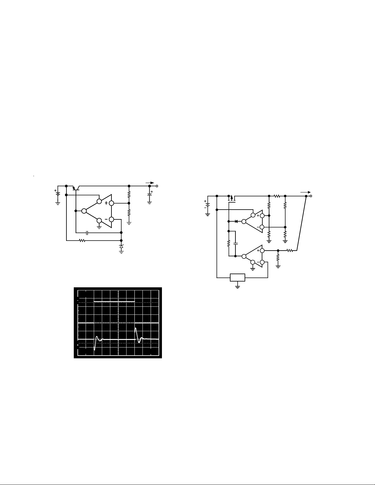
A 3 Volt Low-Dropout Linear Voltage Regulator
Figure 10 shows a simple 3 V voltage regulator design. The
regulator can deliver 50 mA load current while allowing a 0.2 V
dropout voltage. The OP295/OP495’s rail-to-rail output swing
handily drives the MJE350 pass transistor without requiring special drive circuitry. At no load, its output can swing less than the
pass transistor’s base-emitter voltage, turning the device nearly
off. At full load, and at low emitter-collector voltages, the transistor beta tends to decrease. The additional base current is easily handled by the OP295/OP495 output.
The amplifier servos the output to a constant voltage, which
feeds a portion of the signal to the error amplifier.
Higher output current, to 100 mA, is achievable at a higher
dropout voltage of 3.8 V.
< 50mA
I
1.235V
AD589
44.2k
1%
30.9k
1%
L
V
O
100µF
V
5V TO 3.2V
MJE 350
IN
43k
1
1000pF
8
1/2
OP295/
OP495
4
3
2
Figure 10. 3 V Low Dropout Voltage Regulator
Figure 11 shows the regulator’s recovery characteristic when its
output underwent a 20 mA to 50 mA step current change.
current limit loop. At this point A2’s lower output resistance
dominates the drive to the power MOSFET transistor, thereby
effectively removing the A1 voltage regulation loop from the
circuit.
If the output current greater than 1 amp persists, the current
limit loop forces a reduction of current to the load, which causes
a corresponding drop in output voltage. As the output voltage
drops, the current limit threshold also drops fractionally, resulting in a decreasing output current as the output voltage decreases, to the limit of less than 0.2 A at 1 V output. This
“fold-back” effect reduces the power dissipation considerably
during a short circuit condition, thus making the power supply
far more forgiving in terms of the thermal design requirements.
Small heat sinking on the power MOSFET can be tolerated.
The OP295’s rail-to-rail swing exacts higher gate drive to
the power MOSFET, providing a fuller enhancement to the
transistor. The regulator exhibits 0.2 V dropout at 500 mA of
load current. At 1 amp output, the dropout voltage is typically
5.6 volts.
R
SENSE
5
6
3
124k
2
0.1Ω
1/4W
210k1%205k
45.3k
1%
1%
2.500V
IRF9531
S
D
100k
5%
G
2
1N4148
OP295/
OP495
REF43
4
7
OP295/
OP495
0.01µF
1
1/2
8
A2
1/2
A1
4
6
6V
IO (NORM) = 0.5A
IO (MAX) = 1A
1%
45.3k
1%
124k
1%
+5V V
O
2V
100
50mA
20mA
OUTPUT
90
10
0%
20mV
1ms
STEP
CURRENT
CONTROL
WAVEFORM
Figure 11. Output Step Load Current Recovery
Low-Dropout, 500 mA Voltage Regulator with Fold-Back
Current Limiting
Adding a second amplifier in the regulation loop as shown in
Figure 12 provides an output current monitor as well as foldback current limiting protection.
Amplifier A1 provides error amplification for the normal voltage
regulation loop. As long as the output current is less than 1 ampere, amplifier A2’s output swings to ground, reverse biasing the
diode and effectively taking itself out of the circuit. However, as
the output current exceeds 1 amp, the voltage that develops
across the 0.1 Ω sense resistor forces the amplifier A2’s output
to go high, forward-biasing the diode, which in turn closes the
Figure 12. Low Dropout, 500 mA Voltage Regulator with
Fold-Back Current Limiting
Square Wave Oscillator
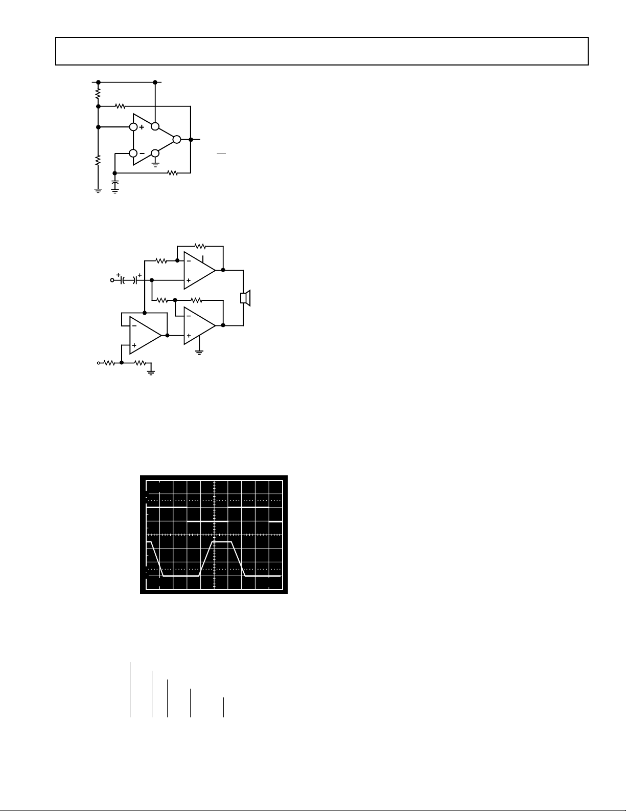
The circuit in Figure 13 is a square wave oscillator (note the
positive feedback). The rail-to-rail swing of the OP295/OP495
helps maintain a constant oscillation frequency even if the supply voltage varies considerably. Consider a battery powered system where the voltages are not regulated and drop over time.
The rail-to-rail swing ensures that the noninverting input sees
the full V+/2, rather than only a fraction of it.
The constant frequency comes from the fact that the 58.7 kΩ
feedback sets up Schmitt Trigger threshold levels that are directly proportional to the supply voltage, as are the RC charge
voltage levels. As a result, the RC charge time, and therefore the
frequency, remains constant independent of supply voltage. The
slew rate of the amplifier limits the oscillation frequency to a
maximum of about 800 Hz at a +5 V supply.
Single Supply Differential Speaker Driver
Connected as a differential speaker driver, the OP295/OP495
can deliver a minimum of 10 mA to the load. With a 600 Ω
load, the OP295/OP495 can swing close to 5 volts peak-to-peak
across the load.
–10–
REV. B
Page 11
OP295/OP495
V+
100k
100k
58.7k
1/2
OP295/
OP495
8
3
1
FREQ OUT
42
C
R
1
= < 350Hz @ V+ = +5V
f
OSC
RC
Figure 13. Square Wave Oscillator Has Stable Frequency
Regardless of Supply Changes
90.9k
V+
V
IN
1/4
OP295/
OP495
10k
2.2µF
10k 100k
20k20k
V+
1/4
OP295/
OP495
1/4
OP295/
OP495
SPEAKER
Figure 14. Single Supply Differential Speaker Driver
High Accuracy, Single-Supply, Low Power Comparator
The OP295/OP495 makes an accurate open-loop comparator.
With a single +5 V supply, the offset error is less than 300 µV. Fig-
ure 15 shows the OP295/OP495’s response time when operating
open-loop with 4 mV overdrive. It exhibits a 4 ms response time at
the rising edge and a 1.5 ms response time at the falling edge.
1V
100
90
INPUT
(5mV OVERDRIVE
@ OP295 INPUT)
OUTPUT
10
0%
5ms2V
Figure 15. Open-Loop Comparator Response Time with
5 mV Overdrive
OP295/OP495 SPICE MODEL Macro-Model
* Node Assignments
* Noninverting Input
* Inverting Input
* Positive Supply
* Negative Supply
* Output
*
*
.SUBCKT OP295 1 2 99 50 20
*
* INPUT STAGE
*
I1 99 4 2E-6
R1 1 6 5E3
R2 2 5 5E3
CIN 1 2 2E-12
IOS 1 2 0.5E-9
D1 5 3 DZ
D2 6 3 DZ
EOS 7 6 POLY (1) (31,39) 30E-6 0.024
Q1 8 5 4 QP
Q2974QP
R3 8 50 25.8E3
R4 9 50 25.8E3
*
* GAIN STAGE
*
R7 10 98 270E6
G1 98 10 POLY (1)(9,8) –4.26712E-9 27.8E-6
EREF 98 0 (39, 0) 1
R5 99 39 100E3
R6 39 50 100E3
*
* COMMON MODE STAGE
*
ECM 30 98 POLY(2) (1,39) (2,39) 0 0.5 0.5
R12 30 31 1E6
R13 31 98 100
*
* OUTPUT STAGE
*
I2 18 50 1.59E-6
V2 99 12 DC 2.2763
Q4 10 14 50 QNA 1.0
R11 14 50 33
M3 15 10 13 13 MN L=9E-6 W=102E-6 AD=15E-10 AD=15E-10
M4 13 10 50 50 MN L=9E-6 W=50E-6 AD=75E-11 AS=75E-11
D8 10 22 DX
V3 22 50 DC 6
M2 20 10 14 14 MN L=9E-6 W=2000E-6 AD=30E-9 AS=30E-9
Q5 17 17 99 QPA 1.0
Q6 18 17 99 QPA 4.0
R8 18 99 2.2E6
Q7 18 19 99 QPA 1.0
R9 99 19 8
C2 18 99 20E-12
M6 15 12 17 99 MP L=9E-6 W=27E-6 AD=405E-12 AS=405 E-12
M1 20 18 19 99 MP L=9E-6 W=2000E-6 AD=30E-9 AS=30E-9
D4 21 18 DX
V4 99 21 DC 6
R10 10 11 6E3
C3 11 20 50E-12
.MODEL QNA NPN (IS=1.19E-16 BF=253 NF=0.99 VAF=193 IKF=2.76E-3
+ ISE=2.57E-13 NE=5 BR=0.4 NR=0.988 VAR=15 IKR=1.465E-4
+ ISC=6.9E-16 NC=0.99 RB=2.0E3 IRB=7.73E-6 RBM=132.8 RE=4
RC=209
+ CJE=2.1E-13 VJE=0.573 MJE=0.364 FC=0.5 CJC=1.64E-13 VJC=0.534
MJC=0.5
+ CJS=1.37E-12 VJS=0.59 MJS=0.5 TF=0.43E-9 PTF=30)
.MODEL QPA PNP (IS=5.21E-17 BF=131 NF=0.99 VAF=62 IKF=8.35E-4
+ ISE=1.09E-14 NE=2.61 BR=0.5 NR=0.984 VAR=15 IKR=3.96E-5
+ ISC=7.58E-16 NC=0.985 RB=1.52E3 IRB=1.67E-5 RBM=368.5 RE=6.31
RC=354.4
+ CJE=1.1E-13 VJE=0.745 MJE=0.33 FC=0.5 CJC=2.37E-13 VJC=0.762
MJC=0.4
+ CJS =7.11E-13 VJS=0.45 MJS=0.412 TF=1.0E-9 PTF=30)
.MODEL MN NMOS (LEVEL=3 VTO=1.3 RS=0.3 RD=0.3
+ TOX=8.5E-8 LD=1.48E-6 NSUB=1.53E16 UO=650 DELTA=10 VMAX=2E5
+ XJ=1.75E-6 KAPPA=0.8 ETA=0.066 THETA=0.01 TPG=1 CJ=2.9E-4
PB=0.837
+ MJ=0.407 CJSW=0.5E-9 MJSW=0.33)
.MODEL MP PMOS (LEVEL=3 VTO=–1.1 RS=0.7 RD=0.7
+ TOX=9.5E-8 LD=1.4E-6 NSUB=2.4E15 UO=650 DELTA=5.6 VMAX=1E5
+ XJ=1.75E-6 KAPPA=1.7 ETA=0.71 THETA=5.9E-3 TPG=–1 CJ=1.55E-4
PB=0.56
+ MJ=0.442 CJSW=0.4E-9 MJSW=0.33)
.MODEL DX D(IS=1E-15)
.MODEL DZ D (IS=1E-15, BV=7)
.MODEL QP PNP (BF=125)
.ENDS
REV. B
–11–
Page 12
OP295/OP495
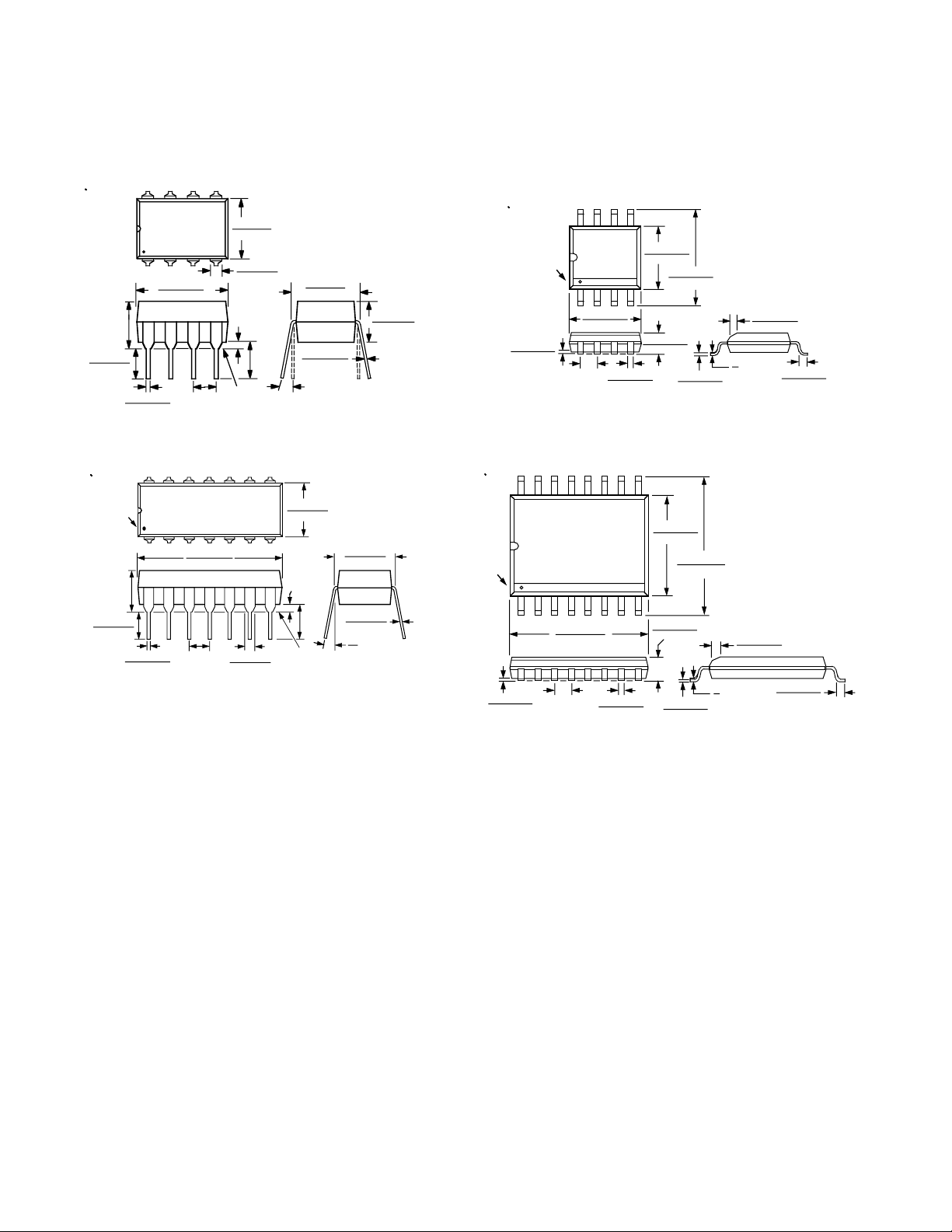
OUTLINE DIMENSIONS
Dimensions shown in inches and (mm)
0.210
(5.33)
MAX
0.160 (4.06)
0.115 (2.93)
PIN 1
0.210
(5.33)
MAX
0.160 (4.06)
0.115 (2.92)
8 Lead Plastic DIP (P Suffix)
8
1
0.022 (0.558)
0.014 (0.356)
0.430 (10.92)
0.348 (8.84)
0.100
(2.54)
BSC
5
4
0.280 (7.11)
0.240 (6.10)
0.070 (1.77)
0.045 (1.15)
0.015
(0.381) TYP
SEATING
PLANE
0.130
(3.30)
MIN
0°- 15°
14-Lead Plastic DIP (P Suffix)
14
1
0.022 (0.558)
0.014 (0.36)
0.795 (20.19)
0.725 (18.42)
0.100
(2.54)
BSC
0.070 (1.77)
0.045 (1.15)
8
7
0.325 (8.25)
0.300 (7.62)
0.015 (0.381)
0.008 (0.204)
0.280 (7.11)
0.240 (6.10)
0.015
(0.381)
MIN
0.130
(3.30)
MIN
SEATING
PLANE
0.325 (8.25)
0.300 (7.62)
0.015 (0.38)
0.008 (0.20)
15°
0°
0.195 (4.95)
0.115 (2.93)
0.0098 (0.25)
0.0040 (0.10)
16
PIN 1
0.0118 (0.30)
0.0040 (0.10)
8-Lead Narrow-Body SO (S Suffix)
0.1968 (5.00)
0.1890 (4.80)
0.0192 (0.49)
0.0138 (0.35)
5
4
0.0688 (1.75)
0.0532 (1.35)
0.1574 (4.00)
0.1497 (3.80)
0.2440 (6.20)
0.2284 (5.80)
0.0098 (0.25)
0.0075 (0.19)
PIN 1
8
1
0.0500
(1.27)
BSC
16-Lead Wide-Body SO (S Suffix)
9
0.2992 (7.60)
0.2914 (7.40)
0.4193 (10.65)
0.3937 (10.00)
0.0192 (0.49)
0.0138 (0.35)
8
0.1043 (2.65)
0.0926 (2.35)
0.0125 (0.32)
0.0091 (0.23)
1
0.4133 (10.50)
0.3977 (10.10)
0.0500 (1.27)
BSC
8
°
0
°
0.0196 (0.50)
0.0099 (0.25)
8
°
0
°
0.0291 (0.74)
0.0098 (0.25)
x 45
0.0500 (1.27)
0.0160 (0.41)
x 45
°
0.0500 (1.27)
0.0157 (0.40)
°
C1806a–10–7/95
–12–
PRINTED IN U.S.A.
REV. B
 Loading...