

Page 1
Precision Rail-to-Rail Input & Output
1
2
3
45
6
7
8
OUT A
–IN A
+IN A
V–
OP-482
V+
OUT B
–IN B
+IN B
OP284
a
FEATURES
Single-Supply Operation
Wide Bandwidth: 4 MHz
Low Offset Voltage: 65 mV
Unity-Gain Stable
High Slew Rate: 4.0 V/ms
Low Noise: 3.9 nV/√
APPLICATIONS
Battery Powered Instrumentation
Power Supply Control and Protection
Telecom
DAC Output Amplifier
ADC Input Buffer
GENERAL DESCRIPTION
The OP184/OP184/OP284/OP484 are single, dual and quad
single-supply, 4 MHz bandwidth amplifiers featuring rail-to-rail
inputs and outputs. They are guaranteed to operate from +3 to
+36 (or ±1.5 to ±18) volts and will function with a single supply
as low as +1.5 volts.
These amplifiers are superb for single supply applications requiring both ac and precision dc performance. The combination
of bandwidth, low noise and precision makes the OP184/OP284/
OP484 useful in a wide variety of applications, including filters
and instrumentation.
Other applications for these amplifiers include portable telecom
equipment, power supply control and protection, and as amplifiers or buffers for transducers with wide output ranges. Sensors
requiring a rail-to-rail input amplifier include Hall effect, piezo
electric, and resistive transducers.
The ability to swing rail-to-rail at both the input and output enables designers to build multistage filters in single-supply systems and maintain high signal-to-noise ratios.
The OP184/OP284/OP484 are specified over the HOT extended
industrial (–40°C to +125°C) temperature range. The single
and dual are available in 8-pin plastic DIP plus SO surface
mount packages. The quad OP484 is available in 14-pin plastic
DIPs and 14-lead narrow-body SO packages.
Hz
Operational Amplifiers
OP184/OP284/OP484
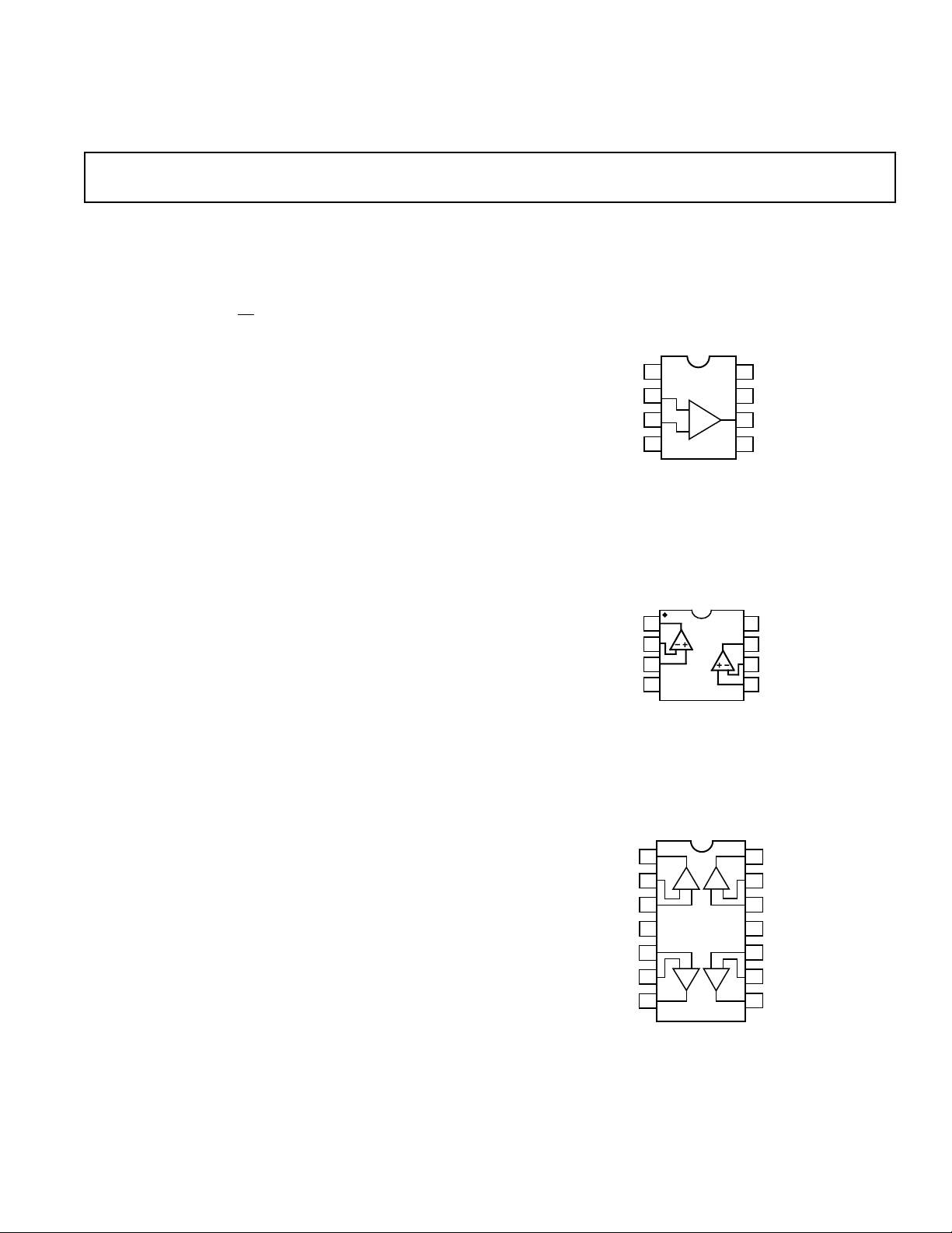
PIN CONFIGURATIONS
8-Lead Epoxy DIP
(P Suffix)
8-Lead SO
(S Suffix)
NULL
1
OP184
2
–IN A
+IN A
V–
–
3
+
4
NC = NO CONNECT
8-Lead Epoxy DIP
(P Suffix)
8-Lead SO
(S Suffix)
14-Lead Epoxy DIP
(P Suffix)
14-Lead Narrow-Body SO
(S Suffix)
OUT A
1
2
–IN A
+IN A
V+
+IN B
–IN B
OUT B
–+
3
4
OP484
5
–+
6
7
NC
8
V+
7
OUT A
6
NULL
5
OUT D
14
13
–
–+
–IN D
12
+IN D
11
V–
+IN C
10
–IN C
9
8
OUT C
+
REV. 0
Information furnished by Analog Devices is believed to be accurate and
reliable. However, no responsibility is assumed by Analog Devices for its
use, nor for any infringements of patents or other rights of third parties
which may result from its use. No license is granted by implication or
otherwise under any patent or patent rights of Analog Devices.
© Analog Devices, Inc., 1996
One Technology Way, P.O. Box 9106, Norwood. MA 02062-9106, U.S.A.
Tel: 617/329-4700 Fax: 617/326-8703
Page 2

OP184/OP284/OP484–SPECIFICA TIONS
ELECTRICAL CHARACTERISTICS
(@ VS = +5.0 V, VCM = 2.5 V, TA = +258C unless otherwise noted)
Parameter Symbol Conditions Min Typ Max Units
INPUT CHARACTERISTICS
Offset Voltage “OP184/284E” Grade V
Offset Voltage “OP184/284F” Grade V
Offset Voltage OP184 “484E” Grade V
Offset Voltage OP184 “484F” Grade V
Input Bias Current I
Input Offset Current I
OS
OS
OS
OS
B
OS
(Note 1) 65 µV
–40°C ≤ T
≤ +125°C 165 µV
A
125 µV
–40°C ≤ T
≤ +125°C 350 µV
A
75 µV
–40°C ≤ T
≤ +125°C 175 µV
A
150 µV
–40°C ≤ T
≤ +125°C 450 µV
A
60 300 nA
–40°C ≤ T
≤ +125°C 500 nA
A
250nA
–40°C ≤ T
≤ +125°C50nA
A
Input Voltage Range 0+5V
Common-Mode Rejection Ratio CMRR V
Common-Mode Rejection Ratio CMRR V
Large Signal Voltage Gain A
VO
= 0 V to 5 V 60 dB
CM
= 1.0 V to 4.0 V, –40°C ≤ TA ≤ +125°C86 dB
CM
RL = 2 kΩ, 1 V ≤ VO ≤ 4 V 50 240 V/mV
R
= 2 kΩ, –40°C ≤ TA ≤ +125°C 25 V/mV
L
Bias Current Drift ∆IB/∆T 150 pA/°C
OUTPUT CHARACTERISTICS
Output Voltage High V
Output Voltage Low V
Output Currrent I
OH
OL
OUT
IL = 1.0 mA +4.85 V
IL = 1.0 mA 125 mV
± 6.5 mA
POWER SUPPLY
Power Supply Rejection Ratio PSRR V
Supply Current/Amplifier I
Supply Voltage Range V
SY
S
= +2.0 V to +10 V, –40°C ≤ TA ≤ +125°C76 dB
S
VO = 2.5 V, –40°C ≤ TA ≤ +125°C 1.25 mA
+3 +36 V
DYNAMIC PERFORMANCE
Slew Rate SR R
Settling Time t
s
= 2 kΩ 1.65 2.4 V/µs
L
To 0.01%, 1.0 V Step 2.5 µs
Gain Bandwidth Product GBP 3.25 MHz
Phase Margin Øo 45 Degrees
NOISE PERFORMANCE
Voltage Noise e
Voltage Noise Density e
Current Noise Density i
NOTES
1
Input Offset Voltage measurements are performed by automated test equipment approximately 0.5 seconds after application of power.
Specifications subject to change without notice.
p-p 0.1 Hz to 10 Hz 0.3 µV p-p
n
n
n
f = 1 kHz 3.9 nV/√Hz
0.4 pA/√Hz
–2–
REV. 0
Page 3

OP184/OP284/OP484
ELECTRICAL CHARACTERISTICS
(@ VS = +3.0 V, VCM = 1.5 V, TA = +258C unless otherwise noted)
Parameter Symbol Conditions Min Typ Max Units
INPUT CHARACTERISTICS
Offset Voltage “OP184/284E” Grade V
Offset Voltage “OP184/284F” Grade V
Offset Voltage OP184“484E” Grade V
Offset Voltage OP184“484F” Grade V
Input Bias Current I
Input Offset Current I
OS
OS
OS
OS
B
OS
(Note 1) 65 µV
–40°C ≤ T
≤ +125°C 165 µV
A
125 µV
–40°C ≤ T
≤ +125°C 350 µV
A
100 µV
–40°C ≤ T
≤ +125°C 200 µV
A
150 µV
–40°C ≤ T
≤ +125°C 450 µV
A
60 300 nA
–40°C ≤ T
≤ +125°C 500 nA
A
–40°C ≤ TA ≤ +125°C50nA
Input Voltage Range 0+3V
Common-Mode Rejection Ratio CMRR V
= 0 V to 3 V 60 dB
CM
Common-Mode Rejection Ratio CMRR VCM = 0 V to 3 V, –40°C ≤ TA ≤ +125°C56 dB
OUTPUT CHARACTERISTICS
Output Voltage High V
Output Voltage Low V
OH
OL
IL = 1.0 mA +2.85 V
IL = 1.0 mA 125 mV
POWER SUPPLY
Power Supply Rejection Ratio PSRR V
Supply Current/Amplifier I
SY
= ±1.25 V to ±1.75 V 76 dB
S
VO = 1.5 V, –40°C ≤ TA ≤ +125°C 1.15 mA
DYNAMIC PERFORMANCE
Gain Bandwidth Product GBP 3 MHz
NOISE PERFORMANCE
Voltage Noise Density e
NOTES
1
Input Offset Voltage measurements are performed by automated test equipment approximately 0.5 seconds after application of power.
Specifications subject to change without notice.
n
f = 1 kHz 3.9 nV/√Hz
REV. 0
–3–
Page 4

OP184/OP284/OP484
ELECTRICAL CHARACTERISTICS
(@ VS = 615.0 V, VCM = 0 V, TA = +258C unless otherwise noted)
Parameter Symbol Conditions Min Typ Max Units
INPUT CHARACTERISTICS
Offset Voltage “OP184/284E” Grade V
Offset Voltage “284F” Grade V
Offset Voltage “484E” Grade V
Offset Voltage “484F” Grade V
Input Bias Current I
Input Offset Current I
OS
OS
OS
OS
B
OS
(Note 1) 100 µV
–40°C ≤ T
≤ +125°C 200 µV
A
175 µV
–40°C ≤ T
≤ +125°C 375 µV
A
150 µV
–40°C ≤ T
≤ +125°C 300 µV
A
250 µV
–40°C ≤ T
≤ +125°C 500 µV
A
80 300 nA
–40°C ≤ T
≤ +125°C 500 nA
A
–40°C ≤ TA ≤ +125°C50nA
Input Voltage Range –15 +15 V
Common-Mode Rejection Ratio CMRR V
Common-Mode Rejection Ratio CMRR V
Large Signal Voltage Gain A
Offset Voltage Drift “E” Grade ∆ V
VO
/∆T 0.2 2.00 µV/°C
OS
= –14.0 V to +14.0 V, –40°C ≤ TA ≤ +125°C86 90 dB
CM
= –15.0 V to +15.0 V 80 dB
CM
RL = 2 kΩ, –10 V ≤ VO ≤ 10 V 150 1000 V/mV
= 2 kΩ, –40°C ≤ TA ≤ +125°C 75 V/mV
R
L
Bias Current Drift ∆IB/∆T 150 pA/°C
OUTPUT CHARACTERISTICS
Output Voltage High V
Output Voltage Low V
Output Current I
OH
OL
OUT
IL = 1.0 mA +14.8 V
IL = 1.0 mA –14.875 V
±10 mA
POWER SUPPLY
Power Supply Rejection Ratio PSRR V
Supply Current/Amplifier I
Supply Current/Amplifier I
SY
SY
= ±2.0 V to ±18 V, –40°C ≤ TA ≤ +125°C90 dB
S
VO = 0 V, –40°C ≤ TA ≤ +125°C 1.75 mA
VS = ± 18 V, –40°C ≤ TA ≤ +125°C 2.0 mA
DYNAMIC PERFORMANCE
Slew Rate SR R
Full-Power Bandwidth BW
Settling Time t
p
S
= 2 kΩ 2.4 4.0 V/µs
L
1% Distortion, RL = 2 kΩ, VO = 29 V p-p 35 kHz
To 0.01%, 10 V Step 4 µs
Gain Bandwidth Product GBP 4.25 MHz
Phase Margin Øo 50 Degrees
NOISE PERFORMANCE
Voltage Noise e
Voltage Noise Density e
Current Noise Density i
NOTES
1
Input Offset Voltage measurements are performed by automated test equipment approximately 0.5 seconds after application of power.
Specifications subject to change without notice.
p-p 0.1 Hz to 10 Hz 0.3 µV p-p
n
n
n
f = 1 kHz 3.9 nV/√Hz
0.4 pA/√Hz
W AFER TEST LIMITS
(@ VS = +5.0 V, VCM = 2.5 V, TA = +258C unless otherwise noted)
Parameter Symbol Conditions Limit Units
Offset Voltage OP284 V
Offset Voltage OP484 V
Input Bias Current I
Input Offset Current I
Input Voltage Range V
Common-Mode Rejection Ratio CMRR V
Power Supply Rejection Ratio PSRR V
Large Signal Voltage Gain A
Output Voltage High V
Output Voltage Low V
Supply Current/Amplifier I
NOTE
Electrical tests and wafer probe to the limits shown. Due to variations in assembly methods and normal yield loss, yield after packaging is not guaranteed for standard
product dice. Consult factory to negotiate specifications based on dice lot qualifications through sample lot assembly and testing.
B
OS
SY
OS
OS
CM
VO
OH
OL
= +1 V to +4 V 86 dB min
CM
= ±2 V to ±18 V 90 dB min
S
RL = 2 kΩ 50 V/mV min
IL = 1.0 mA 4.85 V min
IL = 1.0 mA 125 mV max
VO = 0 V, RL = ∞ 1.25 mA max
–4–
65 µV max
75 µV max
300 nA max
50 nA max
V– to V+ V min
REV. 0
Page 5
OP184/OP284/OP484
ABSOLUTE MAXIMUM RATINGS
1
Supply Voltage . . . . . . . . . . . . . . . . . . . . . . . . . . . . . . . . .±18 V
Input Voltage . . . . . . . . . . . . . . . . . . . . . . . . . . . . . . . . . .±18 V
Differential Input Voltage
Output Short-Circuit Duration to GND
2
. . . . . . . . . . . . . . . . . . . . . . ±0.6 V
3
. . . . . . . . .Indefinite
Storage Temperature Range
P, S Packages . . . . . . . . . . . . . . . . . . . . . . .–65°C to +150°C
Operating Temperature Range
OP184/OP284/OP484E, F . . . . . . . . . . . . .–40°C to +125°C
Junction Temperature Range
P, S Packages . . . . . . . . . . . . . . . . . . . . . . .–65°C to +150°C
Lead Temperature Range (Soldering 60 sec) . . . . . . . . +300°C
Package Type θ
3
JA
θ
JC
Units
8-Pin Plastic DIP (P) 103 43 °C/W
8-Pin SOIC (S) 158 43 °C/W
14-Pin Plastic DIP (P) 83 39 °C/W
14-Pin SOIC (S) 92 27 °C/W
NOTES
1
Absolute maximum ratings apply to both DICE and packaged parts, unless
otherwise noted.
2
For input voltages greater than 0.6 volts the input current should be limited to less
than 5 mA to prevent degradation or destruction of the input devices.
3
θJA is specified for the worst case conditions; i.e., θ
for cerdip, and P-DIP packages, θ
for SOIC package.
is specified for device soldered in circuit board
JA
is specified for device in socket
JA
OP284 Die Size 0.065 × 0.092 Inch, 5,980 Sq. Mils
Substrate (Die Backside) Is Connected to V–.
Transistor Count, 62.
ORDERING GUIDE
Temperature Package Package
Model Range Description Option
OP184EP –40°C to +125°C 8-Pin Plastic DIP N-8
OP184ES –40 °C to +125°C 8-Pin SOIC SO-8
OP184FP –40°C to +125°C 8-Pin Plastic DIP N-8
OP184FS –40°C to +125°C 8-Pin SOIC SO-8
OP284EP –40°C to +125°C 8-Pin Plastic DIP N-8
OP284ES –40 °C to +125°C 8-Pin SOIC SO-8
OP284FP –40°C to +125°C 8-Pin Plastic DIP N-8
OP284FS –40°C to +125°C 8-Pin SOIC SO-8
OP484EP –40°C to +125°C 14-Pin Plastic DIP N-14
OP484ES –40 °C to +125°C 14-Pin SOIC SO-14
OP484FP –40°C to +125°C 14-Pin Plastic DIP N-14
OP484FS –40°C to +125°C 14-Pin SOIC SO-14
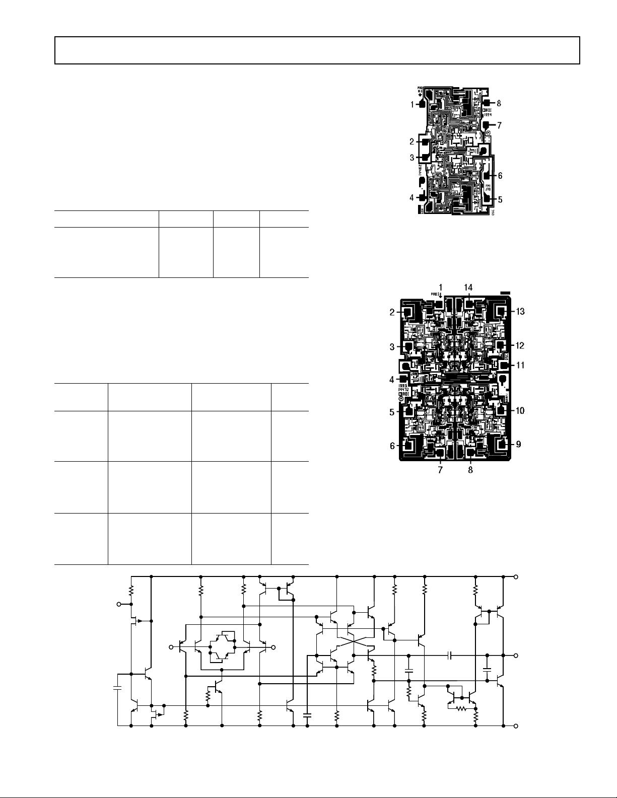
QB5QB6
Q2
QB4
R2
TP
CB1 N+
JB1
P+M
QB1
RB1
–IN +IN
QB2
JB2
R3
Q3
Q1
RB2
R1
R4
QL1
QL2
QB3
Q4
Q7
Q5
CC1
OP484 Die Size 0.080 × 0.110 Inch, 8,800 Sq. Mils
Substrate (Die Backside) Is Connected to V–.
Transistor Count, 120.
V
CC
CFF
QB10
Q13
RB4
R8
Q14
CC2
R11
Q17Q16
Q18
OUT
V
EE
O
C
Q15
R9
R10
Q11
Q9
RB3
Q12
Q8
Q6
QB7
R5
QB9
Q10
R6
R7
QB8
REV. 0
Figure 1. Simplified Schematic
–5–
Page 6
COMMON MODE VOLTAGE – Volts
INPUT BIAS CURRENT – nA
500
–500
–15 –10 15–5 5 100
400
300
200
100
0
–100
–200
–300
–400
VS = ±15V
LOAD CURRENT – mA
OUTPUT VOLTAGE – mV
1,000
100
10
0.01 0.1 10
1
SOURCE
SINK
VS = ±15V
TEMPERATURE – °C
SUPPLY CURRENT/AMPLIFIER – mA
1.2
0.5
1.1
0.8
0.7
0.6
1.0
0.9
–40 12525 85
VS = ±15V
VS = +5V
VS = +3V
OP184/OP284/OP484–T ypical Performance Characteristics
300
VS = +3V
270
= +25°C
T
A
240
VCM = 1.5V
210
180
150
120
QUANTITY
90
60
30
0
–100 –75 100
–50 –25 0 25 50 75
INPUT OFFSET VOLTAGE – µV
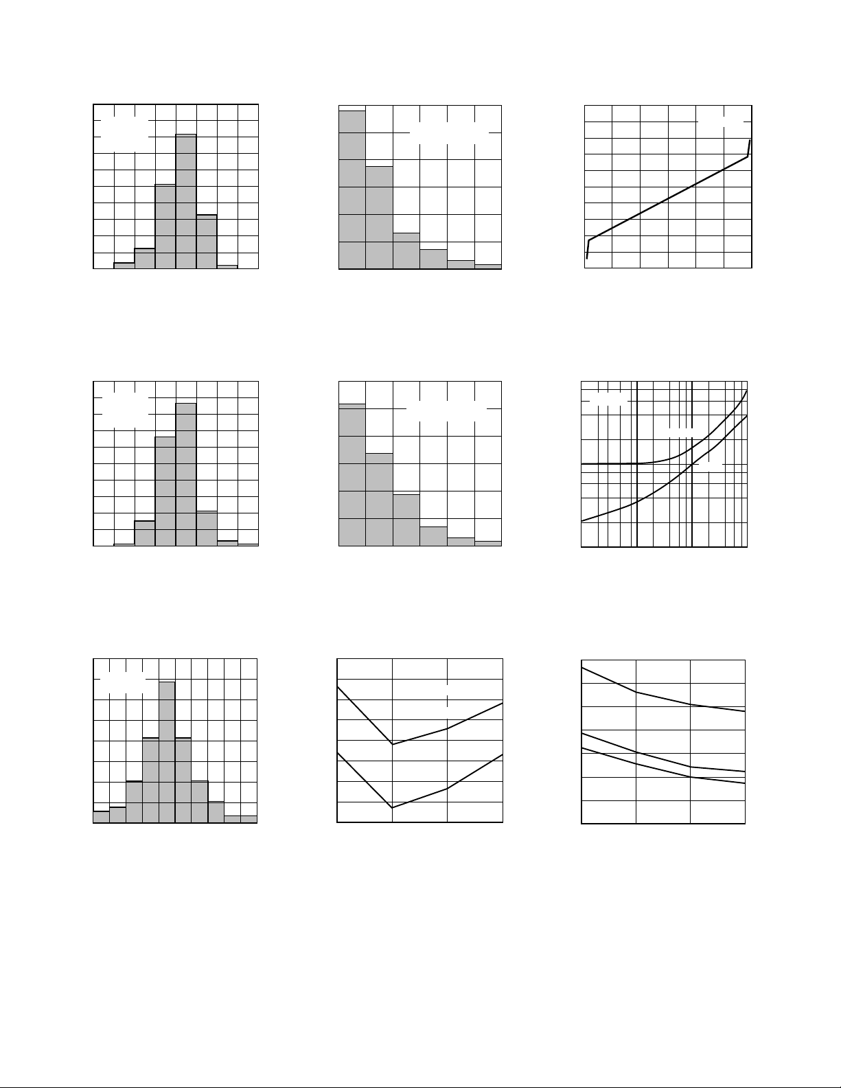
Figure 2. Input Offset Voltage
Distribution
300
VS = +5V
270
TA = +25°C
240
VCM = 2.5V
210
180
150
120
QUANTITY
90
60
30
0
–100 –75 100
–50 –25 0 25 50 75
INPUT OFFSET VOLTAGE – µV
300
250
200
150
QUANTITY
100
50
0
0 0.25 1.50.50 0.75 1.0 1.25
OFFSET VOLTAGE DRIFT, TCVOS – µV/°C
VS = +5V
–40°C ≤ T
≤ +125°C
A
Figure 5. Input Offset Voltage Drift
Distribution
300
250
200
150
QUANTITY
100
50
0
0 0.25 1.50.50 0.75 1.0 1.25
OFFSET VOLTAGE DRIFT, TCVOS – µV/°C
VS = ±15V
–40°C ≤ T
≤ +125°C
A
Figure 8. Input Bias Current vs.
Common-Mode Voltage
Figure 3. Input Offset Voltage
Distribution
200
VS = ±15V
175
T
= +25°C
A
150
125
100
QUANTITY
75
50
25
0
–75 –50 0 50 75 100
–125 –100 125
–25 25
INPUT OFFSET VOLTAGE – µV
Figure 4. Input Offset Voltage
Distribution
Figure 6. Input Offset Voltage Drift
Distribution
–40
–45
–50
–55
–60
–65
–70
INPUT BIAS CURRENT – nA
–75
–80
–40 12525 85
TEMPERATURE – °C
VCM = VS/2
VS = +5V
VS = ±15V
Figure 7. Bias Current vs.
Temperature
–6–
Figure 9. Output Voltage to Supply
Rail vs. Load Current
Figure 10. Supply Current vs.
Temperature
REV. 0
Page 7

OP184/OP284/OP484
FREQUENCY – Hz
30
10
CLOSED-LOOP GAIN – dB
40
60
10
–40
100 10k
1M 10M
–10
VS = +5V
R
L
= 2kΩ
T
A
= +25°C
–20
–30
0
20
50
1k
100k
FREQUENCY – Hz
30
10
CLOSED-LOOP GAIN – dB
40
60
10
–40
100 10k
1M 10M
–10
VS = ±15V
R
L
= 2kΩ
T
A
= +25°C
–20
–30
0
20
50
1k
100k
FREQUENCY – Hz
30
10
CLOSED-LOOP GAIN – dB
40
60
10
–40
100 10k
1M 10M
–10
VS = +3V
R
L
= 2kΩ
T
A
= +25°C
–20
–30
0
20
50
1k
100k
1.50
1.25
1.0
0.75
0.5
0.25
SUPPLY CURRENT (PER AMPLIFIER) – mA
0
0 ±2.5 ±20±5.0 ±10 ±12.5 ±15
SUPPLY VOLTAGE – Volts
TA = +25°C
±17.5±7.5
Figure 11. Supply Current vs. Supply
Voltage
50
–I
SC
VS = ±15V
+I
SC
40
30
20
10
SHORT CIRCUIT CURRENT – mA
0
–50 125
–I
SC
+I
SC
VS = +5V, VCM = +2.5V
–25 0 25 7550 100
TEMPERATURE – °C
80
60
50
40
30
20
10
0
OPEN-LOOP GAIN – dB
–10
–20
–30
10k 100k 10M
FREQUENCY – Hz
VS = +3V
T
A
NO LOAD
1M
= +25°C
0
45
90
135
180
225
270
Figure 14. Open-Loop Gain and Phase
vs. Frequency (No Load)
80
60
50
40
30
20
10
0
OPEN-LOOP GAIN – dB
–10
–20
–30
10k 100k 10M
FREQUENCY – Hz
VS = ±15V
T
A
NO LOAD
1M
= +25°C
0
45
90
135
180
225
270
PHASE SHIFT – Degrees
Figure 17. Closed-Loop Gain vs.
Frequency (2 k
PHASE SHIFT – Degrees
Ω
Load)
Figure 12. Short Circuit Current vs.
Temperature
80
60
50
40
30
20
10
0
OPEN-LOOP GAIN – dB
–10
–20
–30
10k 100k 10M
Figure 13. Open-Loop Gain and Phase
vs. Frequency (No Load)
REV. 0
FREQUENCY – Hz
VS = +5V
T
A
NO LOAD
1M
= +25°C
Figure 15. Open-Loop Gain and Phase
vs. Frequency (No Load)
2.5k
2k
0
45
90
135
180
225
PHASE SHIFT – Degrees
270
1.5k
1k
OPEN-LOOP GAIN – V/mV
500
0
–25 0 25 7550 100
–50 125
VS = ±15V
–10V < V
R
= 2kΩ
L
VS = +5V
1V < V
< 4V
O
R
= 2kΩ
L
TEMPERATURE – °C
Figure 16. Open-Loop Gain vs.
Temperature
–7–
< 10V
O
Figure 18. Closed-Loop Gain vs.
Ω
Frequency (2 k
Load)
Figure 19. Closed-Loop Gain vs.
Ω
Frequency (2 k
Load)
Page 8

FREQUENCY – Hz
100
100
PSRR – dB
120
160
60
–40
1k 100k
10M
20
TA = +25°C
0
–20
40
80
140
10k 1M
VS = ±15V
VS = +5V
VS = +3V
CAPACITIVE LOAD – pF
OVERSHOOT – %
80
70
0
10 100 1000
60
50
40
30
20
10
–OS
+OS
VS = ±2.5V
T
A
= +25°C, A
VCL
= 1
V
IN
= ±50mV
OP184/OP284/OP484–T ypical Performance Characteristics
300
VS = +5V
270
T
= +25°C
A
240
210
180
150
120
90
OUTPUT IMPEDANCE – Ω
60
30
0
100
AV = 100
10k 1M
1k 100k
FREQUENCY – Hz
AV = 10
AV = 1
Figure 20. Output Impedance vs.
Frequency
300
VS = ±15V
270
T
= +25°C
A
240
210
180
150
120
90
OUTPUT IMPEDANCE – Ω
60
30
0
1k 100k
100
AV = 100
10k 1M
FREQUENCY – Hz
AV = 10
AV = 1
10M
10M
5
4
3
2
VS = +5V
V
= 0.5–4.5V
IN
1
R
= 2kΩ
L
T
MAXIMUM OUTPUT SWING – Vp-p
= +25°C
A
0
1k
10k 100k 1M 10M
FREQUENCY – Hz
Figure 23. Maximum Output Swing
vs. Frequency
30
25
20
15
10
5
MAXIMUM OUTPUT SWING – Vp-p
0
10k 100k 1M 10M
1k
FREQUENCY – Hz
VS = ±15V
= ±14V
V
IN
= 2kΩ
R
L
= +25°C
T
A
Figure 26. PSRR vs. Frequency
Figure 21. Output Impedance vs.
Frequency
300
VS = +3V
270
T
= +25°C
A
240
210
180
150
120
90
OUTPUT IMPEDANCE – Ω
60
30
0
100
1k 100k
AV = 100
10k 1M
FREQUENCY – Hz
Figure 22. Output Impedance vs.
Frequency
AV = 10
AV = 1
10M
Figure 24. Maximum Output Swing
vs. Frequency
180
TA = +25°C
160
140
120
100
80
60
CMRR – dB
40
20
0
–20
100
10k 1M
1k 100k
FREQUENCY – Hz
VS = ±15V
VS = +3V
VS = +5V
10M
Figure 25. CMRR vs. Frequency
–8–
Figure 27. Small Signal Overshoot
vs. Capacitive Load
7
6
+SLEW RATE
5
–SLEW RATE
4
3
+SLEW RATE
SLEW RATE – V/µs
2
–SLEW RATE
1
0
–50 125
–25 0 75 100
25 50
TEMPERATURE – °C
VS = ±15V
R
= 2kΩ
L
VS = +5V
R
= 2kΩ
L
Figure 28. Slew Rate vs.Temperature
REV. 0
Page 9

OP184/OP284/OP484
10
0%
100
90
1s
10mV
VS = ±15V
A
V
= 100k
e
n
= 0.3µVp-p
FREQUENCY – Hz
100
100
120
160
60
–40
1k 100k 10M
20
0
–20
40
80
140
10k 1M
VS = ±15V
VS = +3V
TA = +25°C
CHANNEL SEPARATION – dB
10
0%
100
90
1µs
100mV
VS = +5V
A
V
= 1
R
L
= 2kΩ
C
L
= 300pF
T
A
- +25°C
400mV
0V
30
25
Hz
√
20
15
10
NOISE DENSITY – nV/
5
0
1
FREQUENCY – Hz
±2.5V ≤ VS ≤ ±15V
T
= +25°C
A
10010
1000
Figure 29. Voltage Noise Density
vs. Frequency
10
±2.5V ≤ VS ≤ ±15V
T
= +25°C
8
6
4
2
CURRENT NOISE DENSITY – pA/√Hz
0
1
A
FREQUENCY – Hz
10010
1000
10
8
6
4
2
0
0.1%
–2
–4
STEP SIZE – Volts
–6
–8
–10
01 624
0.01%
SETTLING TIME – µs
VS = ±15V
T
= +25°C
A
53
Figure 32. Settling Time vs. Step Size
Figure 35. Channel Separation
vs. Frequency
100
90
+400mV
10
0V
0%
100mV
VS = +5V
A
= 1
V
= OPEN
R
L
= 300pF
C
L
= +25°C
T
A
1µs
Figure 30. Current Noise Density
vs. Frequency
Figure 31. Settling Time vs. Step Size
REV. 0
5
4
3
2
1
0.1% 0.01%
0
–1
STEP SIZE – Volts
–2
–3
–4
–5
01 624
SETTLING TIME – µs
VS = +5V
T
= +25°C
A
53
Figure 33. 0.1 Hz to 10 Hz Noise
VS = +5V, 0V
A
100
e
90
10
0%
= 100k
V
= 0.3µVp-p
n
10mV
1s
Figure 34. 0.1 Hz to 10 Hz Noise
–9–
Figure 36. Small Signal Transient
Response
Figure 37. Small Signal Transient
Response
Page 10

OP184/OP284/OP484
V
POS
I2
I1
Q1
Q3
Q4
Q2
V
NEG
Q5
V
OUT
Q6
R6
R3
R2
R1
R4
INPUT FROM
SECOND GAIN
STAGE
R5
D1
0.1
VS = ±1.5V
A
200mV
–200mV
100
90
0V
10
0%
100mV
V
NO LOAD
T
= +25°C
A
500ns
Figure 38. Small Signal Transient
Response
= 1
200mV
–200mV
VS = ±0.75V
= 1
A
V
100
NO LOAD
90
T
= +25°C
A
0V
10
0%
100mV
Figure 39. Small Signal Transient
Response
APPLICATIONS
Functional Description
The OP284 and OP484 are precision single-supply, rail-to-rail
operational amplifiers. Intended for the portable instrumentation marketplace, the OP184/OP284/OP484 combines the attributes of precision, wide bandwidth, and low noise to make it
a superb choice in those single supply applications that require
both ac and precision dc performance. Other low supply voltage
applications for which the OP284 is well suited are active filters,
audio microphone preamplifiers, power supply control, and telecom. To combine all of these attributes with rail-to-rail input/
output operation, novel circuit design techniques are used.
V
POS
+IN
R1
4k
Q3Q1 Q2
R3
3k
D1
D2
I1
Q4
I2
R2
4k
V
01
–IN
V
R4
3k
02
VO = ±0.75V
AV = 1000
= ±2.5V
V
S
= 2kΩ
R
L
1k
20k
1µs
0.010
THD+N – %
0.001
0.0005
VO = ±2.5V
VO = ±1.5V
20 100 10k
FREQUENCY – Hz
Figure 40. Total Harmonic Distortion
vs. Frequency
stage. A key issue in the input stage is the behavior of the input
bias currents over the input common-mode voltage range. Input
bias currents in the OP284 are the arithmetic sum of the base
currents in Q1-Q3 and in Q2-Q4. As a result of this design
approach, the input bias currents in the OP284 not only exhibit
different amplitudes, but also exhibit different polarities. This
effect is best illustrated in Figure 8. It is, therefore, of paramount importance that the effective source impedances connected to the OP284’s inputs be balanced for optimum dc and
ac performance.
In order to achieve rail-to-rail output, the OP284 output stage
design employs a unique topology for both sourcing and sinking
current. This circuit topology is illustrated in Figure 42. As
previously mentioned, the output stage is voltage-driven from
the second gain stage. The signal path through the output stage
is inverting; that is, for positive input signals, Q1 provides the
base current drive to Q6 so that it conducts (sinks) current. For
negative input signals, the signal path via Q1-Q2-D1-Q4-Q3
provides the base current drive for Q5 to conduct (source) current. Both amplifiers provide output current until they are
forced into saturation which occurs at approximately 20 mV
from negative rail and 100 mV from the positive supply rail.
For example, Figure 41 illustrates a simplified equivalent circuit
for the OP184/OP284/OP484’s input stage. It is comprised of
an NPN differential pair, Q1-Q2, and a PNP differential pair,
Q3-Q4, operating concurrently. Diode network D1-D2 serves
to clamp the applied differential input voltage to the OP284,
thereby protecting the input transistors against avalanche damage. Input stage voltage gains are kept low for input rail-to-rail
operation. The two pairs of differential output voltages are connected to the OP284’s second stage which is a compound folded
cascode gain stage. It is also in the second gain stage where the
two pairs of differential output voltages are combined into a
single-ended output signal voltage used to drive the output
V
NEG
Figure 41. OP284 Equivalent Input Circuit
–10–
Figure 42. OP284 Equivalent Output Circuit
REV. 0
Page 11

Thus, the saturation voltage of the output transistors sets the
R1
R2
V
IN
V
OUT
1/2
OP284
limit on the OP284’s maximum output voltage swing. Output
short circuit current limiting is determined by the maximum
signal current into the base of Q1 from the second gain stage.
Under output short circuit conditions, this input current level is
approximately 100 µA. With transistor current gains around
200, the short circuit current limits are typically 20 mA. The
output stage also exhibits voltage gain. This is accomplished by
use of common-emitter amplifiers, and as a result the voltage
gain of the output stage (thus, the open-loop gain of the device)
exhibits a dependence to the total load resistance at the output
of the OP284.
Input Overvoltage Protection
As with any semiconductor device, if conditions exist where the
applied input voltages to the device exceed either supply voltage,
then the device’s input overvoltage I-V characteristic must be
considered. When an overvoltage occurs, the amplifier could be
damaged depending on the magnitude of the applied voltage
and the magnitude of the fault current. Figure 43 illustrates the
over voltage I-V characteristic of the OP284. This graph was
generated with the supply pins connected to GND and a curve
tracer’s collector output drive connected to the input.
5
4
3
2
1
0
–1
–2
INPUT CURRENT – mA
–3
–4
–5
–5–4–3–2–1012345
INPUT VOLTAGE – Volts
Figure 43. Input Overvoltage I-V Characteristics of the
OP284
As shown in the figure, internal p-n junctions to the OP284 energize and permit current flow from the inputs to the supplies
when the input is 1.8 V more positive and 0.6 V more negative
than the respective supply rails. As illustrated in the simplified
equivalent circuit shown in Figure 41, the OP284 does not have
any internal current limiting resistors; thus, fault currents can
quickly rise to damaging levels.
This input current is not inherently damaging to the device,
provided that it is limited to 5 mA or less. For the OP284, once
the input exceeds the negative supply by 0.6 V, the input current quickly exceeds 5 mA. If this condition continues to exist,
an external series resistor should be added at the expense of additional thermal noise. Figure 44 illustrates a typical noninverting configuration for an overvoltage protected amplifier where
the series resistance, R
, is chosen such that:
S
OP184/OP284/OP484
Figure 44. A Resistance in Series with an Input Limits
Overvoltage Currents to Safe Values
For example, a 1 kΩ resistor will protect the OP284 against
input signals up to 5 V above and below the supplies. For other
configurations where both inputs are used, then each input
should be protected against abuse with a series resistor. Again,
in order to ensure optimum dc and ac performance, it is recommended to balance source impedance levels. For more information on the general overvoltage characteristics of amplifiers,
please refer to the 1993 System Applications Guide, Section 1,
pages 56-69. This reference textbook is available from the Analog Devices Literature Center.
Output Phase Reversal
Some operational amplifiers designed for single-supply operation exhibit an output voltage phase reversal when their inputs
are driven beyond their useful common-mode range. Typically
for single-supply bipolar op amps, the negative supply determines the lower limit of their common-mode range. With these
devices, external clamping diodes, with the anode connected to
ground and the cathode to the inputs, prevent input signal excursions from exceeding the device’s negative supply (i.e.,
GND), preventing a condition that could cause the output voltage to change phase. JFET-input amplifiers may also exhibit
phase reversal, and, if so, a series input resistor is usually required to prevent it.
The OP284 is free from reasonable input voltage range restrictions provided that the input voltages no greater than the supply
voltages are applied. Although the device’s output will not
change phase, large currents can flow through the input protection diodes, as was shown in Figure 43. Therefore, the technique
recommended in the Input Overvoltage Protection section
should be applied in those applications where the likelihood of
input voltages exceeding the supply voltages is high.
Designing Low Noise Circuits in Single Supply Applications
In single supply applications, devices like the OP284 extend the
dynamic range of the application through the use of rail-to-rail
operation. In fact, the OP284 family is the first of its kind to
combine single supply, rail-to-rail operation and low noise in
one device. It is the first device in the industry to exhibit an
input noise voltage spectral density of less than 4 nV/√
1 kHz. It was also designed specifically for low-noise, singlesupply applications, and as such some discussion on circuit
noise concepts in single supply applications is appropriate.
Hz at
V
IN (MAX )–VSUPPLY
RS=
REV. 0
5mA
–11–
Page 12

OP184/OP284/OP484
TOTAL SOURCE RESISTANCE, RS – Ω
6
100
NOISE FIGURE – dB
1k 10k 100k
4
2
0
9
10
8
7
5
3
1
FREQUENCY = 1kHz
T
A
= +25°C
Referring to the op amp noise model circuit configuration illustrated in Figure 45, the expression for an amplifier’s total
equivalent input noise voltage for a source resistance level R
is
S
given by:
enT=
2
2 e
+i
()
[]
()
nR
nOA
2
+e
× R
2
,units in
()
nOA
V
Hz
where RS = 2R = Effective, or equivalent, circuit source
resistance,
(e
)2 = Op amp equivalent input noise voltage spectral
nOA
power (1 Hz BW),
(i
)2 = Op amp equivalent input noise current spectral
nOA
power (1 Hz BW),
(e
)2 = Source resistance thermal noise voltage power =
nR
(4kTR),
k = Boltzmann’s constant = 1.38 × 10
–23
J/K, and
T = Ambient temperature of the circuit, in Kelvin, =
273.15 + T
"NOISELESS"
"NOISELESS"
(°C)
A
e
R
R
NReNOA
e
NR
i
i
NOA
NOA
IDEAL
NOISELESS
OP AMP
= 2R
R
S
Figure 45. Op Amp Noise Circuit Model Used to
Determine Total Circuit Equivalent Input Noise Voltage
and Noise Figure
As a design aid, Figure 46 illustrates the total equivalent input
noise of the OP284 and the total thermal noise of a resistor for
comparison. Note that for source resistance less than 1 kΩ, the
equivalent input noise voltage of the OP284 is dominant.
Since circuit SNR is the critical parameter in the final analysis,
many times the noise behavior of a circuit is expressed in terms
of its noise figure, NF. Noise figure is defined to be the ratio of
a circuit’s output signal-to-noise to its input signal-to-noise. An
expression for a circuit’s NF in dB and in terms of the operational amplifier's voltage and current noise parameters defined
previously is given by:
NF (dB)= 10 log 1+
2
+i
e
()
nOA
()
e
()
nRS
nOARS
2
2
where NF (dB) = Noise figure of the circuit, expressed in dB,
R
= Effective, or equivalent, source resistance presented
S
to amplifier,
(e
)2 = OP284 noise voltage spectral power (1 Hz BW),
nOA
(i
)2 = OP284 noise current spectral power (1 Hz BW),
nOA
(e
)2 = Source resistance thermal noise voltage power
nRS
= (4kTR
),
S
Circuit noise figure is straightforward to calculate because the
signal level in the application is not required to determine it.
However, many designers using NF calculations as the basis for
achieving optimum SNR believe that low noise figure is equal to
low total noise. In fact, the opposite is true, as illustrated in
Figure 47. Here, the noise figure of the OP284 is expressed as a
function of the source resistance level. Note that the lowest
noise figure for the OP284 occurs at a source resistance level of
10 kΩ. However, Figure 46 shows that this source resistance
level and the OP284 generate approximately 14 nV/√
Hz of total
equivalent circuit noise. Signal levels in the application would
invariably be increased to maximize circuit SNR—not an option
in low voltage, single supply applications.
Figure 46. OP284 Total Noise vs. Source Resistance
100
FREQUENCY = 1kHz
Hz
T
= +25°C
√
A
OP284 TOTAL
EQUIVALENT NOISE
10
RESISTOR THERMAL
NOISE ONLY
EQUIVALENT THERMAL NOISE – nV/
1
100
1k 10k 100k
TOTAL SOURCE RESISTANCE, RS – Ω
Figure 47. OP284 Noise Figure vs. Source Resistance
In single supply applications, it is, therefore, recommended for
optimum circuit SNR to choose an operational amplifier with
the lowest equivalent input noise voltage and to choose source
resistance levels consistent in maintaining low total circuit noise.
–12–
REV. 0
Page 13

Overdrive Recovery
V
OUT
R3
1.1kΩ
5
6
7
+3V
A2
A1, A2 = 1/2 OP284
GAIN = 1 + –––
R4
R3
SET R2 = R3
R1 + P1 = R4
8
4
R4
10kΩ
C2
RP1
1kΩ
RP2
1kΩ
R2
1.1kΩ
R1
9.53kΩ
P1
500Ω
3
2
1
C1
AC CMRR
TRIM
5pF–40pF
A1
V
IN
+2.5V
REF
P1
5kΩ
3
2
1
+3V
1/2
OP284
8
4
R2
100kΩ
R3
100kΩ
+3V
0.1µF
R1
17.4kΩ
AD589
RESISTORS = 1%, 100ppm/°C
POTENTIOMETER = 10 TURN, 100ppm/°C
The overdrive recovery time of an operational amplifier is the
time required for the output voltage to recover to its linear region from a saturated condition. The recovery time is important
in applications where the amplifier must recover quickly after a
large transient event. The circuit shown in Figure 48 was used
to evaluate the OP284’s overload recovery time. The OP284
takes approximately 2 µs to recover from positive saturation and
approximately 1 µs to recover from negative saturation.
OP184/OP284/OP484
2
3
R2
10kΩ
+5V
1/2
OP284
–5V
8
1
4
V
OUT
V
10V STEP
R1
10kΩ
R3
9kΩ
IN
Figure 48. Output Overload Recovery Test Circuit
A Single-Supply, +3 V Instrumentation Amplifier
The OP284’s low noise, wide bandwidth, and rail-to-rail input/
output operation makes it ideal for low supply voltage applications, such as in an two op amp instrumentation amplifier as
shown in Figure 49. The circuit utilizes the classic two op amp
instrumentation amplifier topology, with four resistors to set the
gain. The transfer equation of the circuit is identical to that of a
noninverting amplifier. Resistors R2 and R3 should be closely
matched to each other as well as resistors (R1 + P1) and R4 to
ensure good common-mode rejection performance. Resistor
networks should be used in this circuit for R2 and R3 because
they exhibit the necessary relative tolerance matching for good
performance. Matched networks also exhibit tight relative resistor temperature coefficients for good circuit temperature stability. Trimming potentiometer P1 is used for optimum dc CMR
adjustment, and C1 is used to optimize ac CMR. With the circuit values as shown, circuit CMR is better than 80 dB over the
frequency range of 20 Hz to 20 kHz. Circuit RTI (Referred-toInput) noise in the 0.1 Hz to 10 Hz band is an impressively low
0.45 µV p-p. Resistors RP1 and RP2 serve to protect the
OP284’s inputs against input overvoltage abuse. Capacitor C2
can be included to the limit circuit bandwidth and, therefore,
wide bandwidth noise in sensitive applications. The value of
this capacitor should be adjusted depending on the required
closed-loop bandwidth of the circuit. The R4-C2 time constant
creates a pole at a frequency equal to:
Figure 49. A Single Supply, +3 V Low Noise Instrumentation Amplifier
A +2.5 V Reference from a +3 V Supply
In many single-supply applications, the need for a 2.5 V reference often arises. Many commercially available monolithic
2.5 V references require at least a minimum operating supply of
4 V. The problem is exacerbated when the minimum operating
supply voltage is +3 V. The circuit illustrated in Figure 50 is an
example of a +2.5 V reference that operates from a single +3 V
supply. The circuit takes advantage of the OP284’s rail-to-rail
input/output voltage ranges to amplify an AD589’s 1.235 V
output to +2.5 V. The OP284’s low TCV
of 1.5 µV/°C helps
OS
to maintain an output voltage temperature coefficient which is
dominated by the temperature coefficients of R2 and R3. In
this circuit with 100 ppm/°C TCR resistors, the output voltage
exhibits a temperature coefficient of 200 ppm/°C. Lower tempco
resistors are recommended for more accurate performance over
temperature.
One measure of the performance of a voltage reference is its
capability to recover from sudden changes in load current.
While sourcing a steady-state load current of 1 mA, this circuit
recovers to 0.01% of the programmed output voltage in 1.5 µs
for a total change in load current of ± 1 mA.
REV. 0
f (3 dB)=
2 π R4 C2
1
Figure 50. A +2.5 V Reference that Operates on a Single
+3 V Supply
–13–
Page 14

OP184/OP284/OP484
A +5 V Only, 12-Bit DAC Swings Rail-to-Rail
The OP284 is ideal for use with a CMOS DAC to generate a
digitally-controlled voltage with a wide output range. Figure 51
shows a DAC8043 used in conjunction with the AD589 to generate a voltage output from 0 V to 1.23 V. The DAC is actually
operating in “voltage switching” mode where the reference is
connected to the current output, I
taken from the V
pin. This topology is inherently noninvert-
REF
, and the output voltage is
OUT
ing as opposed to the classic current output mode, which is
inverting and not usable in single supply applications.
+5V
8
V
DD
I
DAC8043
OUT
GND CLK SR1 LD
4765
DIGITAL
CONTROL
R3
232Ω
1%
R
FB
V
REF
R2
32.4kΩ
1%
2
13
3
2
+5V
1/2
OP284
R4
100kΩ
1%
8
1
4
V
OUT
D
= –––– (5V)
4096
17.8kΩ
1.23V
AD589
R1
Figure 51. A +5 V Only, 12-Bit DAC Swings Rail-to-Rail
In this application the OP284 serves two functions. First, it
buffers the high output impedance of the DAC’s V
REF
pin,
which is on the order of 10 kΩ. The op amp provides a low
impedance output to drive any following circuitry. Second, the
op amp amplifies the output signal to provide a rail-to-rail output swing. In this particular case, the gain is set to 4.1 so that
the circuit generates a 5 V output when the DAC output is at
full scale. If other output voltage ranges are needed, such as 0 V
≤ V
≤ 4.095 V, the gain can easily be changed by adjusting
OUT
the values of R2 and R3.
A High-Side Current Monitor
In the design of power supply control circuits, a great deal of
design effort is focused on ensuring a pass transistor’s long-term
reliability over a wide range of load current conditions. As a
result, monitoring and limiting device power dissipation is of
prime importance in these designs. The circuit illustrated in
Figure 52 is an example of a +3 V, single-supply high-side current monitor that can be incorporated into the design of a voltage regulator with fold-back current limiting or a high current
power supply with crowbar protection. This design uses an
OP284’s rail-to-rail input voltage range to sense the voltage
drop across a 0.1 Ω current shunt. A p-channel MOSFET used
as the feedback element in the circuit converts the op amp’s differential input voltage into a current. This current is then applied to R2 to generate a voltage that is a linear representation
of the load current. The transfer equation for the current
monitor is given by:
R
Monitor Output = R2×
SENSE
R1
× I
L
For the element values shown, the Monitor Output’s transfer
characteristic is 2.5 V/A.
MONITOR
OUTPUT
+3V
Si9433
100Ω
M1
R
SENSE
0.1Ω
R1
S
D
R2
2.49kΩ
3
2
G
+3V
1/2
AD284
I
L
+3V
0.1µF
8
1
4
Figure 52. A High-Side Load Current Monitor
Capacitive Load Drive Capability
The OP284 exhibits excellent capacitive load driving capabilities. It can drive up to 1 nF as shown in Figure 27. However,
even though the device is stable, a capacitive load does not come
without penalty in bandwidth. The bandwidth is reduced to
under 1 MHz for loads greater than 2 nF. A “snubber” network
on the output doesn’t increase the bandwidth, but it does significantly reduce the amount of overshoot for a given capacitive
load. A snubber consists of a series R-C network (R
, CS), as
S
shown in Figure 53, connected from the output of the device to
ground. This network operates in parallel with the load capacitor, C
, to provide the necessary phase lag compensation. The
L
value of the resistor and capacitor is best determined empirically.
+5V
0.1µF
V
100mVp-p
1/2
IN
OP284
R
S
50Ω
C
S
100nF
C
1nF
V
OUT
L
Figure 53. Snubber Network Compensates for Capacitive
Load
The first step is to determine the value of the resistor RS. A
good starting value is 100 Ω (typically, the optimum value will
be less than 100 Ω). This value is reduced until the small-signal
transient response is optimized. Next, C
is determined—10 µF
S
is a good starting point. This value is reduced to the smallest
value for acceptable performance (typically, 1 µF). For the case
of a 10 nF load capacitor on the OP284, the optimal snubber
network is a 20 Ω in series with 1 µF. The benefit is immedi-
ately apparent as shown in the scope photo in Figure 54. The
top trace was taken with a 1 nF load, and the bottom trace was
taken with the 50 Ω, 100 nF snubber network in place. The
amount of overshoot and ringing is dramatically reduced. Table I
below illustrates a few sample snubber networks for large load
capacitors.
–14–
REV. 0
Page 15

OP184/OP284/OP484
µs
100
ONLY
CIRCUIT
IN
90
10
0%
50mv50m
v
2µs
1nF LOAD
SNUBBER
Figure 54. Overshoot and Ringing Is Reduced by Adding a
“Snubber” Network in Parallel with the 1 nF Load
Table I. Snubber Networks for Large Capacitive Loads
Load Capacitance Snubber Network
(CL)(R
, CS)
S
1 nF 50 Ω, 100 nF
10 nF 20 Ω, 1 µF
100 nF 5 Ω, 10 µF
A Low Dropout Regulator with Current Limiting
Many circuits require stable regulated voltages relatively close in
potential to an unregulated input source. This “low dropout”
type of regulator is readily implemented with a rail-to-rail output op amp such as the OP284, because the wide output swing
allows easy drive to a low saturation voltage pass device. Furthermore, it is particularly useful when the op amp also enjoys a
rail-rail input feature, as this factor allows it to perform highside current sensing for positive rail current limiting. Typical examples are voltages developed from 3 V to 9 V range system
sources, or anywhere where low dropout performance is required
for power efficiency. The 4.5 V case here works from 5 V nominal sources, with worst-case levels down to 4.6 V or less.
Figure 55 shows such a regulator set up using an OP284 plus a
low R
, P-channel MOSFET pass device. Part of the low
DS(ON)
dropout performance of this circuit is provided by Q1, which
has a rating of 0.11 Ω with a gate drive voltage of only 2.7 V.
This relatively low gate drive threshold allows operation of the
regulator on supplies as low as 3 V without compromise to overall performance.
The circuit’s main voltage control loop operation is provided by
U1B, half of the OP284. This voltage control amplifier amplifies the 2.5 V reference voltage produced by three terminal U2,
a REF192. The regulated output voltage V
V
OUT=VOUT 2
For the example here, a V
OUT
1+
()
of 4.5 V with V
R2
R3
OUT
is then:
= 2.5 V re-
OUT2
quires a U1B gain of 1.8 times, so R3 and R2 are chosen for a
ratio of 1.2:1, or 10.0 kΩ:8.06 kΩ (using closest 1% values).
Note that for the lowest V
dc error, R2iR3 should be main-
OUT
tained equal to R1 (as here), and the R2-R3 resistors should be
stable, close tolerance metal film types. The table in Figure 55
summarizes R1-R3 values for some popular voltages. However,
note that in general the output can be anywhere between V
OUT2
to the 12 V maximum rating of Q1.
While the low voltage saturation characteristic of Q1 is a key
part of the low dropout, another component is a low current
sense comparison threshold with good dc accuracy. Here, this
is provided by current sense amplifier U1A, which is provided a
20 mV reference from the 1.235 V AD589 reference diode D2
and the R7-R8 divider. When the product of the output current
and the R
value matches this voltage threshold, the current
S
control loop is activated, and U1A drives Q1’s gate through D1.
This causes the overall circuit operation to enter current mode
control, with a current limit I
I
=
LIMIT
LIMIT
V
defined as:
R7
R(D2)
()
R
R7+ R8
S
REV. 0
+V
S
VS > V
+ 0.1V
OUT
V
OPTIONAL
ON/OFF CONTROL INPUT
CMOS HI (OR OPEN) = ON
LO = OFF
COMMON
V
IN
0.1µF
C
OP284
8
4
U1A
1
R1
4.53kΩ
C4
0.1µF
V
OUT
2.5V
2
D1
1N4148
6
5
R3
10kΩ
C1
0.01µF
U1B
OP284
V
OUT
5.0V
4.5V
3.3V
3.0V
7
OUTPUT TABLE
4.99k
4.53k
2.43k
1.69k
C3
AD589
R
S
0.05Ω
R7
4.99kΩ
D2
R8
301kΩ
R9
27.4kΩ
D3
1N4148
2
3
4
R11
1kΩ
U2
REF192
6
R10
1kΩ
R6
4.99kΩ
3
2
C5
0.01µF
C2
1µF
Figure 55. A Low Dropout Regulator with Current Limiting
–15–
R5
22.1kΩ
R4
2.21kΩ
R1
Q1
SI9433DY
R2
8.06kΩ
R2 R3
10.0k
8.06k
3.24k
2.00k
10.0k
10.0k
10.0k
10.0k
V
OUT
4.5V @ 350mA
(SEE TABLE)
C6
10µF
V
OUT
=
COMMON
Page 16

OP184/OP284/OP484
1
3
5
6
7
11
2
+3V
R1
2.67kΩ
C1
1µF
C2
1µF
R3
2.67kΩ
C3
2µF
(1µF x 2)
R4
2.67kΩ
R5
1.33kΩ
(2.67kΩ ÷ 2)
R2
2.67kΩ
V
O
R6
10kΩ
V
IN
R8
1kΩ
A2
A1
8
A3
R7
1kΩ
R11
10kΩ
4
10
9
C5
0.03µF
R12
150Ω
R10
20kΩ
C4
1µF
R9
20kΩ
+3V
1.5V
C6
1µF
A1, A2, A3 = OP484
Q = 0.75
NOTE: FOR 50Hz APPLICATIONS
CHANGE R1–R4 TO 3.1kΩ
AND R5 TO 1.58kΩ (3.16kΩ ÷ 2).
Obviously, it is desirable to keep this comparison voltage small,
since it becomes a significant portion of the overall dropout
voltage. Here, the 20 mV reference, is higher than the typical
offset of the OP284, but still reasonably low as a percentage of
V
(< 0.5%). In adapting the limiter for other I
OUT
sense resistor R
should be adjusted along with R7-R8, to main-
S
LIMIT
levels,
physiological signals, such as heart rates, blood pressure readings, EEGs, EKGs, et cetera. This notch filter effectively
squelches 60 Hz pickup at a filter Q of 0.75. Substituting
3.16 kΩ resistors for the 2.67 kΩ in the twin-T section
(R1 through R5) configures the active filter to reject 50 Hz
interference.
tain this threshold voltage between 20 mV and 50 mV.
Performance of the circuit is excellent. For the 4.5 V output
version, the measured dc output change for a 225 mA load
change was on the order of a few microvolts, while the dropout
voltage at this same current level was about 30 mV. The current
limit as shown is 400 mA, which allows the circuit to be used at
levels up to 300 mA or more. While the Q1 device can actually
support currents of several amperes, a practical current rating
takes into account the SO-8 device’s 2.5 W, 25°C dissipation.
A short circuit current of 400 mA at an input level of 5 V will
cause a 2 W dissipation in Q1, so other input conditions should
be considered carefully in terms of Q1’s potential overheating.
Of course, if higher powered devices are used for Q1, this circuit
can support outputs of tens of amperes as well as the higher
V
levels noted above.
OUT
The circuit shown can be used either as a standard low dropout
regulator, or it can also be used with ON/OFF control. By
driving Pin 3 of U1 with the optional logic control signal V
, the
C
output is switched between ON and OFF. Note that when the
output is OFF in this circuit, it is still active (i.e., not an open circuit). This is because the OFF state simply reduces the voltage
input to R1, leaving the U1A/B amplifiers and Q1 still active.
When ON/OFF control is used, resistor R10 should be used
with U1, to speed ON-OFF switching, and to allow the output
of the circuit to settle to a nominal zero voltage. Components
D3 and R11 also aid in speeding up the ON-OFF transition, by
providing a dynamic discharge path for C2. OFF-ON transition
time is less than 1 ms, while the ON-OFF transition is longer,
but under 10 ms.
A +3 V, 50 Hz/60 Hz Active Notch Filter with False Ground
To process signals in a single-supply system, it is often best
to use a false ground biasing scheme. A circuit that uses this
approach is illustrated in Figure 56. In this circuit, a false-ground
circuit biases an active notch filter used to reject 50 Hz/60 Hz
power line interference in portable patient monitoring equipment. Notch filters are quite commonly used to reject power
line frequency interference which often obscures low frequency
Figure 56. A +3 V Single Supply, 50/60 Hz Active Notch
Filter with False Ground
Amplifier A3 is the heart of the false-ground bias circuit. It
simply buffers the voltage developed at R9 and R10 and is the
reference for the active notch filter. Since the OP484 exhibits a
rail-to-rail input common-mode range, R9 and R10 are chosen
to split the +3 V supply symmetrically. An in-the-loop compensation scheme is used around the OP484 that allows the op amp
to drive C6, a 1 µF capacitor, without oscillation. C6 maintains
a low impedance ac ground over the operating frequency range
of the filter.
The filter section uses a OP484 in a twin-T configuration whose
frequency selectivity is very sensitive to the relative matching of
the capacitors and resistors in the twin-T section. Mylar is the
material of choice for the capacitors, and the relative matching
of the capacitors and resistors determines the filter’s pass band
symmetry. Using 1% resistors and 5% capacitors produces
satisfactory results.
–16–
REV. 0
Page 17

OP184/OP284/OP484
*OP284 SPICE Macro-model 9/94 / Rev. A
* ARG/ADI
*
* Copyright 1995 by Analog Devices
*
* Refer to “README.DOC” file for License Statement. Use of
this model
* indicates your acceptance of the terms and provisions in the
License
* Statement.
*
* Node assignments
* noninverting input
* | inverting input
* | | positive supply
* | | | negative supply
* | | | | output
* | | | | |
.SUBCKT OP284 1 2 99 50 45
*
* INPUT STAGE
*
Q1 5 2 3 QIN 1
Q2 6 11 3 QIN 1
Q3 7 2 4 QIP 1
Q4 8 11 4 QIP 1
DC1 2 11 DC
DC2 11 2 DC
Q5 4 9 99 QIP 1
Q6 9 9 99 QIP 1
Q7 3 10 50 QIN 1
Q8 10 10 50 QIN 1
R1 99 5 4E3
R2 99 6 4E3
R3 7 50 4E3
R4 8 50 4E3
IREF 9 10 50.5E-6
EOS 1 11 POLY(2) (22,98) (14,98) -25E-6 1E-2 1
IOS 2 1 5E-9
CIN 1 2 2E-12
GN1 98 1 (17,98) 1E-3
GN2 98 2 (23,98) 1E-3
*
* VOLTAGE NOISE SOURCE WITH FLICKER NOISE
*
VN1 13 98 DC 2
VN2 98 15 DC 2
DN1 13 14 DEN
DN2 14 15 DEN
*
* CURRENT NOISE SOURCE WITH FLICKER NOISE
*
VN3 16 98 DC 2
VN4 98 18 DC 2
DN3 16 17 DIN
DN4 17 18 DIN
*
* 2ND CURRENT NOISE SOURCE WITH FLICKER
NOISE
*
VN5 19 98 DC 2
VN6 98 24 DC 2
DN5 19 23 DIN
DN6 23 24 DIN
*
* GAIN STAGE
*
EREF 98 0 POLY(2) (99,0) (50,0) 0 0.5 0.5
G1 98 20 POLY(2) (6,5) (8,7) 0 0.5E-3 0.5E-3
R9 20 98 1E3
*
* COMMON MODE STAGE WITH ZERO AT 100Hz
*
ECM 98 21 POLY(2) (1,98) (2,98) 0 0.5 0.5
R10 21 22 1
R11 22 98 100E-6
C4 21 22 1.592E-3
*
* NEGATIVE ZERO AT 20MHz
*
E1 27 98 (20,98) 1E6
R17 27 28 1
R18 28 98 1E-6
C8 25 26 7.958E-9
ENZ 25 98 (27,28) 1
VNZ 26 98 DC 0
FNZ 27 28 VNZ -1
*
* POLE AT 40MHz
*
G4 98 29 (28,98) 1
R19 29 98 1
C9 29 98 3.979E-9
*
* POLE AT 40MHz
*
G5 98 30 (29,98) 1
R20 30 98 1
C10 30 98 3.979E-9
*
* OUTUT STAGE
*
ISY 99 50 0.276E-3
GIN 50 31 POLY(1) (30,98) .862574E-6 505.879E-6
RIN 31 50 2.75E6
VB 99 32 0.7
Q11 32 31 33 QON 1
R21 33 34 4.5E3
I1 34 50 50E-6
R22 99 35 6E3
Q12 36 36 35 QOP 1
I2 36 50 50E-6
R23 99 37 2.6E3
R24 34 38 5E3
Q13 39 36 37 QOP 1
Q14 39 38 40 QON 1.5
R25 40 50 40
Q15 39 39 41 QON 1
R26 41 42 1E3
R27 99 43 220
Q16 44 44 43 QOP 1.5
Q17 44 39 42 QON 1
R28 42 50 2E3
VSCP 99 97 DC 0
REV. 0
–17–
Page 18

OP184/OP284/OP484
FSCP 46 99 VSCP 1
RSCP 46 99 40
Q20 44 46 99 QOP 1
Q18 45 44 97 QOP 4.5
Q19 45 34 51 QON 4.5
VSCN 51 50 DC 0
FSCN 50 47 VSCN 1
RSCN 47 50 40
Q21 34 47 50 QON 1
CC2 31 45 20E-12
CF1 31 34 15E-12
CF2 31 42 15E-12
CO1 34 45 15E-12
CO2 42 45 5E-12
D3 45 99 DX
D4 50 45 DX
.MODEL DC D(IS=130E-21)
.MODEL DX D()
.MODEL DEN D(RS=100 KF=12E-15 AF=1)
.MODEL DIN D(RS=5.358 KF=56E-15 AF=1)
.MODEL QIN NPN(BF=200 VA=200 IS=0.5E-16)
.MODEL QIP PNP(BF=100 VA=60 IS=0.5E-16)
.MODEL QON NPN(BF=200 VA=200 IS=0.5E-16 RC=50)
.MODEL QOP PNP(BF=200 VA=200 IS=0.5E-16 RC=160)
.ENDS
–18–
REV. 0
Page 19

14
17
8
0.795 (20.19)
0.725 (18.42)
0.280 (7.11)
0.240 (6.10)
PIN 1
SEATING
PLANE
0.022 (0.558)
0.014 (0.356)
0.060 (1.52)
0.015 (0.38)
0.210 (5.33)
MAX
0.130
(3.30)
MIN
0.070 (1.77)
0.045 (1.15)
0.100
(2.54)
BSC
0.160 (4.06)
0.115 (2.93)
0.325 (8.25)
0.300 (7.62)
0.015 (0.381)
0.008 (0.204)
0.195 (4.95)
0.115 (2.93)
OUTLINE DIMENSIONS
Dimensions shown in inches and (mm).
OP184/OP284/OP484
0.210 (5.33)
MAX
0.160 (4.06)
0.115 (2.93)
0.022 (0.558)
0.014 (0.356)
0.2440 (6.20)
0.2284 (5.80)
0.0098 (0.25)
0.0040 (0.10)
SEATING
PLANE
8-Lead Epoxy DIP
(P Suffix)
0.430 (10.92)
0.348 (8.84)
8
5
0.280 (7.11)
14
PIN 1
0.100
(2.54)
0.240 (6.10)
0.060 (1.52)
0.015 (0.38)
0.070 (1.77)
0.045 (1.15)
BSC
8-Lead SO
(S Suffix)
0.1968 (5.00)
0.1890 (4.80)
85
0.1574 (4.00)
0.1497 (3.80)
41
0.0688 (1.75)
PIN 1
0.0532 (1.35)
0.0192 (0.49)
0.0500
(1.27)
0.0138 (0.35)
BSC
0.130
(3.30)
MIN
SEATING
PLANE
0.0098 (0.25)
0.0075 (0.19)
0.325 (8.25)
0.300 (7.62)
0.015 (0.381)
0.008 (0.204)
8°
0°
0.195 (4.95)
0.115 (2.93)
0.0196 (0.50)
0.0099 (0.25)
0.0500 (1.27)
0.0160 (0.41)
x 45°
0.2440 (6.20)
0.2284 (5.80)
0.0098 (0.25)
0.0040 (0.10)
SEATING
PLANE
14-Lead Epoxy DIP
(P Suffix)
14-Lead Narrow-Body SO
(S Suffix)
0.3444 (8.75)
0.3367 (8.55)
14 8
0.1574 (4.00)
0.1497 (3.80)
71
PIN 1
0.0500
(1.27)
BSC
0.0688 (1.75)
0.0532 (1.35)
0.0192 (0.49)
0.0138 (0.35)
0.0098 (0.25)
0.0075 (0.19)
0.0196 (0.50)
0.0099 (0.25)
8°
0°
x 45°
0.0500 (1.27)
0.0160 (0.41)
REV. 0
–19–
Page 20

C2167–18–9/96
–20–
PRINTED IN U.S.A.
 Loading...