

Page 1
Very Low Noise Quad
–
www.BDTIC.com/ADI
a
FEATURES
Very Low-Noise, 5 nV/÷Hz @ 1 kHz Max
Excellent Input Offset Voltage, 0.4 mV Max
Low Offset Voltage Drift, 2 V/C Max
Very High Gain, 1000 V/mV Min
Outstanding CMR, 110 dB Min
Slew Rate, 2 V/s Typ
Gain-Bandwidth Product, 6 MHz Typ
Industry Standard Quad Pinouts
Available in Die Form
GENERAL DESCRIPTION
The OP470 is a high-performance monolithic quad operational
amplifier with exceptionally low voltage noise, 5 nV/÷Hz at
1 kHz max, offering comparable performance to ADI’s industry
standard OP27.
The OP470 features an input offset voltage below 0.4 mV,
excellent for a quad op amp, and an offset drift under 2 mV/∞C,
guaranteed over the full military temperature range. Open loop
gain of the OP470 is over 1,000,000 into a 10 kW load ensuring
excellent gain accuracy and linearity, even in high gain applications. Input bias current is under 25 nA, which reduces errors
due to signal source resistance. The OP470’s CMR of over 110
dB and PSRR of less than 1.8 mV/V significantly reduce errors
due to ground noise and power supply fluctuations. Power
consumption of the quad OP470 is half that of four OP27s, a
significant advantage for power conscious applications. The
OP470 is unity-gain stable with a gain bandwidth product of
6 MHz and a slew rate of 2 V/ms.
Operational Amplifier
OP470
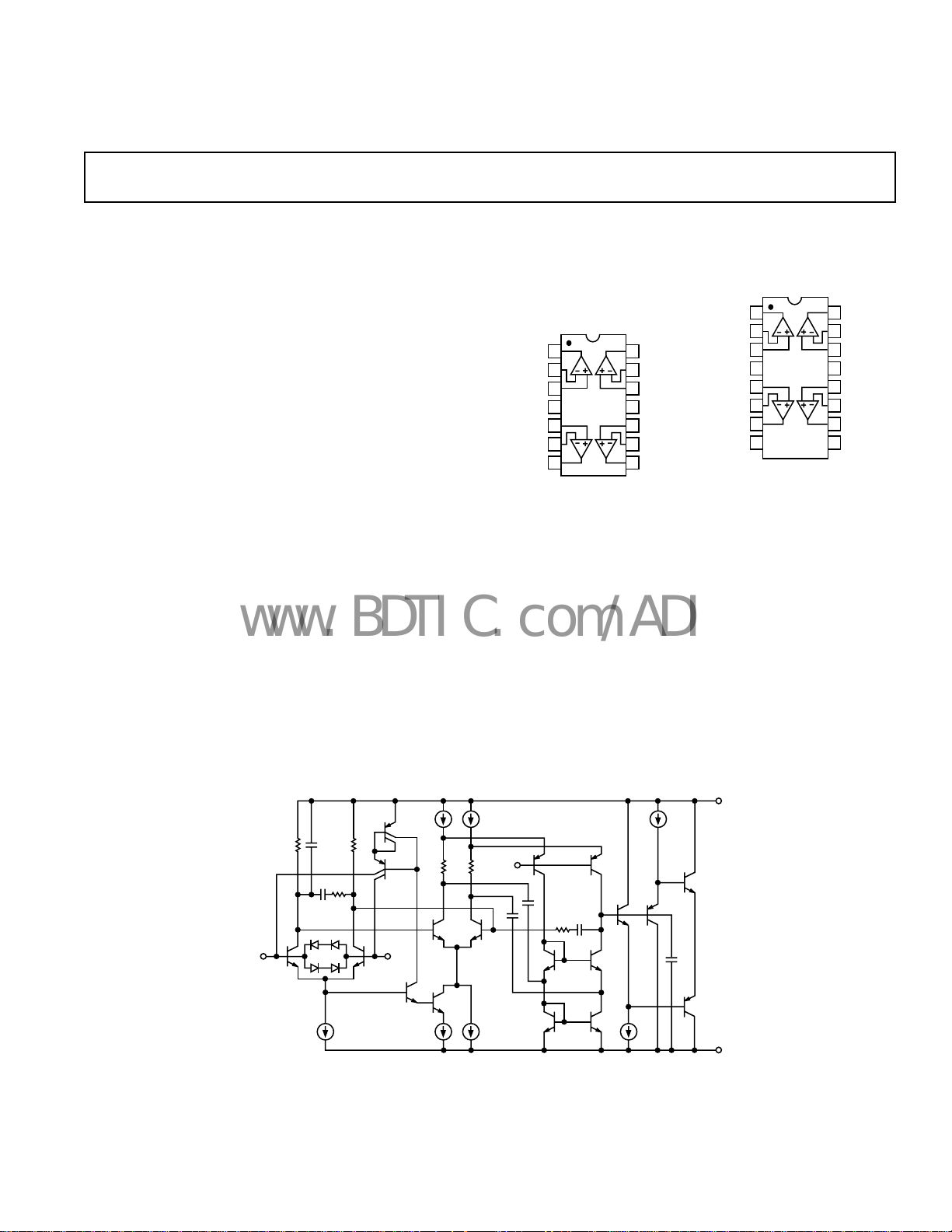
PIN CONNECTIONS
14-Lead Hermetic DIP
(Y-Suffix)
14-Lead Plastic DIP
(P-Suffix)
OUT A
–IN A
+IN A
+IN B
–IN B
OUT B
1
2
3
4
V+
OP470
5
6
7
14
13
12
11
10
9
8
OUT D
–IN D
+IN D
V–
+IN C
–IN C
OUT C
The OP470 offers excellent amplifier matching which is important for applications such as multiple gain blocks, low noise
instrumentation amplifiers, quad buffers, and low noise active
filters.
The OP470 conforms to the industry standard 14-lead DIP
pinout. It is pin compatible with the LM148/149, HA4741,
HA5104, and RM4156 quad op amps and can be used to upgrade systems using these devices.
For higher speed applications, the OP471, with a slew rate of 8
V/ms, is recommended.
16-Lead SOIC Package
(S-Suffix)
1
OUT A OUT D
2
–IN A –IN D
3
+IN A +IN D
4
V+ V–
OP470
5
+IN B +IN C
6
–IN B –IN C
7
OUT B OUT C
8
NC NC
NC = NO CONNECT
16
15
14
13
12
11
10
9
SIMPLIFIED SCHEMATIC
IN
+IN
REV. B
Information furnished by Analog Devices is believed to be accurate and
reliable. However, no responsibility is assumed by Analog Devices for its
use, nor for any infringements of patents or other rights of third parties that
may result from its use. No license is granted by implication or otherwise
under any patent or patent rights of Analog Devices.
V+
BIAS
V–
One Technology Way, P.O. Box 9106, Norwood, MA 02062-9106, U.S.A.
Tel: 781/329-4700 www.analog.com
Fax: 781/326-8703 © Analog Devices, Inc., 2002
Page 2
OP470–SPECIFICATIONS
www.BDTIC.com/ADI
ELECTRICAL CHARACTERISTICS
(at VS = 15 V, TA = 25C, unless otherwise noted.)
OP470A/E OP470F OP470G
Parameter Symbol Conditions Min Typ Max Min Typ Max Min Typ Max Unit
INPUT OFFSET
VOLTAGE V
OS
0.1 0.4 0.2 0.8 0.4 1.0 mV
INPUT OFFSET
CURRENT I
OS
VCM = 0 V 3 10 6 20 12 30 nA
INPUT BIAS
CURRENT I
B
VCM = 0 V 6 25 15 50 25 60 nA
INPUT NOISE
VOLTAGE e
np-p
0.1 Hz to 10 Hz 80 200 80 200 80 200 nV p-p
(Note 1)
INPUT NOISE f
Voltage Density e
n
= 10 Hz 3.8 6.5 3.8 6.5 3.8 6.5
O
fO = 100 Hz 3.3 5.5 3.3 5.5 3.3 5.5 nV÷Hz
f
1 kHz 3.2 5.0 3.2 5.0 3.2 5.0
O =
(Note 2)
INPUT NOISE f
Current Density i
n
= 10 Hz 1.7 1.7 1.7
O
fO = 100 Hz 0.7 0.7 0 7 pA÷Hz
fO = 1 kHz 0.4 0.4 0.4
LARGE-SIGNAL V = ± 10 V
Voltage Gain A
VO
RL = 10 kW 1000 2300 800 1700 800 1700 V/mV
RL = 2 kW 500 1200 400 900 400 900
INPUT VOLTAGE
RANGE IVR (Note 3) ± 11 ± 12 ± 11 ±12 ± 11 ± 12 V
OUTPUT VOLTAGE
SWING V
O
RL ≥ 2 kW±12 ± 13 ± 12 ± 13 ± 12 ± 13 V
COMMON-MODE
REJECTION CMR V
= ± 11 V 110 125 100 120 100 120 dB
CM
POWER SUPPLY
REJECTION RATIO PSRR VS = ± 4.5 V to ± 18 V 0.56 1.8 1.0 5.6 1.0 5.6 mV/V
SLEW RATE SR 1.4 2 1.4 2 1.4 2 V/ms
SUPPLY CURRENT
(All Amplifiers) I
SY
No Load 9 11911911mA
GAIN BANDWIDTH
PRODUCT GBW AV = 10 666MHz
CHANNEL
SEPARATION CS VO = 20 V p-p 125 155 125 155 125 155 dB
fO = 10 Hz (Note 1)
INPUT
CAPACITANCE C
INPUT RESISTANCE R
IN
IN
222pF
0.4 0.4 0.4 MW
Differential-Mode
INPUT RESISTANCE
Common-Mode R
SETTLING TIME t
INCM
S
= 1
A
V
to 0.1% 5.5 5.5 5.5 ms
11 11 11 GW
to 0.01 % 6.0 6.0 6.0
NOTES
1
Guaranteed but not 100% tested
2
Sample tested
3
Guaranteed by CMR test
–2–
REV. B
Page 3
OP470
www.BDTIC.com/ADI
ELECTRICAL CHARACTERISTICS
(at VS = 15 V, –55C £ TA £ 125C for OP470A, unless otherwise noted.)
OP470A
Parameter Symbol Conditions Min Typ Max Unit
INPUT OFFSET VOLTAGE V
OS
0.14 0.6 mV
AVERAGE INPUT
Offset Voltage Drift TCV
INPUT OFFSET CURRENT I
INPUT BIAS CURRENT I
OS
OS
B
LARGE-SIGNAL V
Voltage Gain A
VO
VCM = 0 V 5 20 nA
VCM = 0 V 15 20 nA
= ± 10 V
O
RL = 10 kW 750 1600 V/mV
0.4 2 mV/∞C
RL = 2 kW 400 800
INPUT VOLTAGE RANGE*IVR ± 11 ± 12 V
OUTPUT VOLTAGE SWING V
O
RL ≥ 2 kW±12 ± 13 V
COMMON-MODE
REJECTION CMR V
= ± 11 V 100 120 dB
CM
POWER SUPPLY
REJECTION RATIO PSRR VS = ± 4.5 V to ± 18 V 1.0 5.6 mV/V
SUPPLY CURRENT
(All Amplifiers) I
*
Guaranteed by CMR test
SY
No Load — 9.2 11 mA
(at VS = 15 V, –25C £ TA £ 85C for OP470E/OP470EF, –40C £ TA £ 85C for OP470G,
ELECTRICAL CHARACTERISTICS
unless otherwise noted.)
OP470E OP470F OP470G
Parameter Symbol Conditions Min Typ Max Min Typ Max Min Typ Max Unit
INPUT OFFSET
VOLTAGE V
OS
0.12 0.5 0.24 1.0 0.5 1.5 mV
AVERAGE INPUT
Offset Voltage Drift TCV
OS
0.4 2 0.6 4 2 mV/∞C
INPUT OFFSET
CURRENT I
OS
VCM = 0 V 4 20 7 40 20 50 nA
INPUT BIAS
CURRENT I
B
LARGE-SIGNAL V
Voltage Gain A
VO
VCM = 0 V 11 50 2070 4075 nA
= ± 10 V
O
RL = 10 kW 800 1800 600 1400 600 1500 V/mV
RL = 2 kW 400 900 300 700 300 800
INPUT VOLTAGE
RANGE
*
IVR ± 11 ± 12 ± 11 ± 12 ± 11 ± 12 V
OUTPUT VOLTAGE
SWING V
O
RL ≥ 2 kW±12 ± 13 ± 12 ± 13 ± 12 ± 13 V
COMMON-MODE
REJECTION CMR V
= ± 11 V 100 120 90 115 90 110 dB
CM
POWER SUPPLY
REJECTION RATIO PSRR VS = ± 4.5 V to ± 18 V 0.7 5.6 1.8 10 1.8 10 mV/V
SUPPLY CURRENT
(All Amplifiers) I
*
Guaranteed by CMR test
SY
No Load — 9.2 11 — 9.2 11 — 9.3 11 mA
REV. B
–3–
Page 4
OP470–SPECIFICATIONS
www.BDTIC.com/ADI
WAFER TEST LIMITS
Parameter Symbol Conditions Limit Unit
INPUT OFFSET VOLTAGE V
INPUT OFFSET CURRENT I
INPUT BIAS CURRENT I
LARGE-SIGNAL V
Voltage Gain A
INPUT VOLTAGE RANGE*IVR ± 11 V Min
OUTPUT VOLTAGE SWING V
COMMON-MODE
REJECTION CMR V
POWER SUPPLY
REJECTION RATIO PSRR VS = ± 4.5 V to ± 18 V 5.6 mV/V Max
SUPPLY CURRENT
(All Amplifiers) I
NOTE
*
Guaranteed by CMR test
Electrical tests are performed at wafer probe to the limits shown. Due to variations in assembly methods and normal yield loss, yield after packaging is not guaranteed for standard product dice. Consult factory to negotiate specifications based on dice lot qualification through sample lot assembly and testing.
(at VS = 15 V, 25C, unless otherwise noted.)
OS
OS
B
VO
O
SY
VCM = 0 V 20 nA Max
VCM = 0 V 50 nA Min
= ± 10 V
O
RL = 10 kW 800 V/mV Min
RL = 2 kW 400
RL ≥ 2 kW±12 V Min
= ± 11 V 100 dB
CM
No Load 11 mA Max
OP470GBC
0.8 mV Max
–4–
REV. B
Page 5
OP470
WARNING!
ESD SENSITIVE DEVICE
www.BDTIC.com/ADI
ABSOLUTE MAXIMUM RATINGS
Supply Voltage . . . . . . . . . . . . . . . . . . . . . . . . . . . . . . . . ± 18 V
Differential Input Voltage
Differential Input Current
2
. . . . . . . . . . . . . . . . . . . . . . ± 1.0 V
2
. . . . . . . . . . . . . . . . . . . . ± 25 mA
1
Input Voltage . . . . . . . . . . . . . . . . . . . . . . . . . . Supply Voltage
Output Short-Circuit Duration . . . . . . . . . . . . . . . Continuous
Storage Temperature Range
P, Y Package . . . . . . . . . . . . . . . . . . . . . . –65∞C to +150∞C
Lead Temperature Range (Soldering 60 sec) . . . . . . . . . 300∞C
Junction Temperature (T
) . . . . . . . . . . . . . –65∞C to +150∞C
j
Operating Temperature Range
OP470A . . . . . . . . . . . . . . . . . . . . . . . . . –55∞C to +125∞C
OP470E, OP470F . . . . . . . . . . . . . . . . . . . –25∞C to +85∞C
OP470G . . . . . . . . . . . . . . . . . . . . . . . . . . –40∞C to +85∞C
ORDERING GUIDE
Package Options
T
= 25∞C Operating
A
V
max Cerdip Temperature
OS
(V) 14-Pin Plastic Range
400 MIL
400 OP470AY* MIL
400 OP470EY IND
800 OP470FY* IND
1000 OP470GP XIND
1000 OP470GS XIND
*Not for new design; obsolete April 2002.
For military processed devices, please refer to the standard
Microcircuit Drawing (SMD) available at
www.dscc.dla.mil/programs/milspec/default.asp
SMD Part Number ADI Equivalent
59628856501CA OP470AYMDA
596288565012A OP470ARCMDA
596288565013A
*
Not for new designs; obsolete April 2002.
*
OP470ATCMDA
Package Type
3
JA
JC
Unit
14-Lead Hermetic DIP(Y) 94 10 ∞C/W
14-Lead Plastic DIP(P) 76 33 ∞C/W
16-Lead SOIC (S) 88 23 ∞C/W
NOTES
1
Absolute Maximum Ratings apply to both DICE and packaged parts, unless
otherwise noted.
2
The OP470’s inputs are protected by back-to-back diodes. Current limiting
resistors are not used in order to achieve low noise performance. If differential
voltage exceeds ± 1.0 V, the input current should be limited to ± 25 mA.
3
is specified for worst case mounting conditions, i.e., JA is specified for device
JA
in socket for TO, CerDIP, PDIP, packages; JA is specified for device soldered to
printed circuit board for SOIC packages.
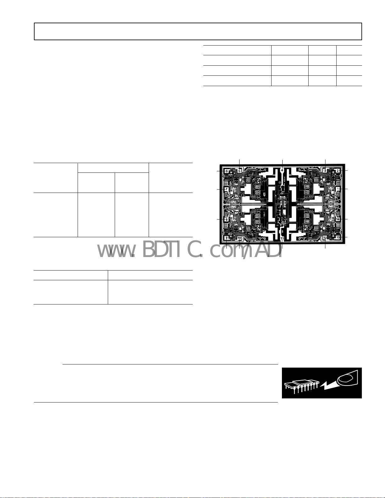
–IN B
OUT B
OUT C
+IN B
–IN C
+IN C V– +IN D
DIE SIZE 0.163 0.106 INCH, 17,278 SQ. mm
(4.14 2.69 mm, 11.14 SQ. mm)
+IN AV+
–IN A
OUT A
OUT D
–IN D
Figure 1. Dice Characteristics
CAUTION
ESD (electrostatic discharge) sensitive device. Electrostatic charges as high as 4000 V readily
accumulate on the human body and test equipment and can discharge without detection. Although
the OP470 features proprietary ESD protection circuitry, permanent damage may occur on devices
subjected to high energy electrostatic discharges. Therefore, proper ESD precautions are
recommended to avoid performance degradation or loss of functionality.
REV. B
–5–
Page 6

OP470
www.BDTIC.com/ADI
10
9
8
7
6
5
4
3
–Typical Performance Characteristics
5
T
TA = 25C
= 15V
V
S
= 25C
A
4
3
AT 10Hz
AT 1kHz
5mV
100
90
1s
I/F CORNER = 5Hz
2
VOLTA G E NOISE – nV/ Hz
1
1
10 100 1k
FREQUENCY – Hz
TPC 1. Voltage Noise Density vs.
Frequency
10.0
TA = 25C
= 15V
V
S
1.0
CURRENT NOISE – pA/ Hz
I/F CORNER = 200Hz
0.1
10 10k
100 1k
FREQUENCY – Hz
TPC 4. Current Noise Density vs.
Frequency
2
VOLTA G E NOISE – nV/ Hz
1
0 5 20
10 15
SUPPLY VOLTAGE – V
TPC 2. Voltage Noise Density vs.
Supply Voltage
140
VS = 15V
120
100
80
60
40
INPUT OFFSET VOLTAGE – V
20
0
–75
–50 –25 0 25 50 75 100 125
TEMPERATURE – C
TPC 5. Input Offset Voltage vs.
Temperature
10
0%
NOISE VOLTAGE – 100nV/DIV
0246810
TIME – Secs
TA = 25C
= 15V
V
S
TPC 3. 0.1 Hz to 10 Hz Noise
10
TA = 25C
9
= 15V
V
S
8
7
6
5
4
3
2
CHANGE IN OFFSET VOLTAGE – V
1
0
1 2345
0
TIME – Mins
TPC 6. Warm-Up Offset Voltage Drift
20
15
10
5
INPUT BIAS CURRENT – nA
0
–75
–50 –25 0 25 50 75 100 125
TEMPERATURE – C
VS = 15V
V
CM
TPC 7. Input Bias Current vs.
Temperature
= 0V
10
VS = 15V
9
= 0V
V
CM
8
7
6
5
4
3
2
INPUT OFFSET CURRENT – nA
1
0
–50 –25 0 25 50 75 100 125
–75
TEMPERSTURE – C
TPC 8. Input Offset Current vs.
Temperature
–6–
9
TA = 25C
= 15V
V
S
8
7
6
5
INPUT BIAS CURRENT – nA
4
–7.5 –2.5 2.5 7.5 12.5
–12.5
COMMON-MODE VOLTAGE – V
TPC 9. Input Bias Current vs.
Common-Mode Voltage
REV. B
Page 7

OP470
www.BDTIC.com/ADI
130
120
110
100
90
80
70
60
CMR – dB
50
40
30
20
10
10 100 1k 10k 100k 1M
1
FREQUENCY – Hz
TPC 10. CMR vs. Frequency
140
130
120
110
100
90
80
70
60
PSR – dB
50
40
30
20
10
0
1
+PSR
10 100 1k 10k 100k 1M 10M 100M
FREQUENCY – Hz
TPC 13. PSR vs. Frequency
TA = 25C
= 15V
V
S
TA = 25C
–PSR
10
TA = +25C
8
6
4
TOTA L SUPPLY CURRENT – mA
2
0 5 20
TA = +125C
TA = –55C
10 15
SUPPLY VOLTAGE – V
TPC 11. Total Supply Current vs.
Supply Voltage
140
130
120
110
100
90
80
70
60
50
40
OPEN-LOOP GAIN – dB
30
20
10
0
10 100 1k 10k 100k 1M 10M 100M
1
FREQUENCY – Hz
TA = 25C
= 15V
V
S
TPC 14. Open-Loop Gain vs. Frequency
10
VS = 15V
9
8
7
6
5
4
TOTA L SUPPLY CURRENT – mA
3
2
–50 –25 0 25 50 75 100 125
–75
TEMPERSTURE – C
TPC 12. Total Supply Current vs.
Supply Voltage
80
60
40
20
CLOSED-LOOP GAIN – dB
0
–20
1k
10k 100k 1M 10M
FREQUENCY – Hz
TPC 15. Closed-Loop Gain vs.
Frequency
25
20
15
10
5
GAIN – dB
0
–5
–10
1
PHASE
GAIN
2345
FREQUENCY – MHz
TA = 25C
= 15V
V
S
PHASE MARGIN
= 58
67 89
TPC 16. Open-Loop Gain, Phase
Shift vs. Frequency
80
100
120
140
160
180
PHASE SHIFT – Degrees
200
220
10
TPC 17. Open-Loop Gain vs. Supply
Voltage
5000
4000
3000
2000
OPEN-LOOP GAIN – V/mV
1000
TA = 25C
= 10k
R
L
0
0
5 10 15 20 25
SUPPLY VOLTAGE – V
REV. B
–7–
80
GBW
70
60
50
PHASE MARGIN – Degrees
40
–50 –25 0 25 50 75 100 125 150
–75
TEMPERATURE – C
VS = 15V
TPC 18. Gain-Bandwidth Product,
Phase Margin vs. Temperature
8
6
4
2
GAIN-BANDWIDTH PRODUCT – MHz
0
Page 8

OP470
www.BDTIC.com/ADI
28
24
20
16
12
8
PEAK-TO-PEAK AMPLITUDE – V
4
0
1k
10k 100k 1M 10M
FREQUENCY – Hz
TA = 25C
= 15V
V
S
THD = 1%
TPC 19. Maximum Output Swing vs.
Frequency
360
TA = 25C
= 15V
V
S
300
240
180
120
OUTPUT IMPEDANCE –
60
0
100
AV = 100
AV = 1
1k 10k 100k 1M 10M 100M
FREQUENCY – Hz
TPC 22. Output Impedance vs.
Frequency
20
TA = 25C
18
= 15V
V
S
16
14
12
10
8
6
MAXIMUM OUTPUT – V
4
2
0
100
POSITIVE
SWING
NEGATIVE
SWING
LOAD RESISTANCE –
1k 10k
TPC 20. Maximum Output Voltage
vs. Load Resistance
4.0
VS = 15V
3.5
3.0
2.5
2.0
SLEW RATE – V/s
1.5
1.0
–50 –25 0 25 50 75 100 125
–75
TEMPERATURE – C
–SR
+SR
TPC 23. Slew Rate vs. Temperature
100
TA = 25C
= 15V
V
S
= 100mV
V
80
IN
= 1
A
V
60
40
OVERSHOOT – %
20
0
0
200 400 600 800 1000
CAPACITIVE LOAD – pF
TPC 21. Small-Signal Overshoot vs.
Capacitive Load
170
160
150
140
130
120
110
100
90
80
CHANNEL SEPARATION – dB
70
60
50
10
100 1k 10k 100k 1M 10M
TA = 25C
= 15V
V
S
= 20V p-p TO 10kHz
V
O
FREQUENCY – Hz
TPC 24. Channel Separation vs.
Frequency
1
TA = 25C
= 15V
V
S
= 10V p-p
V
O
= 2k
R
L
0.1
0.01
DISTORTION – %
0.001
10
AV = –10
AV = 1
100 1k 10k
FREQUENCY – Hz
TPC 25. Total Harmonic Distortion
vs. Frequency
100
90
10
0%
5V
TPC 26. Large-Signal Transient
Response
–8–
TA = 25C
= 15V
V
S
= 1
A
V
20µs
TA = 25C
= 15V
V
100
90
10
0%
50mV
S
A
V
0.2µs
= 1
TPC 27. Small-Signal Transient
Response
REV. B
Page 9

OP470
www.BDTIC.com/ADI
5k
500
1/4
OP470
50k
50
1/4
OP470
CHANNEL SEPARATION = 20 LOG
V
20V p-p
1
V
2
V
1
V2/1000
Figure 2. Channel Separation Test Circuit
+18V
+1V
–1V
2
4
1
A
3
11
–18V
9
C
10
+1V
8
–1V
6
5
13
12
7
B
14
D
Figure 3. Burn-In Circuit
APPLICATIONS INFORMATION
Voltage and Current Noise
The OP470 is a very low-noise quad op amp, exhibiting a typical voltage noise of only 3.2 nV÷Hz @ 1 kHz. The exceptionally
low-noise characteristics of the OP470 are in part achieved by
operating the input transistors at high collector currents since
the voltage noise is inversely proportional to the square root of
the collector current. Current noise, however, is directly proportional to the square root of the collector current. As a result, the
outstanding voltage noise performance of the OP470 is gained
at the expense of current noise performance, which is typical for
low noise amplifiers.
To obtain the best noise performance in a circuit, it is vital to
understand the relationship between voltage noise (e
noise (i
), and resistor noise (et).
n
), current
n
TOTAL NOISE AND SOURCE RESISTANCE
The total noise of an op amp can be calculated by:
EeiR e
nnnS t
222
=
()+()+()
where:
= total input referred noise
E
n
e
= up amp voltage noise
n
i
= op amp current noise
n
e
= source resistance thermal noise
t
R
= source resistance
S
The total noise is referred to the input and at the output would
be amplified by the circuit gain. Figure 4 shows the relationship
between total noise at 1 kHz and source resistance. For R
< 1 kW
S
the total noise is dominated by the voltage noise of the OP470.
As R
rises above 1 kW, total noise increases and is dominated
S
by resistor noise rather than by voltage or current noise of the
OP470. When R
exceeds 20 kW, current noise of the OP470
S
becomes the major contributor to total noise.
Figure 5 also shows the relationship between total noise and
source resistance, but at 10 Hz. Total noise increases more
quickly than shown in Figure 4 because current noise is inversely
proportional to the square root of frequency. In Figure 5, current
noise of the OP470 dominates the total noise when R
> 5 kW.
S
From Figures 4 and 5 it can be seen that to reduce total noise,
source resistance must be kept to a minimum. In applications
with a high source resistance, the OP400, with lower current
noise than the OP470, will provide lower total noise.
100
OP11
OP400
10
OP471
TOTAL NOISE – nV/ Hz
OP470
RESISTOR
NOISE ONLY
1
100 100k
RS – SOURCE RESISTANCE –
10k1k
Figure 4. Total Noise vs. Source Resistance (Including
Resistor Noise) at 1 kHz
100
OP11
OP400
10
OP471
TOTAL NOISE – nV/ Hz
OP470
RESISTOR
NOISE ONLY
1
100 100k
RS – SOURCE RESISTANCE –
10k1k
Figure 5. Total Noise vs. Source Resistance (Including
Resistor Noise) at 10 Hz
REV. B
–9–
Page 10

OP470
www.BDTIC.com/ADI
Figure 6 shows peak-to-peak noise versus source resistance over
the 0.1 Hz to 10 Hz range. Once again, at low values of R
, the
S
voltage noise of the OP470 is the major contributor to peak-to-peak
noise with current noise the major contributor as R
increases.
S
The crossover point between the OP470 and the OP400 for
peak-to-peak noise is at R
= 17 kW.
S
The OP471 is a higher speed version of the OP470, with a slew
rate of 8 V/ms. Noise of the OP471 is only slightly higher than
the OP470. Like the OP470, the OP471 is unity-gain stable.
1000
OP11
OP400
OP471
100
OP470
RESISTOR
PEAK-TO-PEAK NOISE – nV/ Hz
10
100 100k
NOISE ONLY
RS – SOURCE RESISTANCE –
10k1k
Figure 6. Peak-To-Peak Noise (0.1 Hz to 10 Hz) vs. Source
Resistance (Includes Resistor Noise)
For reference, typical source resistances of some signal sources
are listed in Table I.
R3
1.24k
R1
5
R2
5
OP470
DUT
200
OP27E
909
R4
C1
2F
R5
R6
600k
D1
1N4148D21N4148
R8
10k
OP15E
Table I.
Device
Source Impedance Comments
Strain gage <500 W Typically used in
low frequency applications.
Magnetic <1500 W Low I
very important to reduce
B
tapehead self-magnetization problems
when direct coupling is used.
OP470 IB can be neglected.
Magnetic <1500 W Similar need for low I
in direct
B
phonograph coupled applications. OP470
cartridges will not introduce any self-
magnetization problem.
Linear variable <1500 W Used in rugged servo-feedback
differential applications. Bandwidth of
transformer interest is 400 Hz to 5 kHz.
For further information regarding noise calculations, see “Minimization of Noise
in Op Amp Applications,” Application Note AN-15.
NOISE MEASUREMENTS— PEAK-TO-PEAK VOLTAGE NOISE
The circuit of Figure 7 is a test setup for measuring peak-to-peak
voltage noise. To measure the 200 nV peak-to-peak noise specification of the OP470 in the 0.1 Hz to 10 Hz range, the following
precautions must be observed:
1. The device must be warmed up for at least five minutes. As
shown in the warm-up drift curve, the offset voltage typically changes 5 mV due to increasing chip temperature after
power-up. In the 10-second measurement interval, these
temperature-induced effects can exceed tens of nanovolts.
2. For similar reasons, the device must be well-shielded from
air currents. Shielding also minimizes thermocouple effects.
3. Sudden motion in the vicinity of the device can also “feedthrough”
to increase the observed noise.
C4
0.22F
R9
306k
C2
0.032F
R10
65.4k
R11
65.4k
C3
0.22F
R12
10k
OP15E
R13
5.9k
GAIN = 50,000
V
S
= 5V
R14
4.99k
C5
1F
e
OUT
Figure 7. Peak-To-Peak Voltage Noise Test Circuit (0.1 Hz to 10 Hz)
–10–
REV. B
Page 11

OP470
www.BDTIC.com/ADI
4. The test time to measure 0.1 Hz to 10 Hz noise should not exceed 10 seconds. As shown in the noise-tester frequency-response
curve of Figure 8, the 0.1 Hz corner is defined by only one pole.
The test time of 10 seconds acts as an additional pole to eliminate noise contribution from the frequency band below 0.1 Hz.
5. A noise-voltage-density test is recommended when measuring
noise on a large number of units. A 10 Hz noise voltage-density
measurement will correlate well with a 0.1 Hz to 10 Hz
peak-to-peak noise reading, since both results are determined
by the white noise and the location of the 1/f corner frequency.
6. Power should be supplied to the test circuit by well bypassed
low noise supplies, e.g. batteries. These will minimize output
noise introduced via the amplifier supply pins.
100
80
60
GAIN – dB
40
20
0
0.01
0.1 1 10 100
FREQUENCY – Hz
Figure 8. 0.1 Hz to 10 Hz Peak-to-Peak Voltage Noise Test
Circuit Frequency Response
NOISE MEASUREMENT—NOISE VOLTAGE DENSITY
The circuit of Figure 9 shows a quick and reliable method of
measuring the noise voltage density of quad op amps. Each
individual amplifier is series-connected and is in unity-gain, save
the final amplifier which is in a noninverting gain of 101. Since
the ac noise voltages of each amplifier are uncorrelated, they
add in rms fashion to yield:
Ê
e=101 e + e e e
OUT nA nB nC nD
22 2 2
Ë
++
ˆ
¯
The OP470 is a monolithic device with four identical amplifiers.
The noise voltage density of each individual amplifier will match,
giving:
e 101 4e = 101 2e
OUT n n
Ê
=
Ë
ˆ
2
¯
()
NOISE MEASUREMENT—CURRENT NOISE DENSITY
The test circuit shown in Figure 10 can be used to measure
current noise density. The formula relating the voltage output to
current noise density is:
2
ˆ
Ê
nOUT
-
40nV / Hz
˜
Á
G
Ë
i
=
n
()
¯
R
S
2
where:
G = gain of 10000
R
= 100 kW source resistance
S
R3
1.24k
R1
5
R2
100k
OP470
DUT
200
OP27E
R5
8.06k
R4
en OUT TO
SPECTRUM ANALYZER
GAIN = 50,000
V
= 5V
S
Figure 10. Current Noise Density Test Circuit
1/4
1/4
OP470
OP470
Figure 9. Noise Voltage Density Test Circuit
REV. B
1/4
OP470
–11–
R1
100
10k
1/4
OP470
e
(nV Hz) = 101(2en)
OUT
= 15V
V
S
R2
TO SPECTRUM ANALYZER
e
OUT
Page 12

OP470
www.BDTIC.com/ADI
CAPACITIVE LOAD DRIVING AND POWER SUPPLY CONSIDERATIONS
The OP470 is unity-gain stable and is capable of driving large
capacitive loads without oscillating. Nonetheless, good supply
bypassing is highly recommended. Proper supply bypassing
reduces problems caused by supply line noise and improves the
capacitive load driving capability of the OP470.
In the standard feedback amplifier, the op amp’s output resistance
combines with the load capacitance to form a low pass filter that
adds phase shift in the feedback network and reduces stability.
A simple circuit to eliminate this effect is shown in Figure 11.
The added components, C1 and R3, decouple the amplifier
from the load capacitance and provide additional stability. The
values of C1 and R3 shown in Figure 11 are for a load capacitance of up to 1000 pF when used with the OP470.
V
IN
R1
100*
*SEE TEXT
V+
OP470
*
V–
C2
10F
+
C3
0.1F
R2
C1
1000pF
0.1F
R3
50
C4
10F
+
C5
PLACE SUPPLY DECOUPLING
CAPACITORS AT OP470
V
OUT
C
L
1000pF
Figure 11. Driving Large Capacitive Loads
In applications where the OP470’s inverting or noninverting
inputs are driven by a low source impedance (under 100 W) or
connected to ground, if V+ is applied before V–, or when V is
disconnected, excessive parasitic currents will flow. Most applications use dual tracking supplies and with the device supply pins
properly bypassed, power-up will not present a problem. A source
resistance of at least 100 W in series with all inputs (Figure 11)
will limit the parasitic currents to a safe level if V– is disconnected. It should be noted that any source resistance, even 100 W,
adds noise to the circuit. Where noise is required to be kept at a
minimum, a germanium or Schottky diode can be used to clamp
the V- pin and eliminate the parasitic current flow instead of
using series limiting resistors. For most applications, only one
diode clamp is required per board or system.
R1
OP470
2V/s
Figure 12. Pulsed Operation
During the fast feedthrough-like portion of the output, the input
protection diodes effectively short the output to the input, and a
current, limited only by the output short-circuit protection, will
be drawn by the signal generator. With Rf £ 500 W, the output
is capable of handling the current requirements (IL < 20 mA at
10 V); the amplifier will stay in its active mode and a smooth
transition will occur.
When Rf > 3 kW, a pole created by Rf and the amplifier’s input
capacitance (2 pF) creates additional phase shift and reduces
phase margin. A small capacitor (20 pF to 50 pF) in parallel
with Rf helps eliminate this problem.
APPLICATIONS
Low Noise Amplifier
A simple method of reducing amplifier noise by paralleling
amplifiers is shown in Figure 13. Amplifier noise, depicted in
Figure 14, is around 2 nV/÷Hz @ 1 kHz (R.T.I.). Gain for each
paralleled amplifier and the entire circuit is 1000. The 200 W
resistors limit circulating currents and provide an effective output resistance of 50 W. The amplifier is stable with a 10 nF
capacitive load and can supply up to 30 mA of output drive.
+15V
V
IN
R1
50
R4
50
R7
50
1/4
OP470E
–15V
1/4
OP470E
1/4
OP470E
R2
50k
R5
50k
R8
50k
R3
200
R6
200
R9
200
V
OUT
= 1000V
IN
UNITY-GAIN BUFFER APPLICATIONS
When Rf £ 100 W and the input is driven with a fast, large
signal pulse(> 1 V), the output waveform will look as shown
in Figure 12.
–12–
R12
R11
50k
200
R10
50
1/4
OP470E
Figure 13. Low Noise Amplifier
REV. B
Page 13

100
10
0%
100
90
1ms
5V5V
A OUT
A OUT
www.BDTIC.com/ADI
90
REFERRED TO INPUT
10
0%
NOISE DENSITY – 0.58nV/ Hz/DIV
OP470
Figure 14. Noise Density of Low Noise Amplifier, G = 1000
DIGITAL PANNING CONTROL
Figure 15 uses a DAC-8408, quad 8-bit DAC to pan a signal
between two channels. The complementary DAC current outputs two of the DAC-8408’s four DACs drive current-to-voltage
converters built from a single quad OP470. The amplifiers have
complementary outputs with the amplitudes dependent upon
the digital code applied to the DAC. Figure 16 shows the complementary outputs for a 1 kHz input signal and digital ramp applied
to the DAC data inputs. Distortion of the digital panning control is less than 0.01%.
5V
SIDE A IN
DAC- 8408GP
V
A
REF
V
DD
DAC A
DAC B
I
I
OUT2A/2B
Figure 16. Digital Panning Control Output
Gain error due to the mismatching between the internal DAC
ladder resistors and the current-to-voltage feedback resistors is
eliminated by using feedback resistors internal to the DAC. Of
the four DACs available in the DAC-8408, only two DACs, A
and C, actually pass a signal. DACs B and D are used to provide the additional feedback resistors needed in the circuit. If
the VREFB and VREFD inputs remain unconnected, the
current-to-voltage converters using RFBB and RFBD are unaffected by digital data reaching DACs B and D.
RFBA
+15V
OUT1A
I
OUT1B
20pF
20pF
1/4
OP470E
–15V
1/4
OP470E
A OUT
A OUT
V
C
SIDE B IN
DAC DATA BUS
PINS 9 (LSB) – 16 (MSB)
5V
DAC SELECT
1k
1k
REF
A/B
R/W
DS1
DS2
DAC C
DAC D
DGND
Figure 15. Digital Panning Control Circuit
REV. B
RFBB
RFBC
I
OUT1C
I
OUT2C/2D
I
OUT1D
RFBD
–13–
20pF
20pF
1/4
OP470E
1/4
OP470E
B OUT
B OUT
Page 14

OP470
www.BDTIC.com/ADI
SQUELCH AMPLIFIER
The circuit of Figure 17 is a simple squelch amplifier that uses a
FET switch to cut off the output when the input signal falls
below a preset limit.
The input signal is sampled by a peak detector with a time
constant set by C1 and R6. When the output of the peak detector
(Vp), falls below the threshold voltage, (VTH), set by R8, the
comparator formed by op amp C switches from V– to V+. This
drives the gate of the N-channel FET high, turning it ON, reducing the gain of the inverting amplifier formed by op amp A
to zero.
– –5V
OUT
C1
1FR61M
V+
D2
1N4148
IN
R6
10k
R7
10k
1/4
OP470E
C
R4
10M
C2
10F
+
R5
100k
2N5434
R2
R1
2k
V
IN
R3
2k
10k
1/4
OP470E
A
R4
10k
1/4
OP470E
B
= 1 SECOND
V
D1
1N4148
Figure 17. Squelch Amplifier
FIVE-BAND LOW-NOISE STEREO GRAPHIC EQUALIZER
The graphic equalizer circuit shown in Figure 18 provides 15 dB
of boost or cut over a 5-band range. Signal-to-noise ratio over a
20 kHz bandwidth is better than 100 dB referred to a 3 V rms
input. Larger inductors can be replaced by active inductors but
this reduces the signal-to-noise ratio.
C1
0.47F
V
IN
47k
1/4
R1
OP470E
C2
R3
6.8F
680
+
TANTALUM
C3
R5
1F
680
+
TANTALUM
C4
R7
0.22F
680
+
TANTALUM
C5
R9
0.047F
680
+
TANTALUM
C6
R11
0.022F
680
+
TANTALUM
1H
1H
1H
1H
1H
L1
L2
L3
L4
L5
R2
3.3k
R4
1k
R4
1k
R4
1k
R4
1k
R4
1k
60Hz
200Hz
800Hz
3kHz
10kHz
1/4
OP470E
R13
3.3k
R14
100
V
OUT
Figure 18. Five-Band Low Noise Graphic Equalizer
–14–
REV. B
Page 15

OUTLINE DIMENSIONS
www.BDTIC.com/ADI
14-Lead Ceramic Dip-Glass Hermetic Seal [CERDIP]
(Q-14)
Dimensions shown in inches and (millimeters)
0.005 (0.13) MIN
PIN 1
0.200 (5.08)
0.200 (5.08)
0.125 (3.18)
CONTROLLING DIMENSIONS ARE IN INCHES; MILLIMETERS DIMENSIONS
(IN PARENTHESES) ARE ROUNDED-OFF INCH EQUIVALENTS FOR
REFERENCE ONLY AND ARE NOT APPROPRIATE FOR USE IN DESIGN
0.785 (19.94) MAX
MAX
0.023 (0.58)
0.014 (0.36)
0.098 (2.49) MAX
14
17
0.100 (2.54) BSC
8
0.070 (1.78)
0.030 (0.76)
0.310 (7.87)
0.220 (5.59)
0.060 (1.52)
0.015 (0.38)
SEATING
PLANE
0.150
(3.81)
MIN
0.320 (8.13)
0.290 (7.37)
15
0
0.015 (0.38)
0.008 (0.20)
16-Lead Standard Small Outline Package [SOIC]
Wide Body
(RW-16)
Dimensions shown in millimeters and (inches)
10.50 (0.4134)
10.10 (0.3976)
OP470
14-Lead Plastic Dual-in-Line Package [PDIP]
(N-14)
Dimensions shown in inches and (millimeters)
0.685 (17.40)
0.665 (16.89)
0.645 (16.38)
14
1
0.100 (2.54)
BSC
0.015 (0.38)
0.180 (4.57)
MAX
0.150 (3.81)
0.130 (3.30)
0.110 (2.79)
CONTROLLING DIMENSIONS ARE IN INCH; MILLIMETERS DIMENSIONS
(IN PARENTHESES) ARE ROUNDED-OFF MILLIMETER EQUIVALENTS FOR
REFERENCE ONLY AND ARE NOT APPROPRIATE FOR USE IN DESIGN
0.022 (0.56)
0.018 (0.46)
0.014 (0.36)
COMPLIANT TO JEDEC STANDARDS MO-095-AB
0.060 (1.52)
0.050 (1.27)
0.045 (1.14)
8
7
MIN
0.295 (7.49)
0.285 (7.24)
0.275 (6.99)
SEATING
PLANE
0.325 (8.26)
0.310 (7.87)
0.300 (7.62)
0.015 (0.38)
0.010 (0.25)
0.008 (0.20)
0.150 (3.81)
0.135 (3.43)
0.120 (3.05)
16
1
1.27 (0.0500)
0.30 (0.0118)
0.10 (0.0039)
COPLANARITY
0.10
CONTROLLING DIMENSIONS ARE IN MILLIMETERS; INCH DIMENSIONS
(IN PARENTHESES) ARE ROUNDED-OFF MILLIMETER EQUIVALENTS FOR
REFERENCE ONLY AND ARE NOT APPROPRIATE FOR USE IN DESIGN
BSC
0.51 (0.0201)
0.33 (0.0130)
COMPLIANT TO JEDEC STANDARDS MS-013AA
9
7.60 (0.2992)
7.40 (0.2913)
8
2.65 (0.1043)
2.35 (0.0925)
SEATING
PLANE
10.65 (0.4193)
10.00 (0.3937)
0.32 (0.0126)
0.23 (0.0091)
0.75 (0.0295)
0.25 (0.0098)
8
0
45
1.27 (0.0500)
0.40 (0.0157)
REV. B
–15–
Page 16

ADV611/ADV612
www.BDTIC.com/ADI
Revision History
Location Page
10/02—Data Sheet changed from REV. A to REV. B.
Edits to 16-Lead SOIC . . . . . . . . . . . . . . . . . . . . . . . . . . . . . . . . . . . . . . . . . . . . . . . . . . . . . . . . . . . . . . . . . . . . . . . . . . . . . . . . . . . 1
Edits to ELECTRICAL CHARACTERISTICS . . . . . . . . . . . . . . . . . . . . . . . . . . . . . . . . . . . . . . . . . . . . . . . . . . . . . . . . . . . . . . . . 3
Edits to ABSOLUTE MAXIMUM RATINGS . . . . . . . . . . . . . . . . . . . . . . . . . . . . . . . . . . . . . . . . . . . . . . . . . . . . . . . . . . . . . . . . . 5
Updated OUTLINE DIMENSIONS . . . . . . . . . . . . . . . . . . . . . . . . . . . . . . . . . . . . . . . . . . . . . . . . . . . . . . . . . . . . . . . . . . . . . . . 15
4/02—Data Sheet changed from REV. 0 to REV. A.
28-Lead LCC (RC-Suffix) deleted . . . . . . . . . . . . . . . . . . . . . . . . . . . . . . . . . . . . . . . . . . . . . . . . . . . . . . . . . . . . . . . . . . . . . . . . . . 1
28-Lead LCC (TC-Suffix) deleted . . . . . . . . . . . . . . . . . . . . . . . . . . . . . . . . . . . . . . . . . . . . . . . . . . . . . . . . . . . . . . . . . . . . . . . . . . 1
Edits to ABSOLUTE MAXIMUM RATINGS . . . . . . . . . . . . . . . . . . . . . . . . . . . . . . . . . . . . . . . . . . . . . . . . . . . . . . . . . . . . . . . . . 4
Edits to ORDERING GUIDE . . . . . . . . . . . . . . . . . . . . . . . . . . . . . . . . . . . . . . . . . . . . . . . . . . . . . . . . . . . . . . . . . . . . . . . . . . . . . . 4
Edits to PACKAGE TYPE . . . . . . . . . . . . . . . . . . . . . . . . . . . . . . . . . . . . . . . . . . . . . . . . . . . . . . . . . . . . . . . . . . . . . . . . . . . . . . . . 4
C00305–0–10/02(B)
–16–
PRINTED IN U.S.A.
REV. B
 Loading...