

Page 1
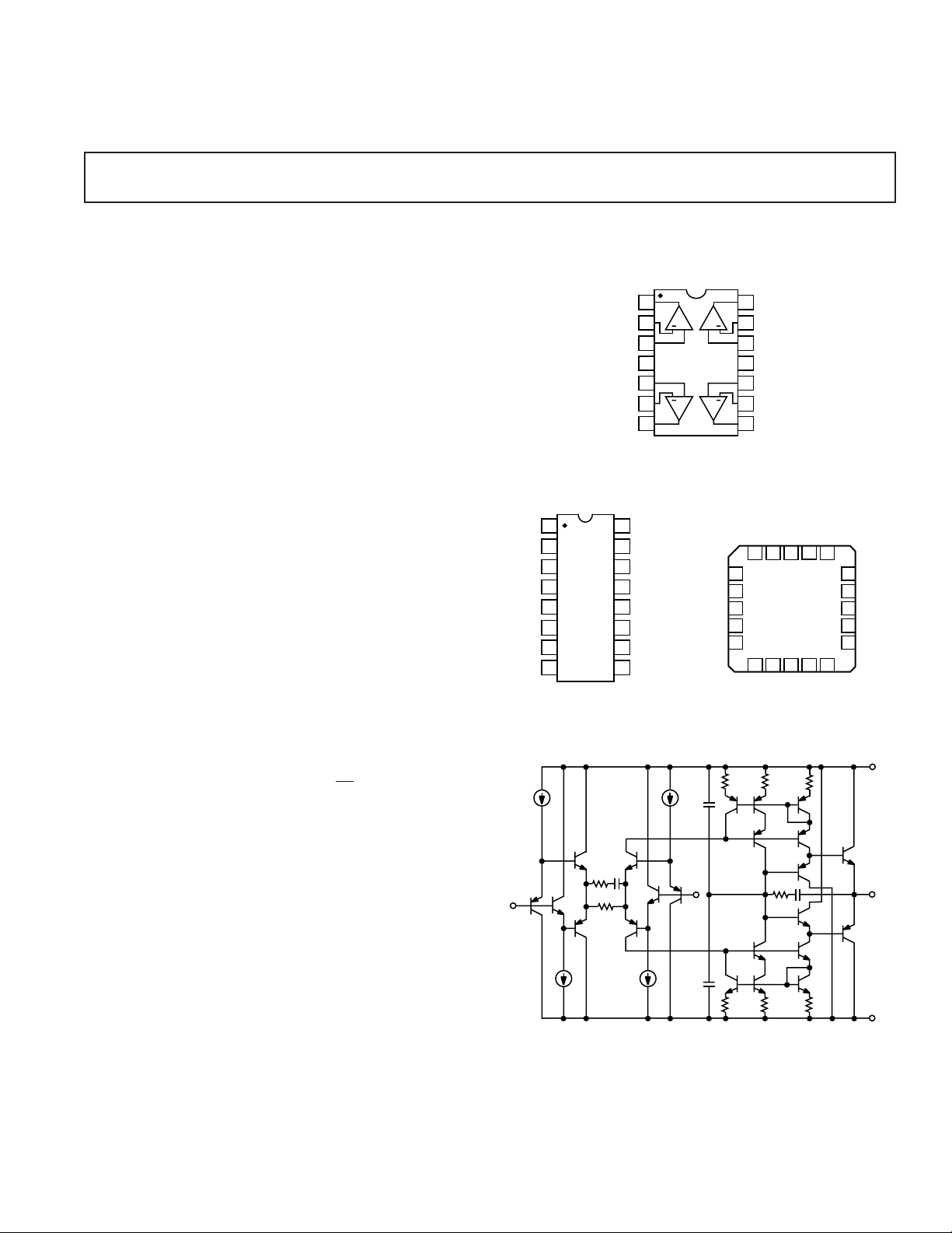
Quad Precision, High Speed
1
2
3
4
5
6
7
8
OUT A
–IN A
+IN A
V+
+IN B
–IN B
OUT B
16
15
14
13
12
11
10
9
OUT D
–IN D
+IN D
V–
+IN C
–IN C
OUT C
NC
NC
OP467
NC = NO CONNECT
a
FEATURES
High Slew Rate – 170 V/s
Wide Bandwidth – 28 MHz
Fast Settling Time – <200 ns to 0.01%
Low Offset Voltage – <500 V
Unity-Gain Stable
Low Voltage Operation ⴞ5 V to ⴞ15 V
Low Supply Current – <10 mA
Drives Capacitive Loads
APPLICATIONS
High Speed Image Display Drivers
High Frequency Active Filters
Fast Instrumentation Amplifiers
High Speed Detectors
Integrators
Photo Diode Preamps
GENERAL DESCRIPTION
The OP467 is a quad, high speed, precision operational amplifier. It offers the performance of a high speed op amp combined
with the advantages of a precision operational amplifier all in a
single package. The OP467 is an ideal choice for applications
where, traditionally, more than one op amp was used to achieve
this level of speed and precision.
The OP467’s internal compensation ensures stable unity-gain
operation, and it can drive large capacitive loads without oscillation. With a gain bandwidth product of 28 MHz driving a 30 pF
load, output slew rate in excess of 170 V/µs, and settling time to
0.01% in less than 200 ns, the OP467 provides excellent dynamic accuracy in high speed data-acquisition systems. The
channel-to-channel separation is typically 60 dB at 10 MHz.
The dc performance of OP467 includes less than 0.5 mV of
offset, voltage noise density below 6 nV/√
current under 10 mA. Common-mode rejection and power
supply rejection ratios are typically 85 dB. PSRR is maintained
to better than 40 dB with input frequencies as high as 1 MHz.
The low offset and drift plus high speed and low noise, make the
OP467 usable in applications such as high speed detectors and
instrumentation.
The OP467 is specified for operation from ±5 V to ±15 V over
the extended industrial temperature range (–40°C to +85°C) and
is available in 14-lead plastic and ceramic DIP, plus SOL-16
and 20-lead LCC surface mount packages.
Contact your local sales office for MIL-STD-883 data sheet and
availability.
Hz and total supply
16-Lead SOL
–IN
Operational Amplifier
PIN CONNECTIONS
14-Lead Ceramic DIP (Y Suffix) and
14-Lead Epoxy DIP (P Suffix)
OUT A
–IN A
+IN A
+IN B
–IN B
OUT B
(S Suffix)
1
2
+ +
3
4
V+
OP467
5
++
6
7
+IN
14
OUT D
13
–IN D
+IN D
12
11
V–
10
+IN C
9
–IN C
8
OUT C
20-Position Chip Carrier
(RC Suffix)
–IN A
3
4
+IN A
NC
5
OP467
6
V+
NC
+IN B
(TOP VIEW)
7
8
9
10 11
–IN B
NC = NO CONNECT
OP467
–IN D
NC
OUT A
OUT D
2012
19
12 13
NC
OUT C
–IN C
OUT B
+IN D
18
NC
17
16
V–
NC
15
14
+IN C
V+
OUT
V–
REV. C
Information furnished by Analog Devices is believed to be accurate and
reliable. However, no responsibility is assumed by Analog Devices for its
use, nor for any infringements of patents or other rights of third parties
which may result from its use. No license is granted by implication or
otherwise under any patent or patent rights of Analog Devices.
Figure 1. Simplified Schematic
One Technology Way, P.O. Box 9106, Norwood, MA 02062-9106, U.S.A.
Tel: 781/329-4700 World Wide Web Site: http://www.analog.com
Fax: 781/326-8703 © Analog Devices, Inc., 1998
Page 2
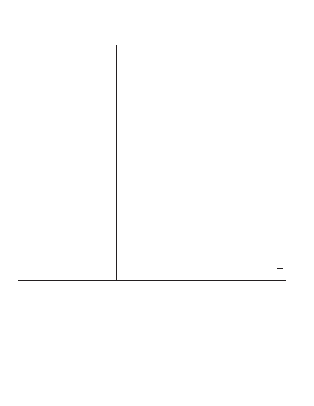
OP467–SPECIFICATIONS
ELECTRICAL CHARACTERISTICS
(@ VS = ⴞ15.0 V, TA = +25ⴗC unless otherwise noted)
Parameter Symbol Conditions Min Typ Max Units
INPUT CHARACTERISTICS
Offset Voltage V
Input Bias Current I
Input Offset Current I
OS
B
OS
Common-Mode Rejection CMR V
CMR V
Large Signal Voltage Gain A
Offset Voltage Drift ∆V
Bias Current Drift ∆I
VO
/∆T 3.5 µV/°C
OS
/∆T 0.2 pA/°C
B
–40°C ≤ T
≤ +85°C1mV
A
VCM = 0 V 150 600 nA
V
= 0 V, –40°C ≤ TA ≤ +85°C 150 700 nA
CM
VCM = 0 V 10 100 nA
V
= 0 V, –40°C ≤ TA ≤ +85°C 10 150 nA
CM
= ±12 V 80 90 dB
CM
= ±12 V, –40°C ≤ TA ≤ +85°C8088 dB
CM
R
= 2 kΩ 83 86 dB
L
R
= 2 kΩ, –40°C ≤ TA ≤ +85°C77.5 dB
L
0.2 0.5 mV
Long Term Offset Voltage Drift ∆VOS/∆T Note 1 750 µV
OUTPUT CHARACTERISTICS
R
Output Voltage Swing V
O
= 2 kΩ±13.0 ±13.5 V
L
R
= 2 kΩ, –40°C ≤ TA ≤ +85°C ±12.9 ±13.12 V
L
POWER SUPPLY
Power Supply Rejection Ratio PSRR ±4.5 V ≤ VS = ±18 V 96 120 dB
Supply Current I
Supply Voltage Range V
SY
–40°C ≤ T
VO = 0 V 8 10 mA
V
= 0 V, –40°C ≤ TA ≤ +85°C13mA
O
S
≤ +85°C 86 115 dB
A
±4.5 ±18 V
DYNAMIC PERFORMANCE
Gain Bandwidth Product GBP AV = +1, CL = 30 pF 28 MHz
Slew Rate SR V
Full-Power Bandwidth BW
Settling Time t
Phase Margin θ
ρ
S
0
= 10 V Step, R
IN
A
= +1 125 170 V/µs
V
A
= –1 350 V/µs
V
VIN = 10 V Step 2.7 MHz
To 0.01%, VIN = 10 V Step 200 ns
= 2 kΩ, C
L
= 30 pF
L
45 Degrees
Input Capacitance
Common Mode 2.0 pF
Differential 1.0 pF
NOISE PERFORMANCE
Voltage Noise e
Voltage Noise Density e
Current Noise Density i
NOTE
1
Long Term Offset Voltage Drift is guaranteed by 1000 hrs. Life test performed on three independent wafer lots at +125 °C, with an LTPD of 1.3.
Specifications subject to change without notice.
p-p f = 0.1 Hz to 10 Hz 0.15 µV p-p
N
N
N
f = 1 kHz 6 nV/√Hz
f = 1 kHz 8 pA/√Hz
–2–
REV. C
Page 3
OP467
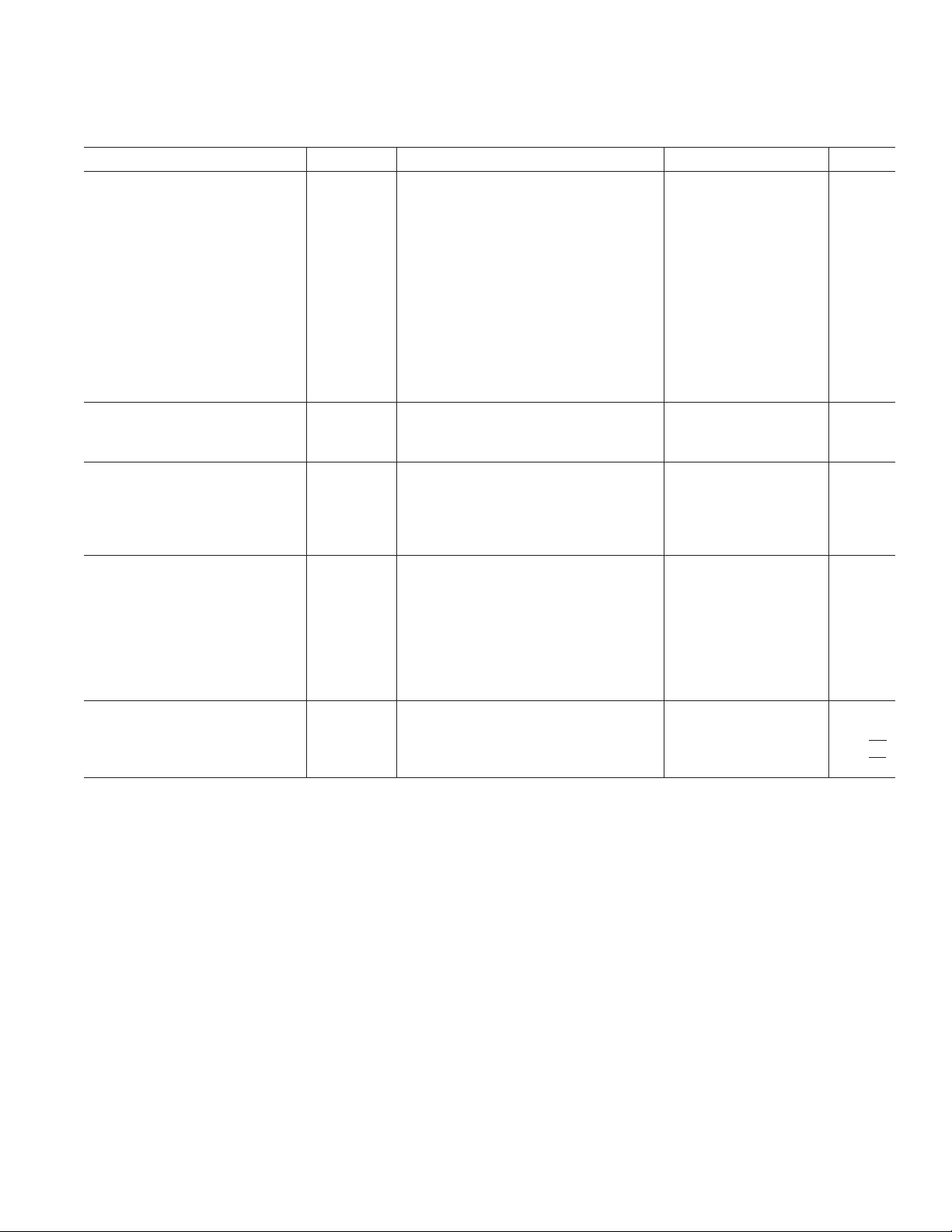
ELECTRICAL CHARACTERISTICS
(@ VS = ⴞ5.0 V, TA = +25ⴗC unless otherwise noted)
Parameter Symbol Conditions Min Typ Max Units
INPUT CHARACTERISTICS
Offset Voltage V
Input Bias Current I
Input Offset Current I
OS
B
OS
Common-Mode Rejection CMR V
CMR V
Large Signal Voltage Gain A
Offset Voltage Drift ∆V
VO
/∆T3 5µV/°C
OS
–40°C ≤ T
≤ +85°C1mV
A
VCM = 0 V 125 600 nA
V
= 0 V, –40°C ≤ TA ≤ +85°C 150 700 nA
CM
VCM = 0 V 20 100 nA
= 0 V, –40°C ≤ TA ≤ +85°C 150 nA
V
CM
= ±2.0 V 76 85 dB
CM
= ±2.0 V, –40°C ≤ TA ≤ +85°C76 80 dB
CM
R
= 2 kΩ 80 83 dB
L
R
= 2 kΩ, –40°C ≤ TA ≤ +85°C74 dB
L
0.3 0.5 mV
Bias Current Drift ∆IB/∆T 0.2 pA/°C
OUTPUT CHARACTERISTICS
Output Voltage Swing V
O
R
= 2 kΩ±3.0 ±3.5 V
L
R
= 2 kΩ, –40°C ≤ TA ≤ +85°C ±3.0 ±3.20 V
L
POWER SUPPLY
Power Supply Rejection Ratio PSRR ±4.5 V ≤ VS = ±5.5 V 92 107 dB
≤ +85°C 83 105 dB
A
Supply Current I
SY
–40°C ≤ T
VO = 0 V 8 10 mA
V
= 0 V, –40°C ≤ TA ≤ +85°C11mA
O
DYNAMIC PERFORMANCE
Gain Bandwidth Product GBP AV = +1 22 MHz
Slew Rate SR V
Full-Power Bandwidth BW
Settling Time t
Phase Margin θ
ρ
S
0
= 5 V Step, R
IN
A
= +1 90 V/µs
V
A
= –1 90 V/µs
V
VIN = 5 V Step 2.5 MHz
To 0.01%, VIN = 5 V Step 280 ns
= 2 kΩ, C
L
= 39 pF
L
45 Degrees
NOISE PERFORMANCE
Voltage Noise e
Voltage Noise Density e
Current Noise Density i
Specifications subject to change without notice.
p-p f = 0.1 Hz to 10 Hz 0.15 µV p-p
N
N
N
f = 1 kHz 7 nV/√Hz
f = 1 kHz 8 pA/√Hz
REV. C
–3–
Page 4
OP467
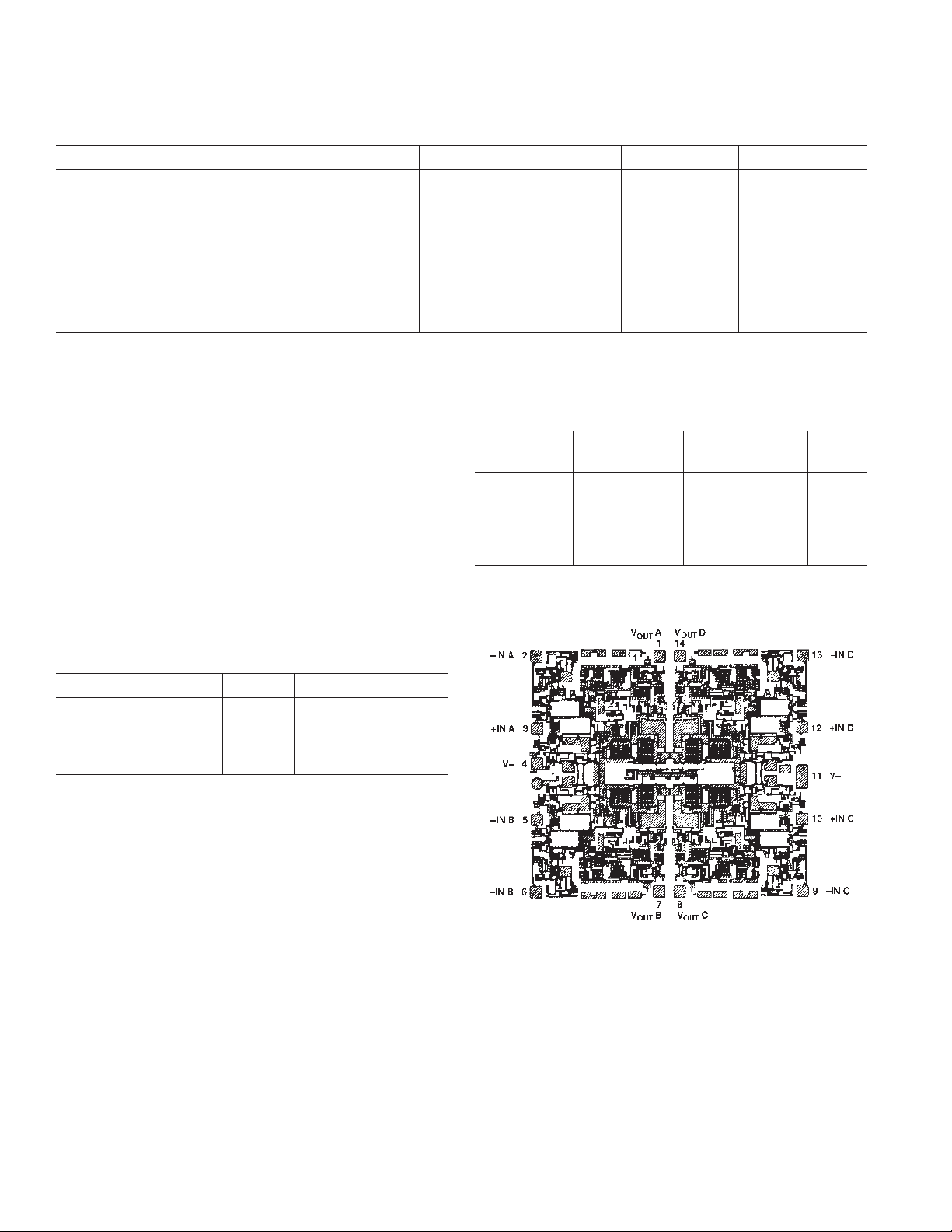
WAFER TEST LIMITS
1
( @ VS = ⴞ15.0 V, TA = +25ⴗC unless otherwise noted.)
Parameter Symbol Conditions Limit Units
Offset Voltage V
Input Bias Current I
Input Offset Current I
Input Voltage Range
2
OS
B
OS
Common-Mode Rejection Ratio CMRR V
VCM = 0 V 600 nA max
VCM = 0 V 100 nA max
= ±12 V 80 dB min
CM
±0.5 mV max
±12 V min/max
Power Supply Rejection Ratio PSRR V = ±4.5 V to ±18 V 96 dB min
R
Large Signal Voltage Gain A
Output Voltage Range V
Supply Current I
NOTES
1
Electrical tests and wafer probe to the limits shown. Due to variations in assembly methods and normal yield loss, yield after packaging is not guaranteed for standard
product dice. Consult factory to negotiate specifications based on dice lot qualifications through sample lot assembly and testing.
2
Guaranteed by CMR test.
ABSOLUTE MAXIMUM RATINGS
Supply Voltage . . . . . . . . . . . . . . . . . . . . . . . . . . . . . . . . ±18 V
Input Voltage
Differential Input Voltage
2
. . . . . . . . . . . . . . . . . . . . . . . . . . . . . . . . ±18 V
2
. . . . . . . . . . . . . . . . . . . . . . ±26 V
1
VO
O
SY
Output Short-Circuit Duration . . . . . . . . . . . . . . . . . . Limited
Storage Temperature Range
Y, RC Packages . . . . . . . . . . . . . . . . . . . . –65°C to +175°C
P, S Packages . . . . . . . . . . . . . . . . . . . . . . –65°C to +150°C
Operating Temperature Range
= 2 kΩ 83 dB min
L
R
= 2 kΩ±13.0 V min
L
VO = 0 V, R
= ∞ 10 mA max
L
ORDERING GUIDE
Temperature Package Package
Model Ranges Descriptions Options
OP467AY/883 –55°C to +125°C 14-Lead Cerdip Q-14
OP467ARC/883 –55°C to +125°C 20-Contact LCC E-20A
OP467GP –40°C to +85°C 14-Lead Plastic DIP N-14
OP467GS –40°C to +85°C 16-Lead SOL R-16
OP467GBC +25°C DICE
OP467A . . . . . . . . . . . . . . . . . . . . . . . . . . –55°C to +125°C
OP467G . . . . . . . . . . . . . . . . . . . . . . . . . . . –40°C to +85°C
Junction Temperature Range
DICE CHARACTERISTICS
Y, RC Packages . . . . . . . . . . . . . . . . . . . . –65°C to +175°C
P, S Packages . . . . . . . . . . . . . . . . . . . . . . –65°C to +150°C
Lead Temperature Range (Soldering, 60 sec) . . . . . . . +300°C
Package Type
3
A
JC
Units
14-Lead Cerdip (Y) 94 10 °C/W
14-Lead Plastic DIP (P) 76 33 °C/W
16-Lead SOL (S) 88 23 °C/W
20-Contact LCC (RC) 78 33 °C/W
NOTES
1
Absolute maximum ratings apply to both DICE and packaged parts, unless
otherwise noted.
2
For supply voltages less than ±18 V, the absolute maximum input voltage is equal
to the supply voltage.
3
θJA is specified for the worst case conditions, i.e., θ
for cerdip, P-DIP, and LCC packages; θ
board for SOIC package.
JA
is specified for device in socket
JA
is specified for device soldered in circuit
OP467 Die Size 0.111 ⫻ 0.100 inch, 11,100 sq. mils Substrate is Connected to V+, Number of Transistors 165.
–4–
REV. C
Page 5
0.0
100k 1M 10M
–0.1
–0.2
–0.3
0.1
0.2
0.3
GAIN ERROR – dB
FREQUENCY – Hz
3.4
5.8
VS = 65
VS = 615
Typical Performance Characteristics–
OP467
80
70
60
50
40
30
20
10
OPEN-LOOP GAIN – dB
0
–10
–20
1k 10k 100M10M1M100k
GAIN
PHASE
FREQUENCY – Hz
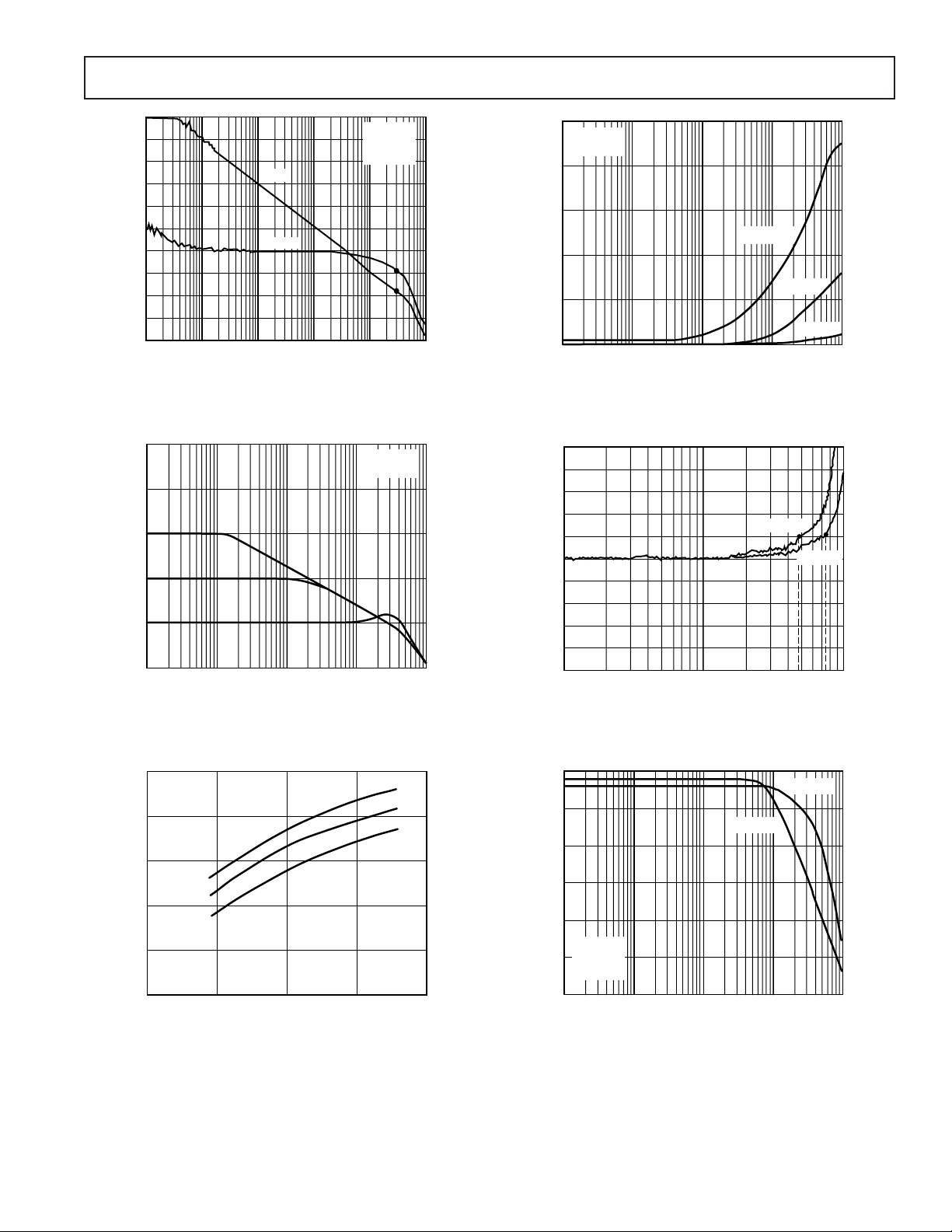
Figure 2. Open-Loop Gain, Phase vs. Frequency
80
60
40
VS = 615V
= 1MV
R
L
= 30pF
C
L
VS = 615V
T
= +258C
A
0
90
PHASE SHIFT – Degrees
180
100
VS = 615V
T
= +258C
A
80
60
A
= +100
VCL
40
IMPEDANCE – V
A
= +10
20
0
1k 100k10k100
FREQUENCY – Hz
VCL
A
= +1
VCL
1M
Figure 5. Closed-Loop Output Impedance vs. Frequency
20
CLOSED-LOOP GAIN – dB
0
–20
100k 100M10M1M10k
FREQUENCY – Hz
Figure 3. Closed-Loop Gain vs. Frequency
25
20
15
TA = +1258C
T
= +258C
A
10
= –558C
T
A
OPEN-LOOP GAIN – V/mV
5
0
0
65
SUPPLY VOLTAGE – Volts
Figure 4. Open-Loop Gain vs. Supply Voltage
Figure 6. Gain Linearity vs. Frequency
30
25
20
15
10
VS = 615V
MAXIMUM OUTPUT SWING – Volts
T
= +258C
5
A
R
= 2kV
L
615610
620
0
10k 10M1M100k1k
Figure 7. Max V
FREQUENCY – Hz
Swing vs. Frequency
OUT
A
VCL
= +1
A
= –1
VCL
REV. C
–5–
Page 6
OP467
p
12
VS = 65V
= +258C
T
A
= 2kV
R
10
L
8
6
4
MAXIMUM OUTPUT SWING – Volts
2
0
Figure 8. Max V
120
100
80
60
10k 10M1M100k1k
FREQUENCY – Hz
OUT
A
= +1
VCL
A
= –1
VCL
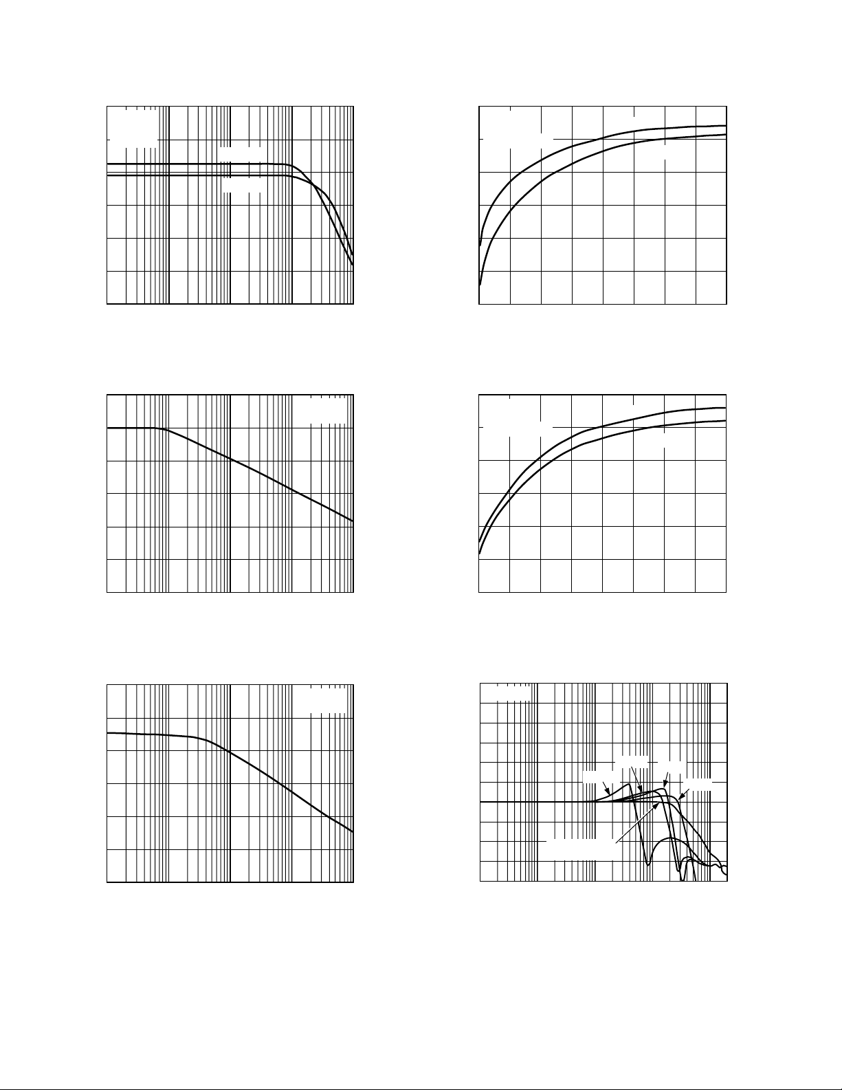
Swing vs. Frequency
VS = 615V
T
= +258C
A
60
VS = 615V
= 2kV
R
L
VIN = 100mV p-p
50
40
30
OVERSHOOT – %
20
10
0
200
0
LOAD CAPACITANCE – pF
A
= +1
VCL
A
= –1
VCL
1600
14001000800600 1200400
Figure 11. Small Signal Overshoot vs. Load Capacitance
60
VS = 65V
R
L
VIN = 100mV p-p
50
40
30
= 2kV
A
= +1
VCL
A
= –1
VCL
40
20
COMMON-MODE REJECTION – Volts
0
10k 10M1M100k1k
FREQUENCY – Hz
Figure 9. Common-Mode Rejection vs. Frequency
120
100
80
60
40
POWER SUPPLY REJECTION – dB
20
0
1k 1M100k10k100
FREQUENCY – Hz
VS = 615V
= +258C
T
A
Figure 10. Power-Supply Rejection vs. Frequency
OVERSHOOT – %
20
10
0
200
0
LOAD CAPACITANCE –
F
1600
14001000800600 1200400
Figure 12. Small Signal Overshoot vs. Load Capacitance
60
VS = 615V
50
40
30
10000pF
1000pF
500pF
200pF
20
10
GAIN – dB
0
–10
–20
–30
–40
10k 100M10M1M100k
CIN = NETWORK
ANALYZER
FREQUENCY – Hz
Figure 13. Noninverting Gain vs. Capacitive Loads
–6–
REV. C
Page 7
OP467
0
VS = 615V
–10
–20
–30
–40
–50
–60
–70
CHANNEL SEPARATION – dB
–80
–90
–100
100 1k 100M10M1M100k10k
FREQUENCY – Hz
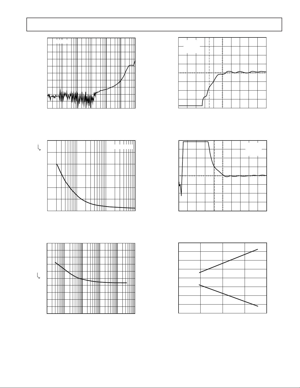
Figure 14. Channel Separation vs. Frequency
12
65V # VS # 15V
10
8
6
4
2
INPUT CURRENT NOISE DENSITY – pA/ Hz
0
FREQUENCY – Hz
10011k10
Figure 15. Input Current Noise Density vs. Frequency
4
VS = 615V
V
= 65V
3
IN
C
= 50pF
L
2
1
0
ERROR – mV
–1
OUT
V
–2
–3
–4
0
TIME – ns
Figure 17. Settling Time, Negative Edge
4
3
2
1
0
ERROR – mV
–1
OUT
V
–2
–3
–4
0
TIME – ns
Figure 18. Settling Time, Positive Edge
400300200100
VS = 615V
= 65V
V
IN
= 50pF
C
L
400300200100
500
500
100
10
nV/ Hz
1.0
0.1 1 10k1k10010
FREQUENCY – Hz
Figure 16. Voltage Noise Density vs. Frequency
REV. C
–7–
20
TA = +258C
15
10
5
0
–5
–10
INPUT VOLTAGE RANGE – Volts
–15
–20
SUPPLY VOLTAGE – Volts
615610
620650
Figure 19. Input Voltage Range vs. Supply Voltage
Page 8
OP467
50
VS1 = 615V
40
V
= 65V
S2
R
= 10kV
L
30
C
= 50pF
L
20
10
0
GAIN – dB
–10
–20
–30
–40
–50
100k 100M10M1M10k
FREQUENCY – Hz
VS2 = 65V
VS1 = 615V
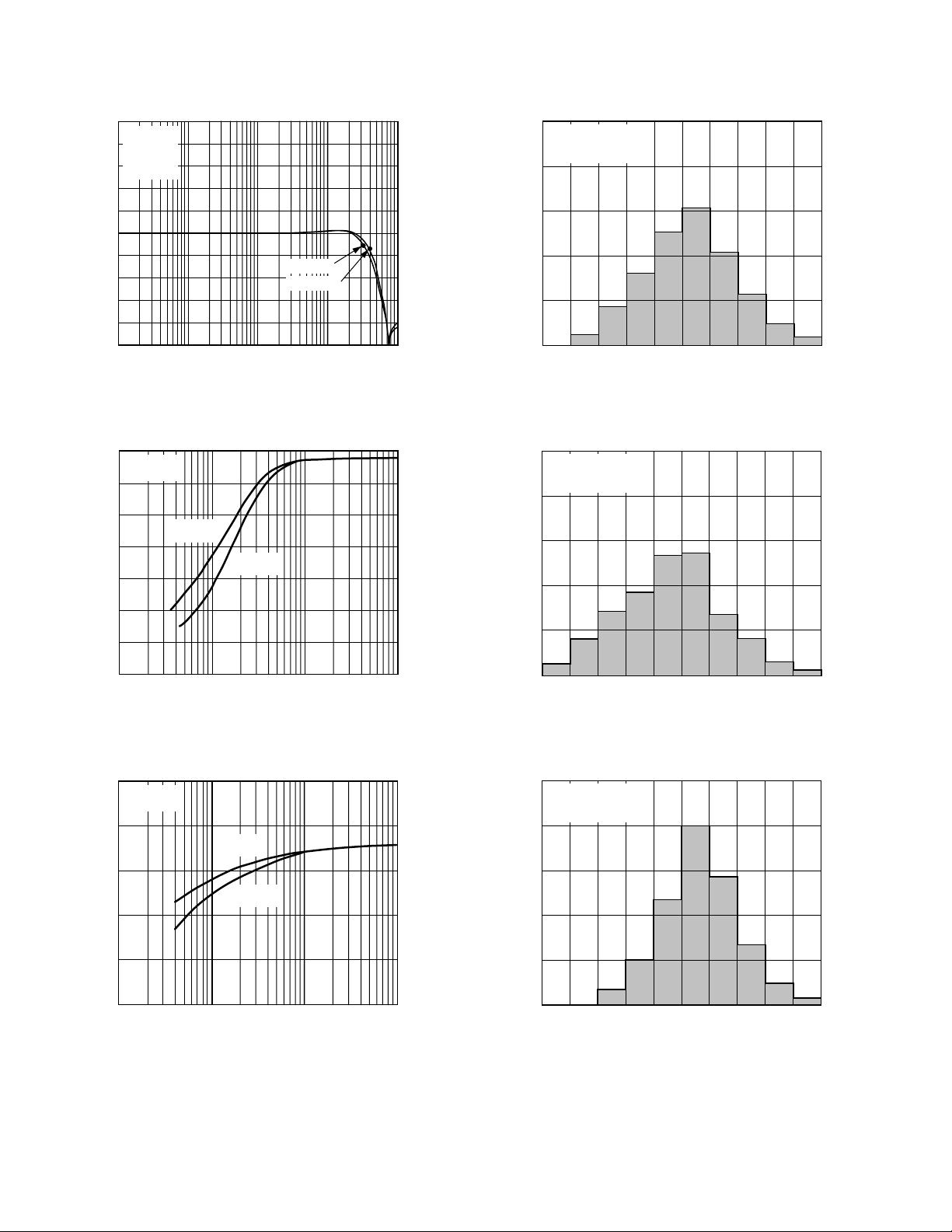
Figure 20. Noninverting Gain vs. Supply Voltage
14
VS = 615V
= +258C
T
A
12
10
8
6
4
OUTPUT SWING – Volts
2
POSITIVE
SWING
NEGATIVE
SWING
500
VS = 615V
= +258C
T
A
1252 3 OP AMPS
400
300
UNITS
200
100
0
–50
–100
INPUT OFFSET VOLTAGE – VOS mV
350300250200150100500
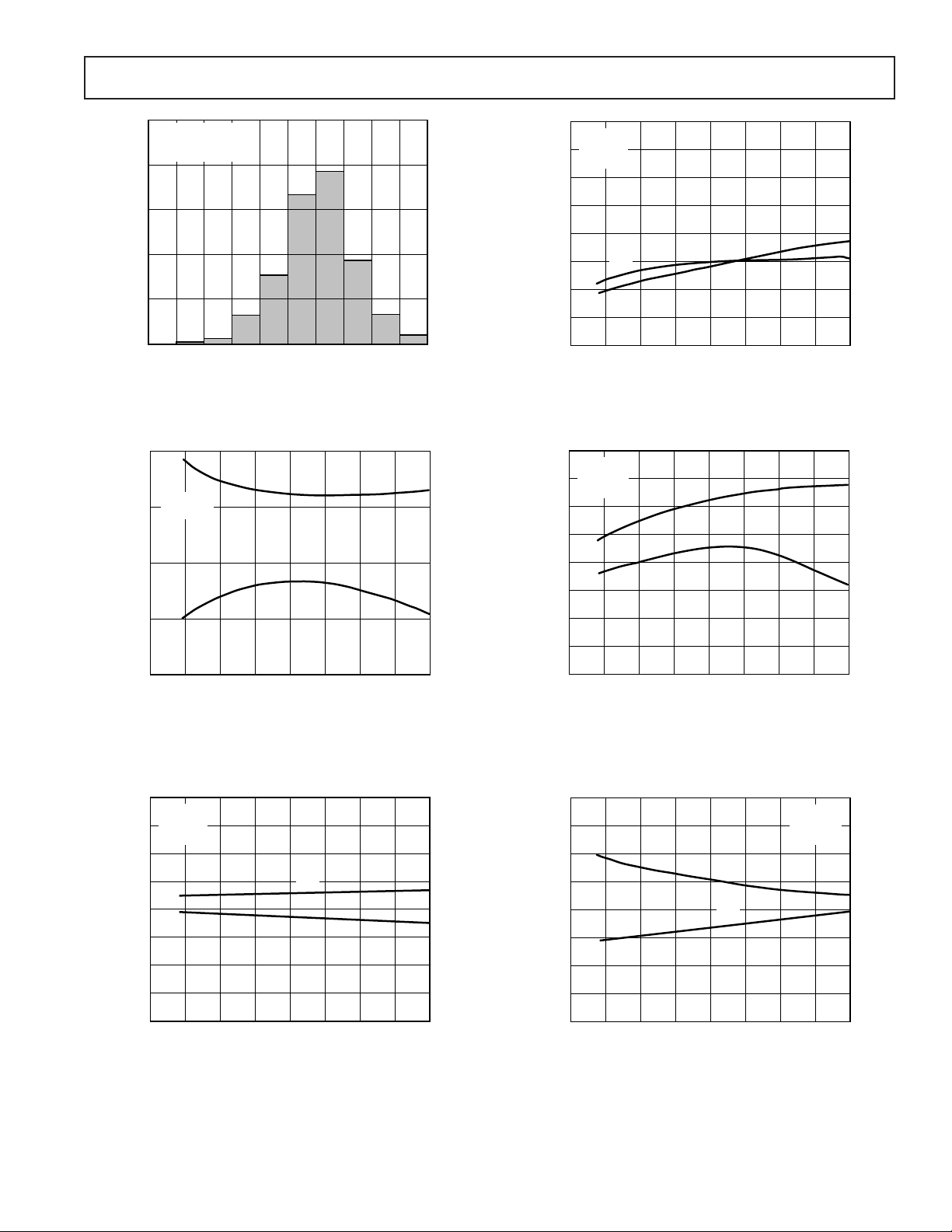
Figure 23. Input Offset Voltage Distribution
500
VS = 65V
= +258C
T
A
1252 3 OP AMPS
400
300
UNITS
200
100
400
0
100 10k1k10
LOAD RESISTANCE – V
Figure 21. Output Swing vs. Load Resistance
5
VS = 65V
T
= +258C
A
4
3
2
OUTPUT SWING – Volts
1
0
POSITIVE
SWING
NEGATIVE
SWING
100 10k1k10
LOAD RESISTANCE – V
Figure 22. Output Swing vs. Load Resistance
0
–50
–100
INPUT OFFSET VOLTAGE – VOS mV
350300250200150100500
Figure 24. Input Offset Voltage Distribution
500
VS = 615V
= +258C
T
A
1252 3 OP AMPS
400
300
UNITS
200
100
0
0.5
0
TC VOS – mV/8C
4.54.03.53.02.52.01.51.0
Figure 25. TC VOS Distribution
400
5.0
–8–
REV. C
Page 9
OP467
500
400
300
UNITS
200
100
60
55
50
0
0
VS = 65V
= +258C
T
A
1252 3 OP AMPS
0.5
TC VOS – mV/8C
Figure 26. TC VOS Distribution
VS = 615V
= 2kV
R
L
GBW
400
VS = 65V
R
= 2kV
L
350
300
s
m
250
200
150
SLEW RATE – V/
100
50
5.0
4.54.03.53.02.52.01.51.0
= +1
A
VCL
+SR
–SR
0
–50–75
TEMPERATURE – 8C
125
1007550250–25
Figure 29. Slew Rate vs. Temperature
29.0
28.5
28.0
650
VS = 615V
= 2kV
R
600
L
= –1
A
VCL
550
s
m
500
450
–SR
+SR
FM
45
PHASE MARGIN – Degrees
40
–75 125
–50
TEMPERATURE – 8C
75 10050250–25
Figure 27. Phase Margin and Gain Bandwidth vs.
Temperature
400
VS = 65V
= 2kV
R
L
350
300
250
200
150
SLEW RATE – V/ms
100
50
= –1
A
VCL
–SR
+SR
0
–50–75
TEMPERATURE – 8C
Figure 28. Slew Rate vs. Temperature
400
SLEW RATE – V/
27.5
27.0
GAIN BANDWIDTH PRODUCT – MHz
350
300
250
1007550250–25
–50–75
TEMPERATURE – 8C
125
Figure 30. Slew Rate vs. Temperature
400
350
300
s
m
250
200
150
SLEW RATE – V/
100
50
125
1007550250–25
0
–50–75
TEMPERATURE – 8C
+SR
–SR
VS = 615V
R
= 2kV
L
= +1
A
VCL
1007550250–25
125
Figure 31. Slew Rate vs. Temperature
REV. C
–9–
Page 10
OP467
10
–2
–4
–6
–8
OUTPUT STEP FOR 615V SUPPLY – Volts
–10
RF = 5kV
T
= +258C
8
A
6
4
2
0
0
0.1%
100
SETTLING TIME – ns
0.01%
0.1% 0.01%
300200
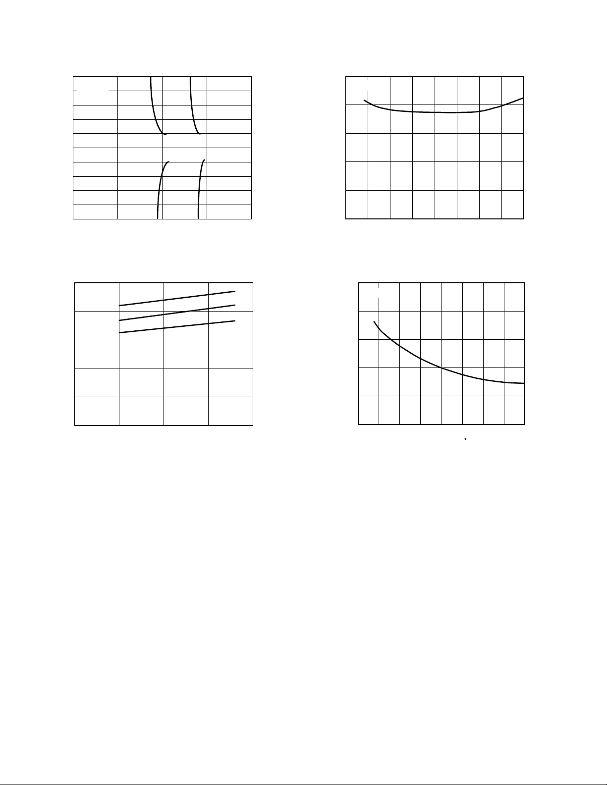
Figure 32. Settling Time vs. Output Step
10
TA = +1258C
8
= +258C
T
A
T
= –558C
A
6
400
5
4
3
2
1
0
–5
–4
–3
–2
–1
OUTPUT STEP FOR 65V SUPPLY – Volts
200
VS = 615V
160
120
80
INPUT BIAS CURRENT – nA
40
0
–50
–75
TEMPERATURE –
8
C
1007550250–25
125
Figure 34. Input Bias Current vs. Temperature
25
VS = 615V
20
15
4
SUPPLY CURRENT – mA
2
0
0
65
SUPPLY VOLTAGE – Volts
615610
620
Figure 33. Supply Current vs. Supply Voltage
10
INPUT OFFSET CURRENT – nA
5
0
–75
–50
TEMPERATURE –
C
125
1007550250–25
Figure 35. Input Offset Current vs. Temperature
–10–
REV. C
Page 11
OP467
APPLICATIONS INFORMATION
OUTPUT SHORT-CIRCUIT PERFORMANCE
To achieve a wide bandwidth and high slew rate, the OP467
output is not short circuit protected. Shorting the output to
ground or to the supplies may destroy the device.
For safe operation, the output load current should be limited so
that the junction temperature does not exceed the absolute
maximum junction temperature.
To calculate the maximum internal power dissipation, the following formula can be used:
TT
max
–
J
P
=
D
A
θ
A
J
where TJ and TA are junction and ambient temperatures respectively, P
is device internal power dissipation, and θ
D
is pack-
JA
aged device thermal resistance given in the data sheet.
UNUSED AMPLIFIERS
It is recommended that any unused amplifiers in a quad package
be connected as a unity gain follower with a 1 kΩ feedback
resistor with noninverting input tied to the ground plain.
PRINTED CIRCUIT BOARD LAYOUT
CONSIDERATIONS
Satisfactory performance of a high speed op amp largely depends
on a good PC layout. To achieve the best dynamic performance,
following high frequency layout technique is recommended.
GROUNDING
A good ground plain is essential to achieve the optimum performance in high speed applications. It can significantly reduce the
undesirable effects of ground loops and IR drops by providing a
low impedance reference point. Best results are obtained with a
multilayer board design with one layer assigned to ground plain.
To maintain a continuous and low impedance ground, avoid
running any traces on this layer.
POWER SUPPLY CONSIDERATIONS
In high frequency circuits, device lead length introduces an
inductance in series with the circuit. This inductance, combined
with stray capacitance, forms a high frequency resonance circuit.
Poles generated by these circuits will cause gain peaking and
additional phase shift, reducing the op amp’s phase margin and
leading to an unstable operation.
A practical solution to this problem is to reduce the resonance
frequency low enough to take advantage of the amplifier’s power
supply rejection.
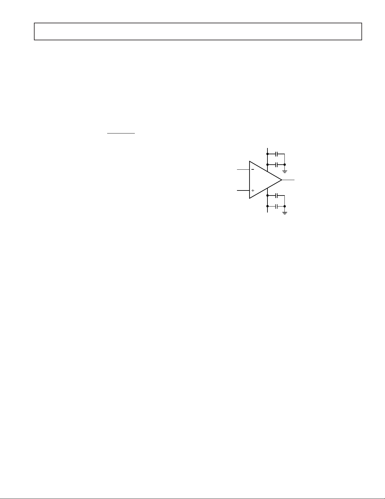
This is easily done by placing capacitors across the supply line
and the ground plain as close as possible to the device pin. Since
capacitors also have internal parasitic components, such as stray
inductance, selecting the right capacitor is important. To be
effective, they should have low impedance over the frequency
range of interest. Tantalum capacitors are an excellent choice
for their high capacitance/size ratio, but their ESR (Effective
Series Resistance) increases with frequency making them less
effective. On the other hand, ceramic chip capacitors have excellent ESR and ESL (Effective Series Inductance) performance at
higher frequencies, and because of their small size, they can be
placed very close to the device pin, further reducing the stray
inductance. Best results are achieved by using a combination of
these two capacitors. A 5 µF–10 µF tantalum parallel with a
0.1 µF ceramic chip caps are recommended. If additional isola-
tion from high frequency resonances of the power supply is
needed, a ferrite bead should be placed in series with the supply
lines between the bypass caps and the power supply. A word of
caution, addition of the ferrite bead will introduce a new pole
and zero to frequency response of the circuit and could cause
unstable operation if it is not selected properly.
+V
S
+
10mF TANTALUM
0.1mF CERAMIC CHIP
0.1mF CERAMIC CHIP
10mF TANTALUM
–
–V
S
Figure 36. Recommended Power Supply Bypass
SIGNAL CONSIDERATIONS
Input and output traces need special attention to assure a minimum stray capacitance. Input nodes are very sensitive to capacitive reactance, particularly when connected to a high impedance
circuit. Stray capacitance can inject undesirable signals from a
noisy line into a high impedance input. Protect high impedance
input traces by providing guard traces around them. This will
also improve the channel separation significantly.
Additionally, any stray capacitance in parallel with the op amp’s
input capacitance generates a pole in the frequency response of
the circuit. The additional phase shift caused by this pole will
reduce the circuit’s gain margin. If this pole is within the gain
range of the op amp, it will cause unstable performance. To
reduce these undesirable effects, use the lowest impedance
where possible. Lowering the impedance at this node places the
poles at a higher frequency, far above the gain range of the amplifier. Stray capacitance on the PC board can be reduced by
making the traces narrow and as short as possible. Further reduction can be realized by choosing smaller pad size, increasing
the spacing between the traces, and using PC board material
with a low dielectric constant insulator (Dielectric Constant of
some common insulators: air = 1, Teflon
®
= 2.2, and FR4 =
4.7; with air being an ideal insulator).
Removing segments of the ground plain directly under the input
and output pads is recommended.
Outputs of high speed amplifiers are very sensitive to capacitive
loads. A capacitive load will introduce a pair of pole and zero to
the circuit’s frequency response, reducing the phase margin,
leading to unstable operation or oscillation.
Teflon is a registered trademark of E.I. du Pont Co.
REV. C
–11–
Page 12
OP467
Generally, it is a good design practice to isolate the amplifier’s
output from any capacitive load by placing a resistor between
the amplifier’s output and the rest of the circuits. A series resistor of 10 to 100 ohms is normally sufficient to isolate the output
from a capacitive load.
The OP467 is internally compensated to provide stable operation, and is capable of driving large capacitive loads without
oscillation.
Sockets are not recommended since they increase the lead inductance/capacitance and reduce the power dissipation of the
package by increasing the leads thermal resistance. If sockets
must be used, use Teflon or pin sockets with the shortest leads
possible.
PHASE REVERSAL
The OP467 is immune to phase reversal; its inputs can exceed
the supply rails by a diode drop without any phase reversal.
15.8V
D
V1
100
90
OUTPUT
INPUT
10
0%
10V 10V
200ms
DLY 4.806ms
100
90
10
0%
5V
5V
20ns
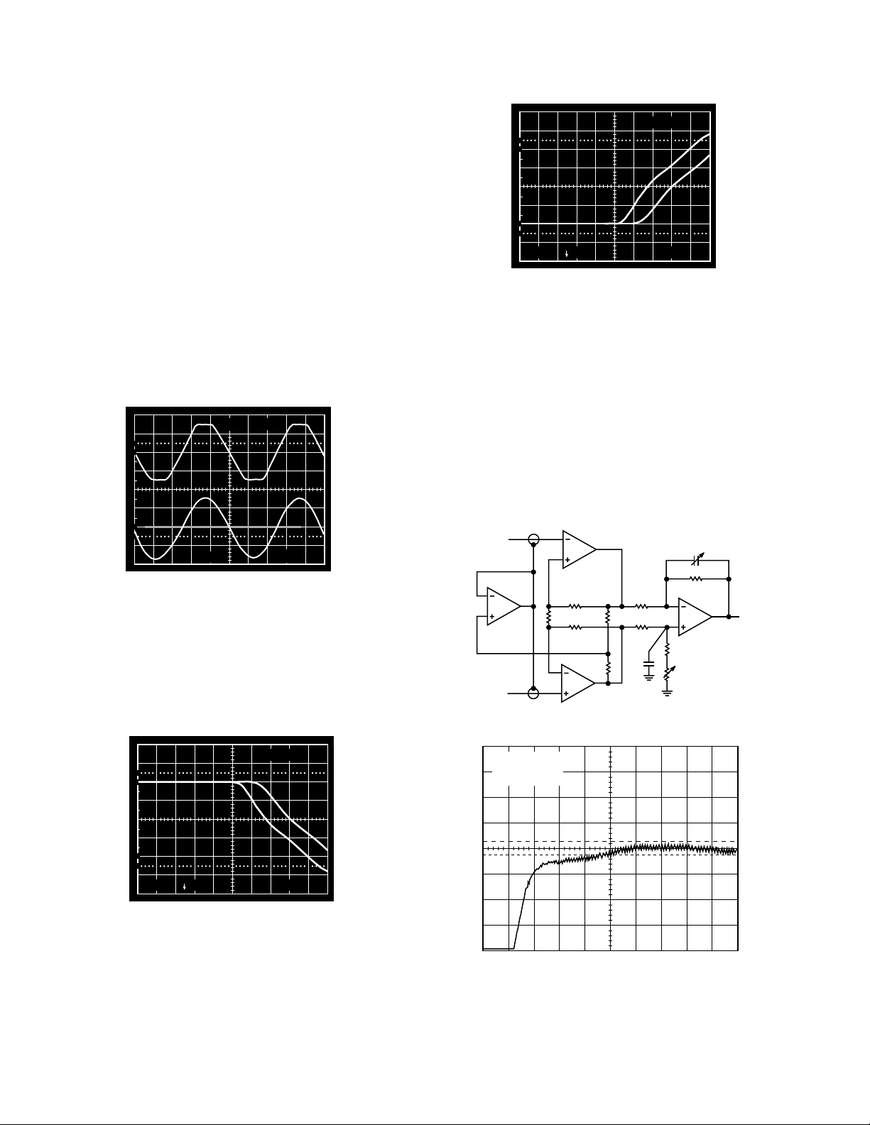
Figure 39. Saturation Recovery Time, Negative Rail
HIGH SPEED INSTRUMENTATION AMPLIFIER
The OP467 performance lends itself to a variety of high speed
applications, including high speed precision instrumentation
amplifiers. Figure 40 represents a circuit commonly used for
data acquisition, CCD imaging and other high speed application.
Circuit gain is set by R
to 2; for unity gain, remove R
. A 2 kΩ resistor will set the circuit gain
G
. For any other gain settings use
G
the following formula:
G = 2/R
R
is used for adjusting the dc common-mode rejection, and C
C
Resistor Value is in kΩ
G
C
is used for ac common-mode rejection adjustments.
–V
IN
C
C
Figure 37. No Phase Reversal (AV = +1)
SATURATION RECOVERY TIME
The OP467 has a fast and symmetrical recovery time from either rail. This feature is very useful in applications such as high
speed instrumentation and measurement circuits, where the
amplifier is frequently exposed to large signals that overload the
amplifier.
DLY 9.842ms
100
90
10
0%
5V
5V
20ns
Figure 38. Saturation Recovery Time, Positive Rail
1.9kV
R
C
200
10T
2kV
OUTPUT
V
1kV
10kV
R
G
1kV
10kV
+V
IN
2kV
2kV
5pF
Figure 40. A High Speed Instrumentation Amplifier
0.01% 10V STEP
VS = 615V
NEG SLOPE
2.5mV
–2.5mV
Figure 41. Instrumentation Amplifier Settling Time to
0.01% for a 10 V Step Input (Negative Slope)
–12–
REV. C
Page 13
OP467
2kV
R1
3kV
V
IN
R3
2kV
R2
2kV
R4
2kV
R5
2kV
C2
50pF
C1
50pF
R6
1kV
V
OUT
+
–
+
–
+
–
+
–
1/4
OP467
1/4
OP467
1/4
OP467
1/4
OP467
0.01% 10V STEP
VS = 615V
POS SLOPE
2.5mV
–2.5mV
Figure 42. Instrumentation Amplifier Settling Time to
0.01% for a 10 V Step Input (Positive Slope)
+V
S
+
–V
+
AD9617
–
–
S
549V
1kV
ERROR
TO
SCOPE
INPUT
IN-AMP
OUTPUT
TO
TO
2kV
2kV
61.9V
2 MHz BIQUAD BANDPASS FILTER
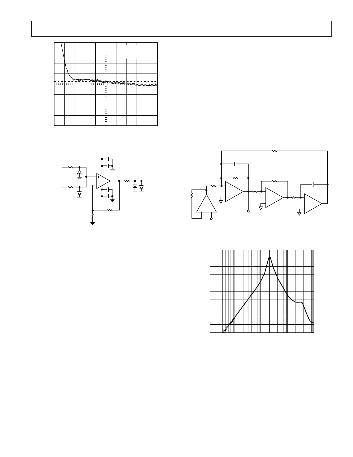
The circuit in Figure 44 is commonly used in medical imaging
ultrasound receivers. The 30 MHz bandwidth is sufficient to
accurately produce the 2 MHz center frequency, as the measured response shows in Figure 45. When the op amp’s bandwidth is too close to the filter’s center frequency, the amplifier’s
internal phase shift causes excess phase shift at 2 MHz, which
alters the filter’s response. In fact, if the chosen op amp has a
bandwidth close to 2 MHz, the combined phase shift of the
three op amps will cause the loop to oscillate.
Careful consideration must be given to the layout of this circuit
as with any other high speed circuit.
If the phase shift introduced by the layout is large enough, it
could alter the circuit performance, or worse, it will oscillate.
Figure 43. Settling Time Measurement Circuit
REV. C
Figure 44. 2 MHz Biquad Filter
0
–10
–20
GAIN – dB
–30
–40
100k 100M10M1M10k
FREQUENCY – Hz
Figure 45. Biquad Filter Response
–13–
Page 14
OP467
+5V
V
1
2
3
4
5
6
7
8
9
10
11
12
13
14
DD
DAC8408
V
A
REF
R
A
FB
1A
I
OUT
2A/
I
OUT
I
2B
OUT
I
1B
OUT
B
R
FB
V
B
REF
DB0 (LSB)
DB1
DB2
DB3
DB4
DB5
(MSB) DB7
+10V
C1
10pF
2
V
A
OUT
0.1mF
V
B
OUT
0.1mF
1
7
OP467
+15V
4
OP467
11
–15V
–
3
+
6
–
+
C2
+10V
10pF
5
Figure 46. Quad DAC Unipolar Operation
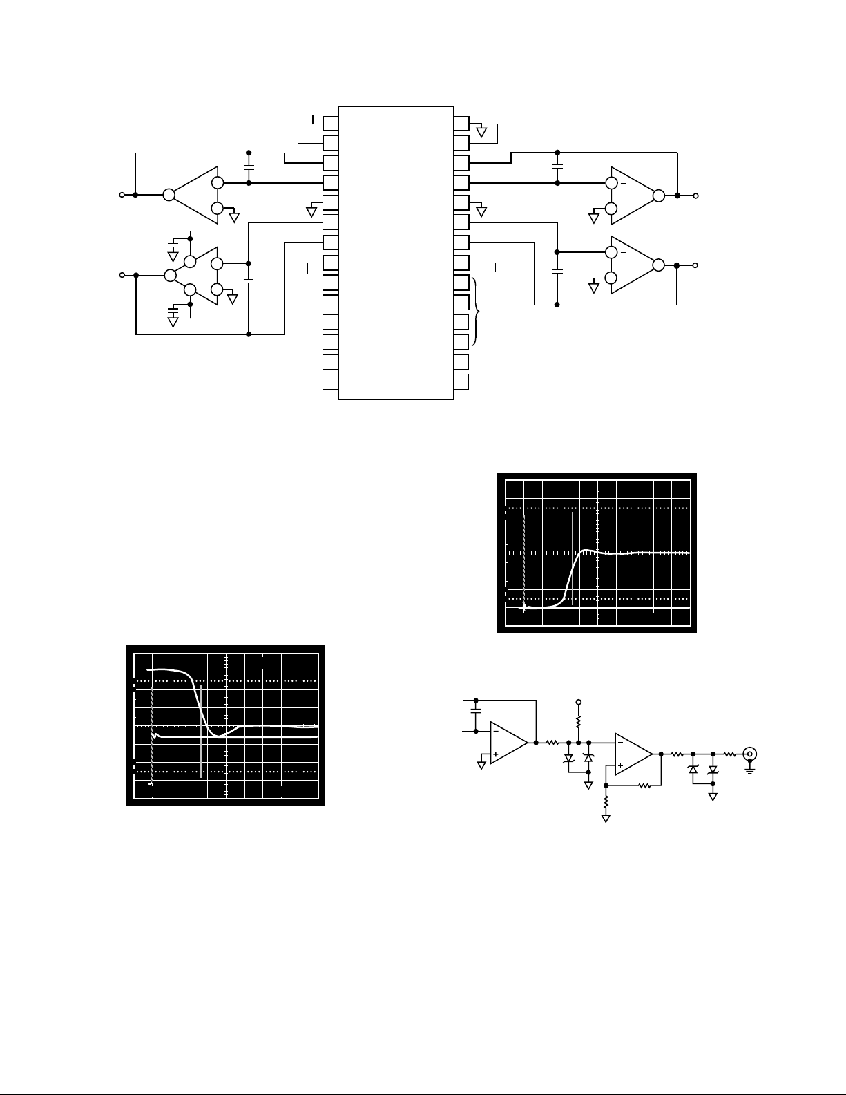
FAST I-TO-V CONVERTER
The fast slew rate and fast settling time of the OP467 are well
suited to the fast buffers and I-to-V converters used in variety of
applications. The circuit in Figure 46 is a unipolar quad D/A
converter consisting of only two ICs. The current output of the
DAC8408 is converted to a voltage by the OP467 configured as
an I-to-V converter. This circuit is capable of settling to 0.1%
within 200 ns. Figures 47 and 48 show the full-scale settling
time of the outputs. To obtain reliable circuit performance, keep
the traces from the DAC’s I
to the inverting inputs of the
OUT
OP467 short to minimize parasitic capacitance.
I
I
OUT
OUT
I
OUT
I
OUT
DGND
V
REF
R
FB
2C/
R
FB
V
REF
DS2
DS1
R/W
A/B
DB6
1C
2D
1D
+10V
28
C
27
C
26
25
24
23
22
D
D
21
+10V
20
19
DIGITAL
CONTROL
SIGNALS
18
17
16
15
100
90
10
0%
2V 50mV
C3
10pF
C4
10pF
13
12
9
10
OP467
+
OP467
+
251.0ns
100ns
V
14
8
A
OUT
V
B
OUT
260.0ns
100
90
10
0%
2V 50mV
100ns
Figure 47. Voltage Output Settling Time
Figure 48. Voltage Output Settling Time
DAC-8408
R
FB
3pF
I
OUT
Figure 49. DAC V
I-V
OP467
DC OFFSET
2kV
2kV
AD847
60.4V
Settling Time Circuit
OUT
604V
1kV
50V
–14–
REV. C
Page 15
OP467
OP467 SPICE MACRO-MODEL
* Node assignments
noninverting input
inverting input
positive supply
negative supply
output
*
. SUBCKT OP467 1 2 99 50 27
*
* INPUT STAGE
*
I1 4 50 10E–3
CIN 1 2 1E–12
IOS 1 2 5E–9
Q1 528 QN
Q2 679 QN
R3 99 5 185 . 681
R4 99 6 185 . 681
R5 8 4 180 . 508
R6 9 4 180 . 508
EOS 7 1 POLY (1) (14,20) 50E–6 1
EREF 98 0 (20,0) 1
*
* GAIN STAGE AND DOMINANT POLE AT 1.5 kHz
*
R7 10 98 3 . 714E6
C2 10 98 28 . 571E–12
G1 98 10 (5,6) 5 . 386E–3
V1 99 11 1 . 6
V2 12 50 1 . 6
D1 10 11 DX
D2 12 10 DX
RC 10 28 1 . 4E3
CC 28 27 12E–12
*
* COMMON-MODE STAGE WITH ZERO AT 1.26 kHz
*
ECM 13 98 POLY (2) (1,20) (2,20) 0 0 . 5 0 . 5
R8 13 14 1E6
R9 14 98 25 . 119
C3 13 14 126 . 721E–12
*
* POLE AT 400E6
*
R10 15 98 1E6
C4 15 98 0 . 398E–15
G2 98 15 (10,20) 1E–6
*
* OUTPUT STAGE
*
ISY 99 50 –8 . 183E–3
RMP1 99 20 96 . 429E3
RMP2 20 50 96 . 429E3
RO1 99 26 200
RO2 26 50 200
L1 26 27 1E–7
GO1 26 99 (99,15) 5E–3
GO2 50 26 (15,50) 5E–3
G4 23 50 (15,26) 5E–3
G5 24 50 (26,15) 5E–3
V3 21 26 50
V4 26 22 50
D3 15 21 DX
D4 22 15 DX
D5 99 23 DX
D6 99 24 DX
D7 50 23 DY
D8 50 24 DY
*
* MODELS USED
*
. MODEL QN NPN (BF=33.333E3)
. MODEL DX D
. MODEL DY D (BV=50)
. ENDS OP467
99
R10
G2
E
REF
50
REV. C
I
SY
15
C4
98
+
–
RMP1
20
RMP2
G4
D5
D6
V3
+
21
D3
15
D4
22
23
D7
–
V4
+
–
24
D8
G5
G01
R01
26
R02
G02
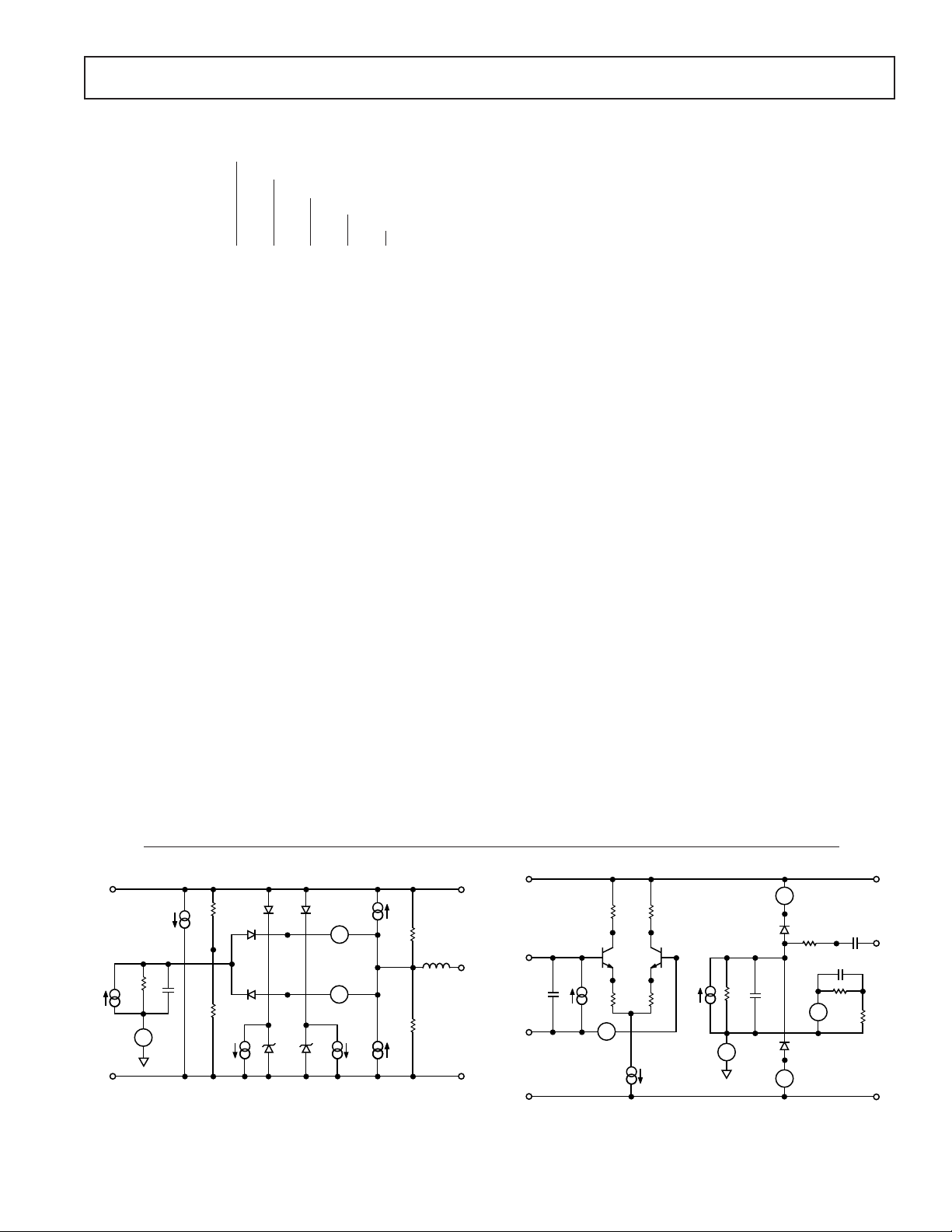
Figure 50. SPICE Macro-Model Output Stage
99
L1
27
50
99
+
–
V1
11
D1
R
10
R7
C2
98
+
–
V2
C
13
+
–
E
CM
D2
12
+
–
Q1
R4
6
Q2
7
G1
R6
4
+
E
REF
I1
R3
5
2
N–
89
I
OS
C
IN
1
N+
50
R5
–
E
OS
99
C
C
27
28
C3
14
R8
R9
50
Figure 51. SPICE Macro-Model Input and Gain Stage
–15–
Page 16
OP467
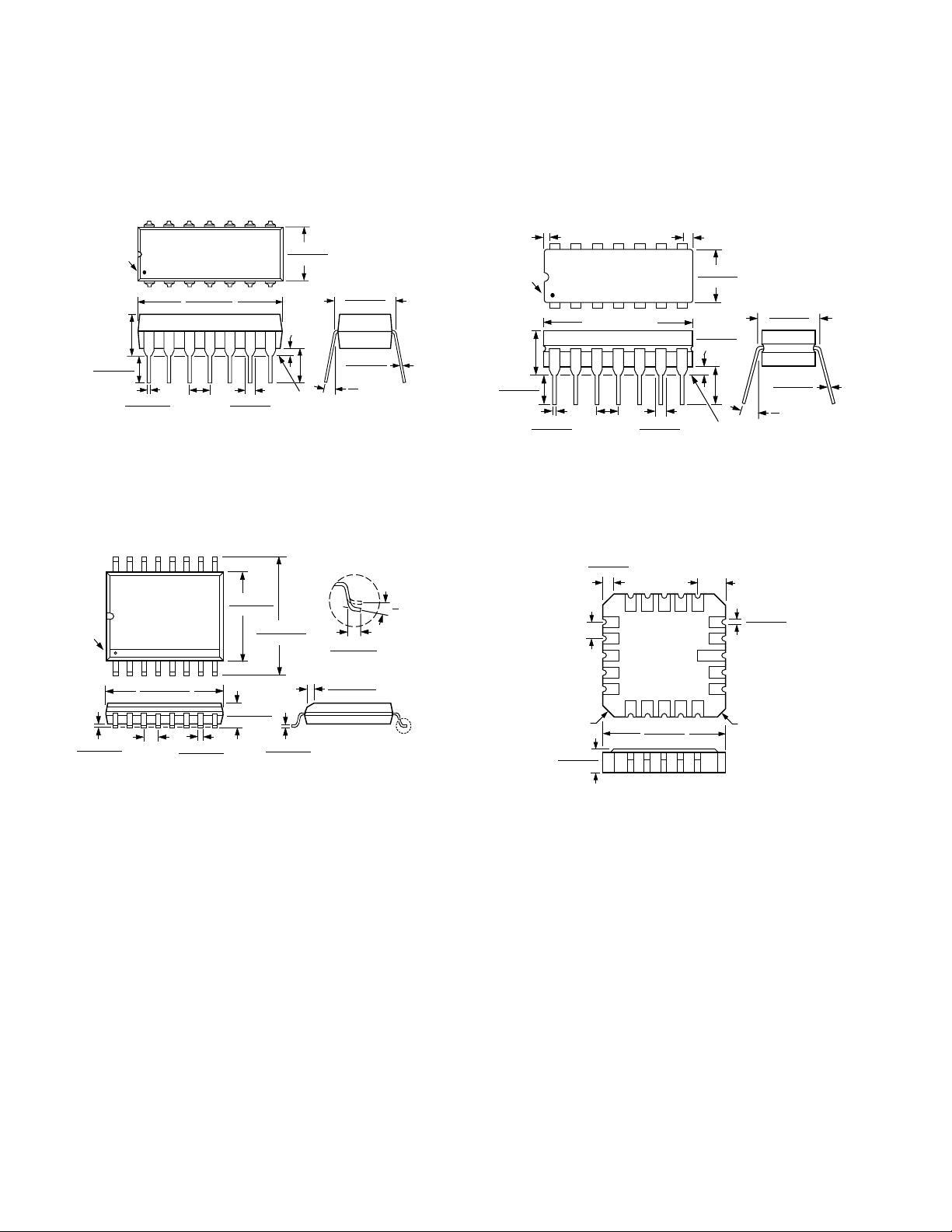
OUTLINE DIMENSIONS
Dimensions shown in inches and (mm).
(5.33)
0.160 (4.06)
0.115 (2.92)
PIN 1
0.0118 (0.30)
0.0040 (0.10)
14-Lead Plastic DIP (P Suffix)
(N-14)
814
7
0.280 (7.11)
0.240 (6.10)
0.015
(0.381)
MIN
0.130
(3.30)
MIN
SEATING
PLANE
PIN 1
0.210
MAX
0.022 (0.558)
0.014 (0.36)
1
0.795 (20.19)
0.725 (18.42)
0.100
0.070 (1.77)
(2.54)
0.045 (1.15)
BSC
16-Lead Wide-Body SOL (S Suffix)
(R-16)
0.0192 (0.49)
0.0138 (0.35)
9
0.2992 (7.60)
0.2914 (7.40)
8
0.1043 (2.65)
0.0926 (2.35)
0.4193 (10.65)
0.3937 (10.00)
0.0125 (0.32)
0.0091 (0.23)
20
1
0.4133 (10.50)
0.3977 (10.10)
0.0500
(1.27)
BSC
0.325 (8.25)
0.300 (7.62)
0.015 (0.38)
0.008 (0.20)
15
8
0
8
0.0500 (1.27 )
0.0157 (0.40 )
0.0291 (0.74 )
0.0098 (0.25 )
3 45
8
8
0
8
8
SEE
DETAIL
ABOVE
14-Lead Cerdip (Y Suffix)
(Q-14)
0.005 (0.13) MIN
PIN 1
0.200
(5.08)
MAX
0.200 (5.08)
0.125 (3.18)
14
1
0.023 (0.58)
0.014 (0.36)
0.785 (19.94) MAX
0.100
(2.54)
BSC
0.098 (2.49) MAX
0.070 (1.78)
0.030 (0.76)
8
7
0.310 (7.87)
0.220 (5.59)
0.060 (1.52)
0.015 (0.38)
0.150
(3.81)
MIN
SEATING
PLANE
0.320 (8.13)
0.290 (7.37)
0.015 (0.38)
0.008 (0.20)
15
8
0
8
20-Terminal Leadless Ceramic Chip Carrier (RC Suffix)
(E-20A)
0.050
(1.27)
BSC
0.040 x 45
(1.02 x 458)
REF 3 PLCS
0.100 (2.54)
0.064 (1.63)
0.055 (1.40)
0.045 (1.14)
8
BOTTOM
VIEW
0.358 (9.09)
0.32 (8.69)
0.075 (1.91) REF
0.028 (0.71)
0.022 (0.56)
NO. 1 PIN INDEX
0.020 x 45
8
(0.51 x 458)
REF
C1759c–0–10/98
–16–
PRINTED IN U.S.A.
REV. C
 Loading...