

Page 1
Quad Low-Offset, Low-Power
a
FEATURES
Low Input Offset Voltage 150 V Max
Low Offset Voltage Drift, Over –55ⴗC to +125ⴗC
1.2 pV/ⴗC Max
Low Supply Current (Per Amplifier) 725 A Max
High Open-Loop Gain 5000 V/mV Min
Input Bias Current 3 nA Max
Low Noise Voltage Density 11 nV/÷Hz at 1 kHz
Stable With Large Capacitive Loads 10 nF Typ
Pin Compatible to LM148, HA4741, RM4156, and LT1014
with Improved Performance
Available in Die Form
GENERAL DESCRIPTION
The OP400 is the first monolithic quad operational amplifier
that features OP77 type performance. Precision performance no
longer has to be sacrificed to obtain the space and cost savings
offered by quad amplifiers.
The OP400 features an extremely low input offset voltage of
less than 150 mV with a drift of under 1.2 mV/∞C, guaranteed
over the full military temperature range. Open-loop gain of the
OP400 is over 5,000,000 into a 10 kW load, input bias current is
under 3 nA, CMR is above 120 dB, and PSRR is below 1.8 mV/V.
On-chip zener-zap trimming is used to achieve the low input
offset voltage of the OP400 and eliminates the need for offset
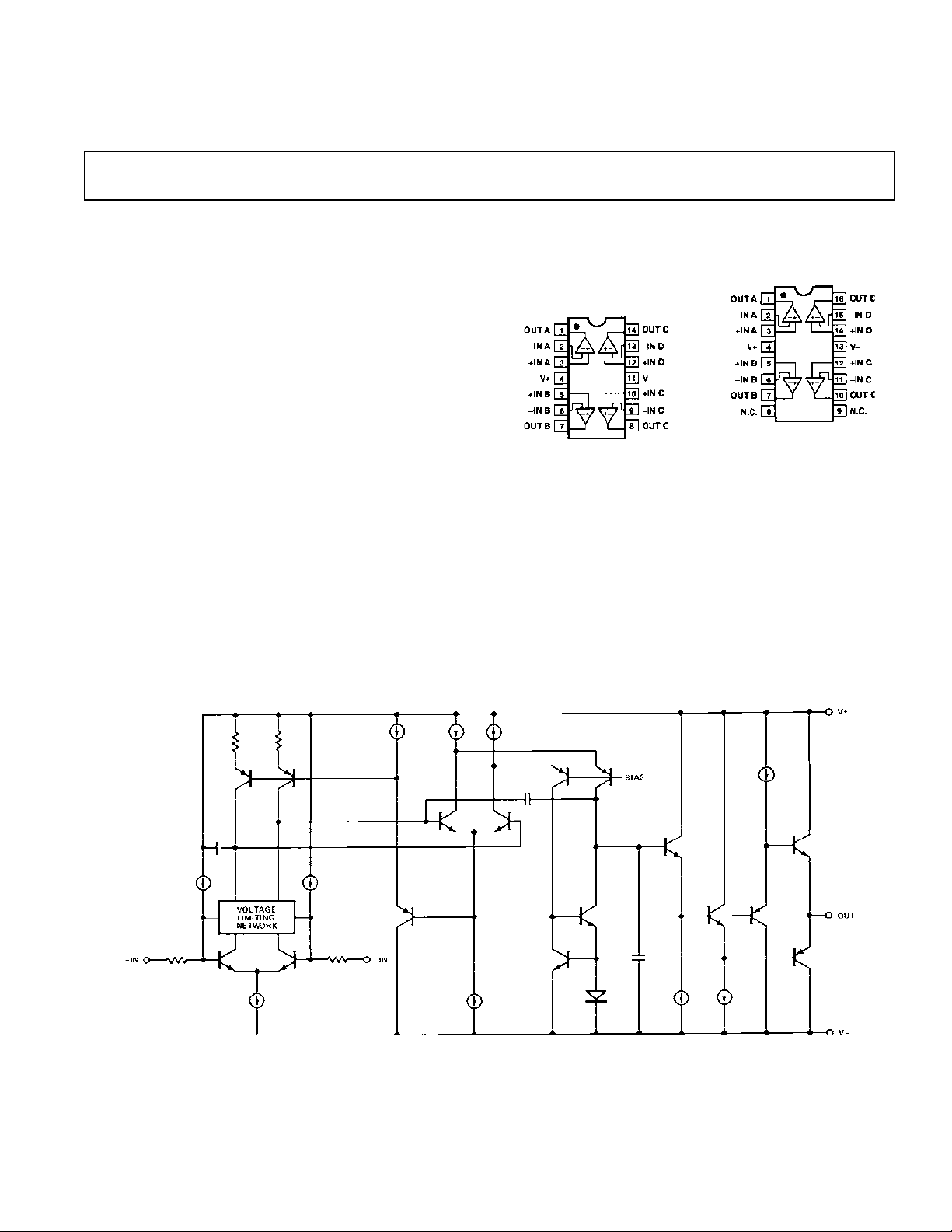
nulling. The OP400 conforms to the industry-standard quad
pinout which does not have null terminals.
Operational Amplifier
OP400
PIN CONNECTIONS
14-PIN HERMETIC DIP
(Y-Suffix)
14-PIN PLASTIC DIP
(P-Suffix)
The OP400 features low power consumption, drawing less than
725 mA per amplifier. The total current drawn by this quad
amplifier is less than that of a single OP07, yet the OP400 offers
significant improvements over this industry standard op amp.
Voltage noise density of the OP400 is a low 11 nV/
which is half that of most competitive devices.
The OP400 is pin-compatible with the LM148, HA4741,
RM4156, and LT1014 operational amplifiers and can be used
to upgrade systems using these devices. The OP400 is an ideal
choice for applications requiring multiple precision operational
amplifiers and where low power consumption is critical.
16-PIN SOL
(S-Suffix)
÷
Hz at 10 Hz,
Figure 1. Simplified Schematic (One of Four Amplifiers is Shown)
REV. A
Information furnished by Analog Devices is believed to be accurate and
reliable. However, no responsibility is assumed by Analog Devices for its
use, nor for any infringements of patents or other rights of third parties that
may result from its use. No license is granted by implication or otherwise
under any patent or patent rights of Analog Devices.
One Technology Way, P.O. Box 9106, Norwood, MA 02062-9106, U.S.A.
Tel: 781/329-4700 www.analog.com
Fax: 781/326-8703 © Analog Devices, Inc., 2002
Page 2

OP400–SPECIFICATIONS
ELECTRICAL CHARACTERISTICS
(@ VS = 15 V, TA = 25ⴗC, unless otherwise noted.)
OP400A/E OP400F OP400G/H
Parameter Symbol Conditions Min Typ Max Min Typ Max Min Typ Max Unit
Input Offset
Voltage V
OS
40 150 60 230 80 300 mV
Long-Term Input
Voltage Stability 0.1 0.1 0.1 mV/mo
Input Offset
Current I
OS
VCM = ∞V 0.1 1.0 0.1 2.0 0.1 3.5 nA
Input Bias
Current I
B
VCM = ∞V0.753.0 0.75 6.0 0.75 7.0 nA
Input Noise
Voltage e
Input Noise
Voltage Density
n p-p
1
e
n
0.1 Hz to 10 Hz 0.5 0.5 0 5 mV p-p
fO = 10 Hz
= 1000 Hz
f
O
1
1
22 36 22 36 22
11 18 11 18 11 nV/÷Hz
Input Noise
Current i
n p-p
0.1 Hz to 10 Hz 15 15 15 pAp-p
Input Noise
Current Density i
n
fO= 10 Hz 0.6 0.6 0.6 pA/÷Hz
Input Resistance
Differential Mode R
IN
10 10 10 MW
Input Resistance
Common Mode R
INCM
200 200 200 GW
Large Signal
Voltage Gain A
Input Voltage
Range
3
VO
R
IVR ±12 ±13 ±12 ±13 ±12 ±13 V
VO = ±10 V
R
= 10 kW 5000 12000 3000 7000 3000 7000
L
= 2 kW 2000 3500 1500 3000 1500 3000 V/mV
L
Common Mode
Rejection CMR VCM = 12 V 120 140 115 140 110 135 dB
Power Supply
Rejection Ratio PSRR V
= 3 V
S
to 18 V 0.1 1.8 0.1 3.2 0.2 5 6 mV/V
Output Voltage
Swing V
O
RL = 10 kW±12 ± 12.6 ±12 ±12.6 ±12 ±12.6 V
R
= 2 kW±11 ± 12.2 ±11 ±12.2 ±11 ±12.2
L
Supply Current
Per Amplifier I
SY
No Load 600 725 600 725 600 725 mA
Slew Rate SR 0.1 0.15 0.1 0.15 0.1 0.15 V/ms
Gain Bandwidth
Product GBWP A
= 1 500 500 500 kHz
V
Channel
Separation CS V
= 20 V p-p 123 135 123 135 123 135 dB
O
= 10 Hz
f
O
2
Input
Capacitance C
IN
3.2 3.2 3.2 pF
Capacitive Load
Stability A
V
= 1
No Oscillations 10 10 10 nF
NOTES
1
Sample tested
2
Guaranteed but not 100% tested.
3
Guaranteed by CMR test
–2–
REV. A
Page 3
OP400
SPECIFICATIONS
ELECTRICAL CHARACTERISTICS
(continued)
(@ VS = 15 V, –55ⴗC
<
T
= 125ⴗC for OP400A, unless otherwise noted.)
A
Parameter Symbol Conditions Min Typ Max Unit
Input Offset Voltage VoS 70 270 mV
Average Input Offset Voltage Drift TCV
Input Offset Current I
Input Bias Current I
Large Signal Voltage Gain A
Input Voltage Range
*
OS
B
VO
IVR ±12 ±12.5 V
OS
VCM = 0 V 01 2.5 nA
VCM = 0 V 1.3 5.0 nA
VO = ±10 V RL = 10 kW 3000 9000 V/mV
R
= 2 kW 1000 2300
L
0.3 12 mV/∞C
Common Mode Rejection CMR VCM = ±12 V 115 130 dB
Power Supply Rejection Ratio PSRR VO = 3 V to 18 V 0.2 3.2 mV/V
Output Voltage Swing VO RL = 10 kW±12 ± 12.4
= 2 kW±11 ±12 V
R
L
Supply Current Per Amplifier I
SY
No Load 600 775 mA
Capacitive Load Stability AV = 1 8 nF
No Oscillations
NOTE
*
Guaranteed by CMR test
(@ VS = ⴞ15 V, –25ⴗC < TA S ⴞ85ⴗC for OP400E/F, 0ⴗC S TA < 70ⴗC for OP400G,
ELECTRICAL CHARACTERISTICS
–40ⴗC < TA < +85ⴗC for OP400H, unless otherwise noted.)
OP400A/E OP400F OP400G/H
Parameter Symbol Conditions Min Typ Max Min Typ Max Min Typ Max Unit
Input Offset
Voltage V
OS
60 220 80 350 110 400 mV
Average Input Offset
Voltage Drift TCV
OS
0 3 1.2 0.3 2.0 0.6 2.5 mV/∞C
Input Offset
Current I
OS
VCM = 0 V
E, F, G Grades 0.1 2.5 0.1 3.5 0.2 6.0
H Grade 0.2 12.0 nA
Input Bias
Current I
B
VCM = 0 V
E, F, G Grades 0.1 2.5 0.1 3.5 1.0 12.0
H Grade 1.0 20.0 nA
Large-Signal
Voltage Gain A
VO
VCM = 0 V
= 10 kW 3000 10000 2000 5000 2000 5000
R
L
RL = 2 kW 1500 2700 1000 2000 1000 2000 V/mv
Input Voltage
Range IVR
*
±12 ±12.5 ±12 ±12.5 ±12 ± 12.5 V
Common-Mode
Rejection CMR VCM = ±12 V 115 135 110 135 105 130 dB
Power Supply
Rejection Ratio PSRR V
= ±3 V
S
to ±18 V 0.15 3.2 0.15 5.6 0.3 10.0 mV/V
Output Voltage
Swing V
O
RL = 10 kW±12 ± 12.4 ±12 ±12.4 ±12 ±12.6 V
RL = 2 kW±11 ± 12 ±11 ± 12 ±11 ± 12.2
Supply Current
Per Amplifier I
SY
No Load 600 775 600 775 600 775 mA
Capacitive Load 10 10 10 nF
Stability No Oscillations
NOTE
*
Guaranteed by CMR test.
–3–REV. A
Page 4
OP400
WARNING!
ESD SENSITIVE DEVICE
ORDERING INFORMATION
TA = 25ⴗC Package Operating
V
Max CerDIP Temperature
OS
(mV) 14-Lead Plastic Range
150 OP400AY MIL
150 OP400EY IND
230 OP400FY IND
300 OP400GP COM
300 OP400GS COM
300 OP400HP XIND
300 OP400HS XIND
NOTES
1
For devices processed in total compliance to MIL-STD-883, add/883after part
number. Consult factory for 883 data sheet.
2
Burn-in is available on commercial and industrial temperature range parts in
CerDIP, plastic DIP, and TO-can packages.
For Military processed devices, please refer to the standard
microcircuit drawing (SMD) available at
www.dscc.dla.mil/programs/milspec/default.asp
SMD Part Number ADI Equivalent
5962-8777101M3A OP400ATCMDA
5962-8777101MCA OP400AYMDA
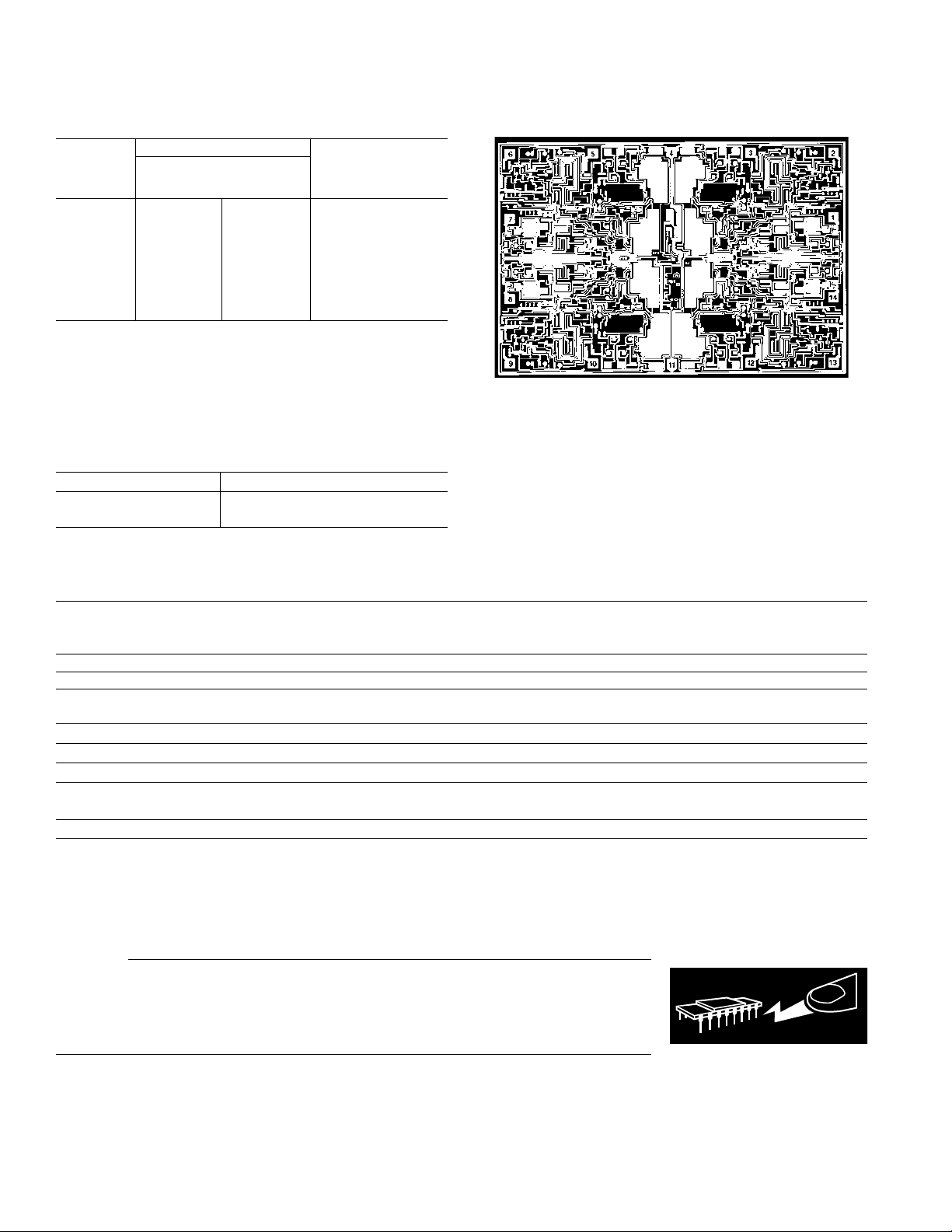
DICE CHARACTERISTICS
DIE SIZE 0.181 ⴛ 0.123 inch, 22,263 sq. milts
(4.60 ⴛ 3.12 mm, 14.35 sq. mm)
1. OUT A 8. OUT C
2. –IN A 9. –IN C
3. +INA 10. +IN C
4. V+ 11. V-
5. +IN B 12. +IND
6. –IN B 13. –IN D
7. OUT B 14. OUT D
WAFER TEST LIMITS
(@ VS = ⴞ15 V, TA = 25ⴗC, unless otherwise noted.)
OP400GBC
Parameter Symbol Conditions Limit Unit
Input Offset Voltage V
Input Offset Current V
Input Bias Current I
Large Signal A
OS
OS
B
VO
VCM = 0 V 2 nA Max
VCM = 0 V 6 nA Max
VO = ±10 V RL = 10 kW 3000
230 mA Max
Voltage Gain Rig 2 kW 1500 V/mV Min
Input Voltage Range
*
IVR
*
±12 V Min
Common Mode Rejection CMR VCM = ±12 V 115 dB Min
Power Supply Rejection Ratio PSRR VS = ±3 V to ±18 V 3.2 mV/V Max
Output Voltage Swing V
Supply Current Per Amplifier I
NOTE
*
Guaranteed by CMR test.
Electrical tests are performed at wafer probe to the limits shown Due to variations in assembly methods and normal yield loss, yield after packaging is not guaranteed
for standard product dice. Consult factory to negotiate specifications based on dice lot qualification through sample lot assembly and testing.
O
SY
RL = 10 kW
R
= 2 kW±12 V Min
L
No Load 725 mA Max
CAUTION
ESD (electrostatic discharge) sensitive device. Electrostatic charges as high as 4000 V readily
accumulate on the human body and test equipment and can discharge without detection. Although the
OP400 features proprietary ESD protection circuitry, permanent damage may occur on devices
subjected to high-energy electrostatic discharges. Therefore, proper ESD precautions are recommended
to avoid performance degradation or loss of functionality.
–4–
REV. A
Page 5

Typical Performance Characteristics–OP400
TPC 1. Warm-Up Drift
TPC 4. Input Offset Current
vs. Temperature
TPC 2. Input Offset Voltage
vs. Temperature
TPC 5. Input Bias Current vs.
Common-Mode Voltage
TPC 3. Input Bias Current
vs. Temperature
TPC 6. Common-Mode Rejection
vs. Frequency
TPC 7. Noise Voltage Density
vs. Frequency
TPC 8. Current Noise Density
vs. Frequency
–5–REV. A
TPC 9. 0.1 Hz to10 Hz Noise
Page 6

OP400
TPC 10. Total Supply Current
vs. Supply Voltage
TPC 13. Power Supply
Rejection vs. Temperature
TPC 11. Total Supply Current
vs. Temperature
TPC 14. Open-Loop Gain vs.
Temperature
TPC 12. Power Supply Rejection
vs. Frequency
TPC 15. Open-Loop Gain and
Phase Shift vs. Frequency
TPC 16. Closed-Loop Gain
vs. Frequency
TPC 17. Maximum Output
Swing Frequency
–6–
TPC 18. Total Harmonic
Distortion vs. Frequency
REV. A
Page 7

OP400
TPC 19. Overshoot vs.
Capacitive Load
TPC 22. Large-Signal
Transient Response
TPC 20. Short Circuit vs. Time
TPC 23. Small-Signal
Transient Response
TPC 21. Channel Separation
vs. Frequency
TPC 24. Small-Signal Transient
Response C
LOAD
= 1nF
Figure 2. Noise Test Schematic
–7–REV. A
Page 8

OP400
Figure 3. Burn-In Circuit
APPLICATIONS INFORMATION
The OP400 is inherently stable at all gains and is capable of
driving large capacitive loads without oscillating. Nonetheless,
good supply decoupling is highly recommended. Proper supply
decoupling reduces problems caused by supply line noise and
improves the capacitive load driving capability of the OP400.
Total supply current can be reduced by connecting the inputs of
an unused amplifier to –V. This turns the amplifier off, lowering
the total supply current.
Table I. Gain Bandwidth
Gain Bandwidth
5 150 kHz
10 67 kHz
100 7.5 kHz
1000 500 Hz
The output signal is specified with respect to the reference
input, which is normally connected to analog ground. The reference input can be used to offset the output from –10 V to +10 V
if required.
APPLICATIONS
Dual Low-Power Instrumentation Amplifier
A dual instrumentation amplifier that consumes less than 33 mW
of power per channel is shown in Figure 1. The linearity of the
instrumentation amplifier exceeds 16 bits in gains of 5 to 200
and is better than 14 bits in gains from 200 to 1000. CMRR is
above 115 dB (G = 1000). Offset voltage drift is typically 0.4
mV/∞C over the military temperature range which is comparable
to the best monolithic instrumentation amplifiers. The bandwidth of the low-power instrumentation amplifier is a function
of gain and is shown in Table I.
Figure 4. Dual Low-Power Instrumentation Amplifier
–8–
REV. A
Page 9

Figure 5. Bipolar Current Transmitter
BIPOLAR CURRENT TRANSMITTER
In the circuit of Figure 5, which is an extension of the standard
three op amp instrumentation amplifier, the output current is
proportional to the differential input voltage. Maximum output
current is ±5 mA with voltage compliance equal to ±10 V when
using ±15 V supplies. Output impedance of the current transmitter exceeds 3 MW and linearity is better than 16 bits with gain
set for a full scale input of ±100 mV.
OP400
DIFFERENTIAL OUTPUT INSTRUMENTATION AMPLIFIER
The output voltage swing of a single-ended instrumentation
amplifier is limited by the supplies, normally at ±15 V, to a
maximum of 24 V p-p. The differential output instrumentation
amplifier of Figure 6 can provide an output voltage swing of
48 V p-p when operated with ±15 V supplies. The extended
output swing is due to the opposite polarity of the outputs. Both
outputs will swing 24 V p-p but with opposite polarity, for a
total output voltage swing of 48 V p-p. The reference input can
be used to set a common-mode output voltage over the range
±10 V. PSRR of the amplifier is less than 1 mV/V with CMRR
(G = 1000) better than 115 dB. Offset voltage drift is typically
0.4 mV/∞C over the military temperature range.
Figure 6. Differential Output Instrumentation Amplifier
–9–REV. A
Page 10

OP400
MULTIPLE OUTPUT TRACKING VOLTAGE
REFERENCE
Figure 7 shows a circuit that provides outputs of 10 V, 7.5 V, 5 V,
and 2.5 V for use as a system voltage reference. Maximum
output current from each reference is 5 mA with load regulation
under 25 mV/mA. Line regulation is better than 15 mV/V and
output voltage drift is under 20 mV/∞C. Output voltage noise
from 0.1 Hz to 10 Hz is typically 75 mV p-p from the 10 V output
and proportionately less from the 7.5 V, 5 V, and 2.5 V outputs.
Figure 7. Multiple-Output Tracking Voltage Reference
–10–
REV. A
Page 11

OUTLINE DIMENSIONS
14
1
7
8
PIN 1
0.795 (20.19)
0.725 (18.42)
0.280 (7.11)
0.240 (6.10)
0.100 (2.54)
BSC
SEATING
PLANE
0.060 (1.52)
0.015 (0.38)
0.210 (5.33)
MAX
0.022 (0.558)
0.014 (0.356)
0.160 (4.06)
0.115 (2.93)
0.070 (1.77)
0.045 (1.15)
0.130
(3.30)
MIN
0.195 (4.95)
0.115 (2.93)
0.015 (0.381)
0.008 (0.204)
0.325 (8.25)
0.300 (7.62)
Dimensions shown in inches and (mm).
OP400
14-Lead Hermetic DIP Package
(Y-Suffix)
0.005 (0.13) MIN 0.098 (2.49) MAX
PIN 1
0.200
(5.08)
MAX
0.200 (5.08)
0.125 (3.18)
14
17
0.100 (2.54)
0.785 (19.94) MAX
0.023 (0.58)
0.014 (0.36)
BSC
0.070 (1.78)
0.030 (0.76)
8
0.310 (7.87)
0.220 (5.59)
0.060 (1.52)
0.015 (0.38)
0.150
(3.81)
MIN
SEATING
PLANE
0.320 (8.13)
0.290 (7.37)
15
0
0.4133 (10.50)
0.3977 (10.00)
16
1
0.015 (0.38)
0.008 (0.20)
16-Lead SOL Package
(S-Suffix)
9
0.2992 (7.60)
0.2914 (7.40)
8
14-Lead Plastic DIP Package
(P-Suffix)
0.4193 (10.65)
0.3937 (10.00)
PIN 1
0.0118 (0.30)
0.0040 (0.10)
0.050 (1.27)
BSC
0.1043 (2.65)
0.0926 (2.35)
0.0192 (0.49)
0.0138 (0.35)
SEATING
PLANE
0.0125 (0.32)
0.0091 (0.23)
0.0291 (0.74)
0.0098 (0.25)
8ⴗ
0ⴗ
ⴛ 45ⴗ
0.0500 (1.27)
0.0157 (0.40)
Revision History
Location Page
Data Sheet changed from REV. 0 to REV. A.
Edits to FEATURES . . . . . . . . . . . . . . . . . . . . . . . . . . . . . . . . . . . . . . . . . . . . . . . . . . . . . . . . . . . . . . . . . . . . . . . . . . . . . . . . . . . . . 1
Edits to ORDERING INFORMATION . . . . . . . . . . . . . . . . . . . . . . . . . . . . . . . . . . . . . . . . . . . . . . . . . . . . . . . . . . . . . . . . . . . . . . 1
Edits to PIN CONNECTIONS . . . . . . . . . . . . . . . . . . . . . . . . . . . . . . . . . . . . . . . . . . . . . . . . . . . . . . . . . . . . . . . . . . . . . . . . . . . . . 1
Edits to GENERAL DESCRIPTIONS . . . . . . . . . . . . . . . . . . . . . . . . . . . . . . . . . . . . . . . . . . . . . . . . . . . . . . . . . . . . . . . . . . . . . 1, 2
Edits to PACKAGE TYPE . . . . . . . . . . . . . . . . . . . . . . . . . . . . . . . . . . . . . . . . . . . . . . . . . . . . . . . . . . . . . . . . . . . . . . . . . . . . . . . . 2
–11–REV. A
Page 12

C00304–0–4/02(A)
–12–
PRINTED IN U.S.A.
 Loading...