

Page 1
Precision Rail-to-Rail
A
T
2
O
www.BDTIC.com/ADI
Input and Output Operational Amplifiers
FEATURES
Single-supply operation
Wide bandwidth: 4 MHz
Low offset voltage: 65 μV
Unity-gain stable
High slew rate: 4.0 V/μs
Low noise: 3.9 nV/√Hz
APPLICATIONS
Battery-powered instrumentation
Power supply control and protection
Telecommunications
DAC output amplifier
ADC input buffer
GENERAL DESCRIPTION
The OP184/OP284/OP484 are single, dual, and quad single-supply,
4 MHz bandwidth amplifiers featuring rail-to-rail inputs and
outputs. They are guaranteed to operate from 3 V to 36 V (or
±1.5 V to ±18 V).
These amplifiers are superb for single-supply applications requiring
both ac and precision dc performance. The combination of wide
bandwidth, low noise, and precision makes the OP184/OP284/
OP484 useful in a wide variety of applications, including filters
and instrumentation.
Other applications for these amplifiers include portable telecommunications equipment, power supply control and protection,
and use as amplifiers or buffers for transducers with wide output
ranges. Sensors requiring a rail-to-rail input amplifier include
Hall effect, piezoelectric, and resistive transducers.
The ability to swing rail-to-rail at both the input and output
enables designers to build multistage filters in single-supply
systems and to maintain high signal-to-noise ratios.
The OP184/OP284/OP484 are specified over the hot extended
industrial temperature range of −40°C to +125°C. The single
OP184 is available in 8-lead SOIC surface mount packages. The
dual OP284 is available in 8-lead PDIP and SOIC surface mount
packages. The quad OP484 is available in 14-lead PDIP and
14-lead, narrow-body SOIC packages.
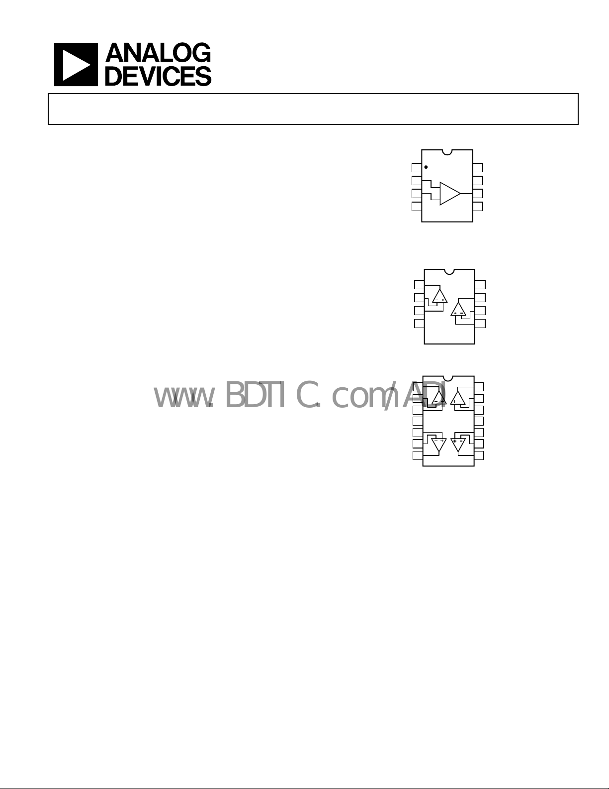
OP184/OP284/OP484
PIN CONFIGURATIONS
OP184
1
DNC
–IN A
2
–
3
+IN
V–
NOTES
1. NC = NO CONNEC
. DNC = DO NOT CO NNECT
4
(Not to Scale)
+
TOP VIEW
Figure 1. 8-Lead SOIC (S-Suffix)
OP284
1
UT A
2
–IN A
3
+IN A
4
V–
TOP VIEW
(Not to Scale)
Figure 2. 8-Lead PDIP (P-Suffix)
8-Lead SOIC (S-Suffix)
1
OUT A
2
–IN A
3
+IN A
V+
+IN B
–IN B
OUT B
4
TOP VIEW
(Not to Scale)
5
6
7
OP484
Figure 3. 14-Lead PDIP (P-Suffix)
14-Lead Narrow-Body SOIC (S-Suffix)
8
7
6
5
14
13
12
11
10
8
7
6
5
9
8
NC
V+
OUT A
DNC
V+
OUT B
–IN B
+IN B
OUT D
–IN D
+IN D
V–
+IN C
–IN C
OUT C
00293-001
00293-002
00293-003
Rev. F
Information furnished by Analog Devices is believed to be accurate and reliable. However, no
responsibility is assumed by Analog Devices for its use, nor for any infringements of patents or other
rights of third parties that may result from its use. Specifications subject to change without notice. No
license is granted by implication or otherwise under any patent or patent rights of Analog Devices.
Trademarks and registered trademarks are the property of their respective owners.
One Technology Way, P.O. Box 9106, Norwood, MA 02062-9106, U.S.A.
Tel: 781.329.4700 www.analog.com
Fax: 781.461.3113 ©1996–2008 Analog Devices, Inc. All rights reserved.
Page 2

OP184/OP284/OP484
www.BDTIC.com/ADI
TABLE OF CONTENTS
Features .............................................................................................. 1
Applications ....................................................................................... 1
General Description ......................................................................... 1
Pin Configurations ........................................................................... 1
Revision History ............................................................................... 2
Specifications ..................................................................................... 3
Electrical Characteristics ............................................................. 3
Absolute Maximum Ratings ............................................................ 6
Thermal Resistance ...................................................................... 6
ESD Caution .................................................................................. 6
Typical Performance Characteristics ............................................. 7
Applications Information .............................................................. 14
Functional Description .............................................................. 14
Input Overvoltage Protection ................................................... 14
REVISION HISTORY
9/08—Rev. E to Rev. F
Changes to General Description .................................................... 1
Changes to Figure 4 .......................................................................... 6
Changes to Low Dropout Regulator with Current Limiting .... 20
7/08—Rev. D to Rev. E
Changes to Figure 1 .......................................................................... 1
Changes to Figure 12 ........................................................................ 8
Changes to Figure 36 and Figure 37 ............................................. 12
Changes to Designing Low Noise Circuits in Single-Supply
Applications Section ....................................................................... 15
Updated Outline Dimensions ....................................................... 21
Changes to Ordering Guide .......................................................... 22
4/06—Rev. C to Rev. D
Changes to Table 1 ............................................................................ 3
Changes to Table 2 ............................................................................ 4
Changes to Table 3 ............................................................................ 5
Deleted Reference to 1993 System Applications Guide............... 15
Output Phase Reversal ............................................................... 15
Designing Low Noise Circuits in Single-Supply
Applications ................................................................................ 15
Overdrive Recovery ................................................................... 16
Single-Supply, 3 V Instrumentation Amplifier ...................... 16
2.5 V Reference from a 3 V Supply .......................................... 17
5 V Only, 12-Bit DAC Swings Rail-to-Rail ............................. 17
High-Side Current Monitor ...................................................... 18
Capacitive Load Drive Capability ............................................ 18
Low Dropout Regulator with Current Limiting ..................... 18
3 V, 50 Hz/60 Hz Active Notch Filter with False Ground ..... 20
Outline Dimensions ....................................................................... 21
Ordering Guide .......................................................................... 22
3/06—Rev. B to Rev. C
Changes to Figure 1 Caption........................................................... 1
Changes to Table 1 ............................................................................ 3
Changes to Table 2 ............................................................................ 4
Changes to Table 3 ............................................................................ 5
Changes to Table 4 ............................................................................ 6
Changes to Figure 5 through Figure 9 ........................................... 7
Changes to Functional Description Section ............................... 14
Deleted SPICE Macro Model ........................................................ 21
Updated Outline Dimensions ....................................................... 21
Changes to Ordering Guide .......................................................... 22
9/02—Rev. A to Rev. B
Changes to Pin Configurations ...................................................... 1
Changes to Specifications, Input Bias Current Maximum.......... 2
Changes to Ordering Guide ............................................................ 5
Updated Outline Dimensions ....................................................... 19
6/02—Rev. 0 to Rev. A
10/96—Revision 0: Initial Version
Rev. F | Page 2 of 24
Page 3
OP184/OP284/OP484
www.BDTIC.com/ADI
SPECIFICATIONS
ELECTRICAL CHARACTERISTICS
VS = 5.0 V, VCM = 2.5 V, TA = 25°C, unless otherwise noted.
Table 1.
Parameter Symbol Conditions Min Typ Max Unit
INPUT CHARACTERISTICS
Offset Voltage, OP184/OP284E Grade1VOS 65 V
−40°C ≤ TA ≤ +125°C 165 V
Offset Voltage, OP184/OP284F Grade
−40°C ≤ TA ≤ +125°C 350 V
Offset Voltage, OP484E Grade
–40°C ≤ TA ≤ +125°C 175 V
Offset Voltage, OP484F Grade
–40°C ≤ TA ≤ +125°C 450 V
Input Bias Current IB 60 450 nA
–40°C ≤ TA ≤ +125°C 600 nA
Input Offset Current IOS 2 50 nA
–40°C ≤ TA ≤ +125°C 50 nA
Input Voltage Range 0 5 V
Common-Mode Rejection Ratio CMRR VCM = 0 V to 5 V 60 dB
V
Large Signal Voltage Gain AVO RL = 2 kΩ, 1 V ≤ VO ≤ 4 V 50 240 V/mV
R
Bias Current Drift ∆IB/∆T 150 pA/°C
OUTPUT CHARACTERISTICS
Output Voltage High VOH IL = 1.0 mA 4.85 V
Output Voltage Low VOL IL = 1.0 mA 125 mV
Output Current I
POWER SUPPLY
Power Supply Rejection Ratio PSRR VS = 2.0 V to 10 V, −40°C ≤ TA ≤ +125°C 76 dB
Supply Current/Amplifier ISY VO = 2.5 V, −40°C ≤ TA ≤ +125°C 1.45 mA
Supply Voltage Range VS 3 36 V
DYNAMIC PERFORMANCE
Slew Rate SR RL = 2 kΩ 1.65 2.4 V/µs
Settling Time tS To 0.01%, 1.0 V step 2.5 µs
Gain Bandwidth Product GBP 3.25 MHz
Phase Margin ΦM 45 Degrees
NOISE PERFORMANCE
Voltage Noise en p-p 0.1 Hz to 10 Hz 0.3 V p-p
Voltage Noise Density en f = 1 kHz 3.9 nV/√Hz
Current Noise Density in 0.4 pA/√Hz
1
Input offset voltage measurements are performed by automated test equipment approximately 0.5 seconds after application of power.
1
V
1
V
1
V
125 V
OS
75 V
OS
150 V
OS
= 1.0 V to 4.0 V, −40°C ≤ TA ≤ +125°C 86 dB
CM
= 2 kΩ, −40°C ≤ TA ≤ +125°C 25 V/mV
L
±6.5 mA
OUT
Rev. F | Page 3 of 24
Page 4
OP184/OP284/OP484
www.BDTIC.com/ADI
VS = 3.0 V, VCM = 1.5 V, TA = 25°C, unless otherwise noted.
Table 2.
Parameter Symbol Conditions Min Typ Max Unit
INPUT CHARACTERISTICS
Offset Voltage, OP184/OP284E Grade
−40°C ≤ TA ≤ +125°C 165 V
Offset Voltage, OP184/OP284F Grade
−40°C ≤ TA ≤ +125°C 350 V
Offset Voltage, OP484E Grade
–40°C ≤ TA ≤ +125°C 200 V
Offset Voltage, OP484F Grade
–40°C ≤ TA ≤ +125°C 450 V
Input Bias Current IB 60 450 nA
−40°C ≤ TA ≤ +125°C 600 nA
Input Offset Current IOS −40°C ≤ TA ≤ +125°C 50 nA
Input Voltage Range 0 3 V
Common-Mode Rejection Ratio CMRR VCM = 0 V to 3 V 60 dB
V
OUTPUT CHARACTERISTICS
Output Voltage High VOH IL = 1.0 mA 2.85 V
Output Voltage Low VOL IL = 1.0 mA 125 mV
POWER SUPPLY
Power Supply Rejection Ratio PSRR VS = ±1.25 V to ±1.75 V 76 dB
Supply Current/Amplifier ISY VO = 1.5 V, −40°C ≤ TA ≤ +125°C 1.35 mA
DYNAMIC PERFORMANCE
Gain Bandwidth Product GBP 3 MHz
NOISE PERFORMANCE
Voltage Noise Density en f = 1 kHz 3.9 nV/√Hz
1
Input offset voltage measurements are performed by automated test equipment approximately 0.5 seconds after application of power.
1
V
1
V
1
V
1
V
65 V
OS
125 V
OS
100 V
OS
150 V
OS
= 0 V to 3 V, −40°C ≤ TA ≤ +125°C 56 dB
CM
Rev. F | Page 4 of 24
Page 5
OP184/OP284/OP484
www.BDTIC.com/ADI
VS = ±15.0 V, VCM = 0 V, TA = 25°C, unless otherwise noted.
Table 3.
Parameter Symbol Conditions Min Typ Max Unit
INPUT CHARACTERISTICS
Offset Voltage, OP184/OP284E Grade1VOS 100 V
−40°C ≤ TA ≤ +125°C 200 V
Offset Voltage, OP184/OP284F Grade
−40°C ≤ TA ≤ +125°C 375 V
Offset Voltage, OP484E Grade
−40°C ≤ TA ≤ +125°C 300 V
Offset Voltage, OP484F Grade
−40°C ≤ TA ≤ +125°C 500 V
Input Bias Current IB 80 450 nA
−40°C ≤ TA ≤ +125°C 575 nA
Input Offset Current IOS −40°C ≤ TA ≤ +125°C 50 nA
Input Voltage Range −15 +15 V
Common-Mode Rejection Ratio CMRR VCM = −14.0 V to +14.0 V, −40°C ≤ TA ≤ +125°C 86 90 dB
V
Large Signal Voltage Gain AVO R
R
Offset Voltage Drift E Grade ∆VOS/∆T 0.2 2.00 V/°C
Bias Current Drift ∆VB/∆T 150 pA/°C
OUTPUT CHARACTERISTICS
Output Voltage High VOH IL = 1.0 mA 14.8 V
Output Voltage Low VOL IL = 1.0 mA −14.875 V
Output Current I
POWER SUPPLY
Power Supply Rejection Ratio PSRR VS = ±2.0 V to ±18 V, −40°C ≤ TA ≤ +125°C 90 dB
Supply Current/Amplifier ISY VO = 0 V, −40°C ≤ TA ≤ +125°C 2.0 mA
Supply Current/Amplifier ISY V
DYNAMIC PERFORMANCE
Slew Rate SR RL = 2 kΩ 2.4 4.0 V/µs
Full-Power Bandwidth BWp 1% distortion, RL = 2 kΩ, VO = 29 V p-p 35 kHz
Settling Time tS To 0.01%, 10 V step 4 µs
Gain Bandwidth Product GBP 4.25 MHz
Phase Margin ΦM 50 Degrees
NOISE PERFORMANCE
Voltage Noise en p-p 0.1 Hz to 10 Hz 0.3 µV p-p
Voltage Noise Density en f = 1 kHz 3.9 nV/√Hz
Current Noise Density in 0.4 pA/√Hz
1
Input offset voltage measurements are performed by automated test equipment approximately 0.5 seconds after application of power.
1
V
1
V
1
V
175 V
OS
150 V
OS
250 V
OS
= −15.0 V to +15.0 V 80 dB
CM
= 2 kΩ, −10 V ≤ VO ≤ 10 V 150 1000 V/mV
L
= 2 kΩ, −40 V ≤ TA ≤ +125°C 75 V/mV
L
±10 mA
OUT
= ±18 V, −40°C ≤ TA ≤ +125°C 2.25 mA
S
Rev. F | Page 5 of 24
Page 6
OP184/OP284/OP484
V
www.BDTIC.com/ADI
ABSOLUTE MAXIMUM RATINGS
Table 4.
Parameter Rating
Supply Voltage ±18 V
Input Voltage ±18 V
Differential Input Voltage1 ±0.6 V
Output Short-Circuit Duration to GND Indefinite
Storage Temperature Range
P-Suffix, S-Suffix Packages −65°C to +150°C
Operating Temperature Range
OP184/OP284/OP484E/OP484F −40°C to +125°C
Junction Temperature Range
P-Suffix, S-Suffix Packages −65°C to +150°C
Lead Temperature
(Soldering 60 sec)
1
For input voltages greater than 0.6 V, the input current should be limited to
less than 5 mA to prevent degradation or destruction of the input devices.
300°C
THERMAL RESISTANCE
θJA is specified for the worst-case conditions; that is, θJA is specified
for a device in socket for PDIP. θ
in the circuit board for SOIC packages.
Table 5. Thermal Resistance
Package Type θJA θ
8-Lead PDIP (P-Suffix) 103 43 °C/W
8-Lead SOIC (S-Suffix) 158 43 °C/W
14-Lead PDIP (P-Suffix) 83 39 °C/W
14-Lead SOIC (S-Suffix) 92 27 °C/W
ESD CAUTION
Stresses above those listed under Absolute Maximum Ratings
may cause permanent damage to the device. This is a stress
rating only; functional operation of the device at these or any
other conditions above those indicated in the operational
section of this specification is not implied. Exposure to absolute
maximum rating conditions for extended periods may affect
device reliability.
Absolute maximum ratings apply to both DICE and packaged
parts, unless otherwise noted.
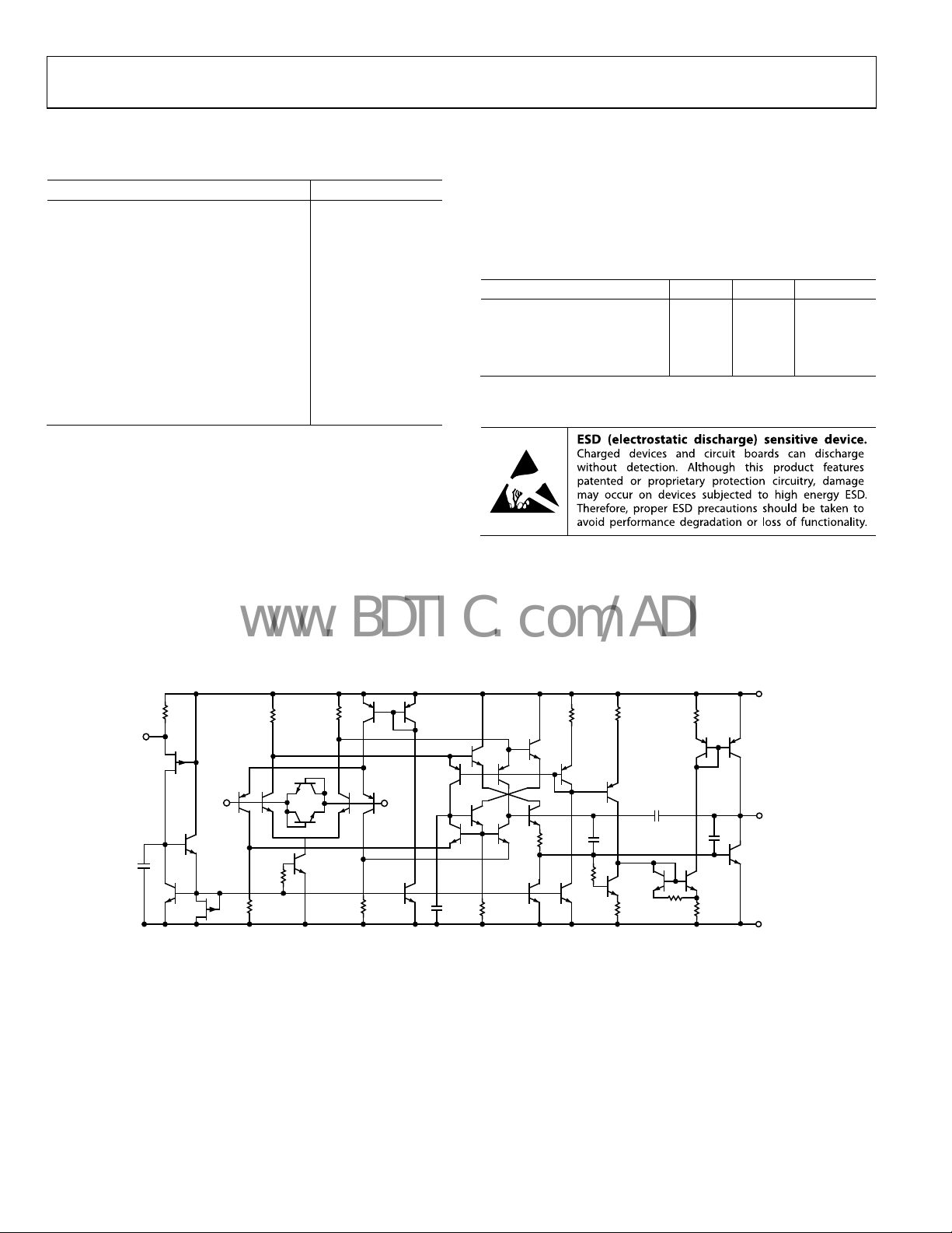
RB1
TP
JB1
–IN +IN
QB2
N+CB1
P+M
QB1
JB2
Q1
R3
Q3
RB2
R1
QL1
QB3
QL2
R4
QB6
Q4
QB5
Q11
Q2
QB4
R2
Q7
Q9
Q5
CC1
Figure 4. Simplified Schematic
Q12
Q8
Q10
Q6
QB7
R5
is specified for a device soldered
JA
Unit
JC
CC
RB3
QB9
R6
R7
QB8
RB4
QB10
CC2
FFC
Q14
Q13
R8
R11
Q15
C
R10
Q17
Q18
OUT
V
EE
00293-004
O
Q16
R9
Rev. F | Page 6 of 24
Page 7
OP184/OP284/OP484
–
www.BDTIC.com/ADI
TYPICAL PERFORMANCE CHARACTERISTICS
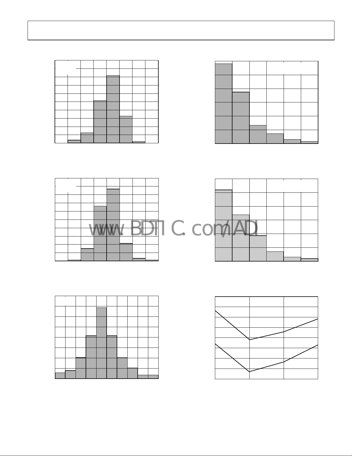
300
VS= 3V
T
= 25°C
A
270
V
= 1.5V
CM
240
210
180
150
QUANTITY
120
90
60
30
0
–100 –75 –50 –25 0 25 50 75 100
INPUT OFFSET VOLTAGE (µV )
Figure 5. Input Offset Voltage Distribution
00293-005
300
250
200
150
QUANTITY
100
50
0
0 0.250.500.751.001.251.
OFFSET VO LTAGE DRIFT , TCVOS (µV/°C)
VS = 5V
–40°C ≤ T
≤ +125°C
A
Figure 8. Input Offset Voltage Drift Distribution
00293-008
50
300
VS= 5V
= 25°C
T
A
270
V
= 2.5V
CM
240
210
180
150
QUANTITY
120
90
60
30
0
–100 –75 –50 –25 0 25 50 75 100
INPUT OFFSET VOLTAGE (µV)
Figure 6. Input Offset Voltage Distribution
200
VS= ±15V
T
= 25°C
A
175
150
125
100
QUANTITY
75
300
250
200
150
QUANTITY
100
50
00293-006
0
0 0.250.500.751.001.251.
OFFSET VO LTAGE DRIFT , TCVOS (µV/°C)
VS = ±15V
–40°C ≤ T
≤ +125°C
A
00293-009
50
Figure 9. Input Offset Voltage Drift Distribution
–45
–50
–55
–60
–65
40
= +5V
V
S
= VS/2
V
CM
50
25
0
–125 –100 –75 –50 –25 0 25 10050 75 125
INPUT OFFSET VOLTAGE (µV)
00293-007
Figure 7. Input Offset Voltage Distribution
Rev. F | Page 7 of 24
–70
INPUT BIAS CURRENT (nA)
–75
–80
–40 25 85 125
V
= ±15V
S
TEMPERATURE (°C)
Figure 10. Bias Current vs. Temperature
00293-010
Page 8
OP184/OP284/OP484
www.BDTIC.com/ADI
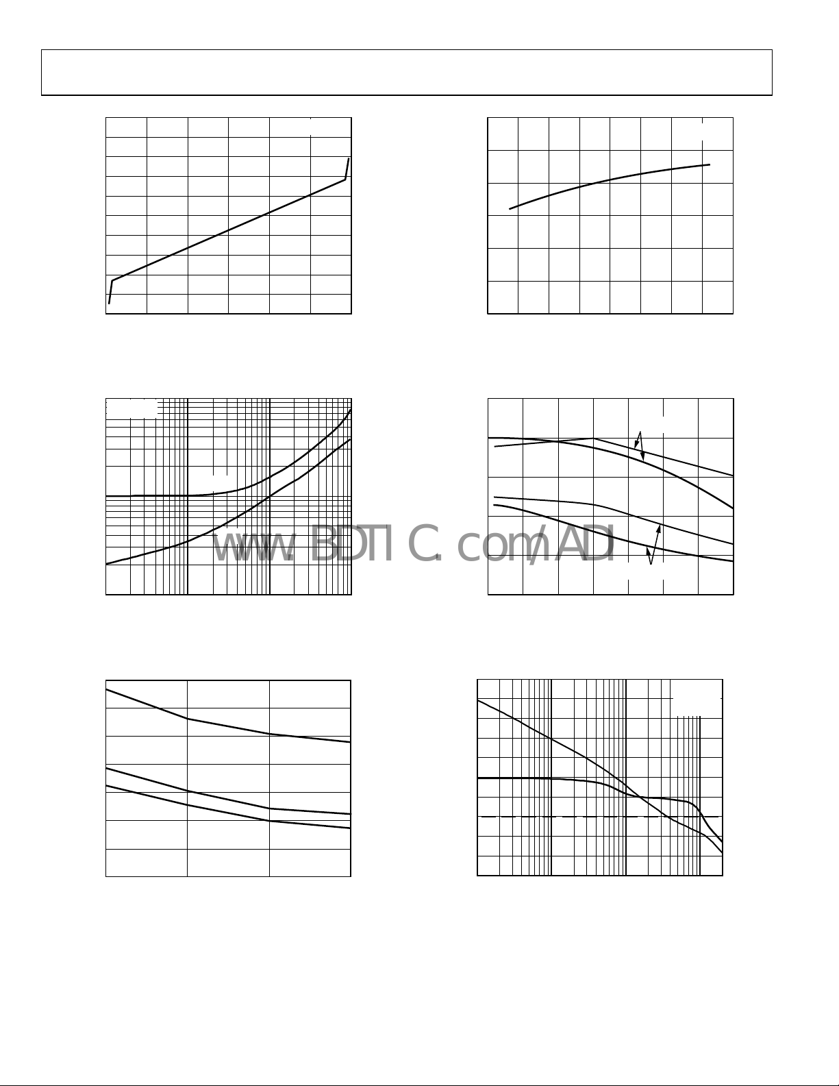
500
400
300
200
100
0
–100
–200
INPUT BIAS CURRENT (nA)
–300
–400
–500
–15 –10 –5 0 5 10 15
COMMON-MODE VOLTAGE (V)
Figure 11. Input Bias Current vs. Common-Mode Voltage
VS = ±15V
00293-011
1.50
1.25
1.00
0.75
0.50
0.25
SUPPLY CURRENT/ PER AMPLIF IER (mA)
0
0 ±2. 5 ±5. 0 ±7. 5 ±10.0 ±12.5 ±15.0 ±17.5 ±20.0
SUPPLY VOLTAGE (V)
Figure 14. Supply Current vs. Supply Voltage
TA = 25°C
00293-014
1000
VS = ±15V
100
OUTPUT VOLTAGE (mV)
10
0.01 0.1 1 10
SOURCE
SINK
LOAD CURRENT (mA)
Figure 12. Output Voltage to Supply Rail vs. Load Current
1.2
1.1
1.0
0.9
0.8
0.7
SUPPLY CURRENT/ AMPLIFIER (mA)
0.6
0.5
–40 25 85 125
TEMPERATURE (°C)
VS = ±15V
V
= +5V
S
= +3V
V
S
Figure 13. Supply Current vs. Temperature
50
40
30
–I
SC
20
+I
SC
10
SHORT-CIRCUIT CURRENT (mA)
00293-012
0
–50 –25 0 25 50 75 100 125
TEMPERATURE (°C)
VS = ±15V
+I
SC
–I
SC
VS = +5V, VCM = +2.5V
00293-015
Figure 15. Short-Circuit Current vs. Temperature
70
60
50
40
30
20
10
0
OPEN-LOOP GAIN (dB)
–10
–20
00293-013
–30
10k 100k 1M 10M
FREQUENCY (Hz)
VS = 5V
T
= 25°C
A
NO LOAD
0
45
90
135
180
225
270
PHASE SHIFT (Degrees)
00293-016
Figure 16. Open-Loop Gain and Phase vs. Frequency (No Load)
Rev. F | Page 8 of 24
Page 9

OP184/OP284/OP484
www.BDTIC.com/ADI
70
60
50
40
30
20
10
0
OPEN-LOOP GAIN (dB)
–10
–20
–30
10k 100k 1M 10M
FREQUENCY (Hz)
VS = 3V
T
= 25°C
A
NO LOAD
Figure 17. Open-Loop Gain and Phase vs. Frequency (No Load)
0
45
90
135
180
225
270
PHASE SHIFT (Degrees)
00293-017
60
50
40
30
20
10
0
–10
CLOSED-LOOP GAIN (dB)
–20
–30
–40
10 1k 100k 10M100 10k 1M
FREQUENCY (Hz)
Figure 20. Closed-Loop Gain vs. Frequency (2 kΩ Load)
VS = 5V
R
= 2kΩ
L
T
= 25°C
A
00293-020
70
60
50
40
30
20
10
0
OPEN-LOOP GAIN (dB)
–10
–20
–30
10k 100k 1M 10M
FREQUENCY (Hz)
VS = ±15V
T
= 25°C
A
NO LOAD
Figure 18. Open-Loop Gain and Phase vs. Frequency (No Load)
2500
2000
1500
1000
OPEN-LOOP GAIN (V/mV)
500
0
–50 1251007550250–25
V
= +5V
S
+1V < V
R
= 2kΩ
L
O
VS = ±15V
–10V < V
R
= 2kΩ
L
< +10V
TEMPERATURE (°C)
< +10V
O
Figure 19. Open-Loop Gain vs. Temperature
0
45
90
135
180
225
270
60
50
40
30
20
10
0
PHASE SHIFT (Degrees)
00293-018
–10
CLOSED-LOOP GAIN (dB)
–20
–30
–40
10 1k 100k 10M100 10k 1M
FREQUENCY (Hz)
VS = ±15V
R
= 2kΩ
L
T
= 25°C
A
00293-020
Figure 21. Closed-Loop Gain vs. Frequency (2 kΩ Load)
60
50
40
30
20
10
0
–10
CLOSED-LOOP GAIN (dB)
–20
–30
00293-019
–40
10 1k 100k 10M100 10k 1M
FREQUENCY (Hz)
VS = 3V
R
= 2kΩ
L
T
= 25°C
A
00293-020
Figure 22. Closed-Loop Gain vs. Frequency (2 kΩ Load)
Rev. F | Page 9 of 24
Page 10

OP184/OP284/OP484
www.BDTIC.com/ADI
300
VS = 5V
T
= 25°C
270
A
240
210
180
150
120
90
OUTPUT IM PEDANCE (Ω)
60
30
0
10 1k 100k 10M100 10k 1M
AV = +100
FREQUENCY (Hz)
Figure 23. Output Impedance vs. Frequency
A
= +10
V
A
= +1
V
00293-023
5
4
3
2
1
VS = 5V
MAXIMUM OUTPUT SWING (V p-p)
V
= 0.5V TO 4.5V
IN
R
= 2kΩ
L
T
= 25°C
A
0
1k 100k 10M10k 1M
FREQUENCY (Hz)
Figure 26. Maximum Output Swing vs. Frequency
00293-026
300
VS = 15V
T
= 25°C
270
A
240
210
180
150
120
90
OUTPUT IM PEDANCE (Ω)
60
30
0
10 1k 100k 10M100 10k 1M
AV = +100
FREQUENCY (Hz)
Figure 24. Output Impedance vs. Frequency
300
VS = 3V
T
= 25°C
270
A
240
210
180
150
120
90
OUTPUT IM PEDANCE (Ω)
60
30
0
10 1k 100k 10M100 10k 1M
AV = +100
FREQUENCY (Hz)
Figure 25. Output Impedance vs. Frequency
A
A
V
= +10
V
= +10
A
V
A
V
= +1
= +1
6
5
4
3
2
MAXIMUM OUTPUT SWING (V p-p)
1
00293-024
0
1k 100k 10M10k 1M
FREQUENCY (Hz)
VS = 15V
V
= ±14V
IN
R
= 2kΩ
L
T
= 25°C
A
00293-027
Figure 27. Maximum Output Swing vs. Frequency
180
TA = 25°C
160
140
120
100
V
= +3V
S
VS = ±15V
= +5V
V
S
00293-028
80
60
CMRR (dB)
40
20
0
00293-025
–20
10 100k 10M1k100 10k 1M
FREQUENCY (Hz)
Figure 28. CMRR vs. Frequency
Rev. F | Page 10 of 24
Page 11

OP184/OP284/OP484
www.BDTIC.com/ADI
160
TA = 25°C
140
120
100
80
60
PSRR (dB)
40
20
0
–20
–40
10 100k 10M1k100 10k 1M
FREQUENCY (Hz)
VS = ±15V
Figure 29. PSRR vs. Frequency
V
= +3V
S
V
= +5V
S
00293-029
30
25
20
15
10
NOISE DENSIT Y (nV / Hz)
5
0
110100
FREQUENCY (Hz)
±2.5V ≤ VS ≤ ±15V
T
Figure 32. Voltage Noise Density vs. Frequency
= 25°C
A
00293-032
1000
80
VS = ±2.5V
T
= 25°C, A
A
70
V
= ±50mV
IN
60
50
40
30
OVERSHOOT (%)
20
10
0
10 1000100
= 1
VCL
CAPACITIVE L OAD (pF)
–OS
+OS
Figure 30. Small Signal Overshoot vs. Capacitive Load
7
VS = ±15V
R
VS = ±5V
R
= 2kΩ
L
= 2kΩ
L
6
5
4
3
SLEW RATE (V/µs)
2
1
0
–50 –25 0 25 50 75 100 125
+SLEW RATE
–SLEW RATE
+SLEW RATE
–SLEW RATE
TEMPERATURE ( °C)
Figure 31. Slew Rate vs. Temperature
10
8
6
4
2
CURRENT NOISE DENSITY (pA/ Hz)
00293-030
0
110100
FREQUENCY (Hz)
±2.5V ≤ VS ≤ ±15V
T
= 25°C
A
00293-033
1000
Figure 33. Current Noise Density vs. Frequency
5
4
3
2
1
0
–1
STEP SIZE (V)
–2
–3
–4
00293-031
–5
0.1% 0.01%
0654321
SETTLING TIME (µs)
VS = 5V
T
= 25°C
A
00293-034
Figure 34. Step Size vs. Settling Time
Rev. F | Page 11 of 24
Page 12

OP184/OP284/OP484
www.BDTIC.com/ADI
STEP SIZE (V)
10
8
6
4
2
0.1% 0.01%
0
–2
–4
–6
–8
–10
0654321
Figure 35. Step Size vs. Settling Time
SETTLING TIME (µs)
VS = ±15V
T
= 25°C
A
00293-035
160
140
120
100
80
60
40
20
CHANNEL SEPARATIO N (dB)
0
–20
–40
100 10M1M100k10k1k
V
S
FREQUENCY (Hz)
Figure 38. Channel Separation vs. Frequency
TA = 25°C
V
= ±15V
S
= +3V
00293-038
0.3
VS = ±2.5V
A
= 10M
V
0.2
0.1
0
NOISE (µV )
–0.1
–0.2
–0.3
–5 –4 –3 –2 –1 0 1 2 3 4 5
TIME
Figure 36. 0.1 Hz to 10 Hz Noise
0.3
VS = ±15V
= 10M
A
V
0.2
0.1
0
NOISE (µV )
–0.1
–0.2
–0.3
–5 –4 –3 –2 –1 0 1 2 3 4 5
TIME
Figure 37. 0.1 Hz to 10 Hz Noise
VS = 5V
A
= +1
V
R
= OPEN
1µs
L
C
= 300pF
L
T
= 25°C
A
0293-039
100
90
400mV
10
0V
0%
100mV
00293-036
Figure 39. Small Signal Transient Response
VS = 5V
A
= +1
V
R
= 2kΩ
1µs
L
C
= 300pF
L
T
= 25°C
A
0293-040
100
90
400mV
10
0V
0%
100mV
00293-037
Figure 40. Small Signal Transient Response
Rev. F | Page 12 of 24
Page 13

OP184/OP284/OP484
+
V
–
V
+
V
–
V
www.BDTIC.com/ADI
0.1
VO = ±0.75V
AV = +1000
V
S
R
0.01
THD+N (%)
VO = ±2.5V
= ±1.5V
V
0.001
0.0005
20 1k 20k100 10k
O
FREQUENCY (Hz)
L
Figure 43. Total Harmonic Distortion + Noise vs. Frequency
= ±2.5V
= 2kΩ
00293-043
200m
200m
100
90
0V
10
0%
100mV
Figure 41. Small Signal Transient Response
VS = ±1.5V
A
V
NO LOAD
T
A
500ns
= +1
= 25°C
0293-041
200m
200m
VS = ±0.75V
A
= +1
V
100
90
0V
10
0%
100mV
NO LOAD
T
= 25°C
A
1µs
0293-042
Figure 42. Small Signal Transient Response
Rev. F | Page 13 of 24
Page 14

OP184/OP284/OP484
V
V
S
www.BDTIC.com/ADI
APPLICATIONS INFORMATION
FUNCTIONAL DESCRIPTION
The OP184/OP284/OP484 are precision single-supply, rail-to-rail
operational amplifiers. Intended for the portable instrumentation
marketplace, the OPx84 family of devices combine the attributes
of precision, wide bandwidth, and low noise to make them a superb
choice in single-supply applications that require both ac and
precision dc performance. Other low supply voltage applications for which the OP284 is well suited are active filters,
audio microphone preamplifiers, power supply control, and
telecommunications. To combine all of these attributes with
rail-to-rail input/output operation, novel circuit design techniques
are used.
+
To achieve rail-to-rail output, the OP284 output stage design
employs a unique topology for both sourcing and sinking current.
This circuit topology is illustrated in Figure 45. The output stage
is voltage-driven from the second gain stage. The signal path
through the output stage is inverting; that is, for positive input
signals, Q1 provides the base current drive to Q6 so that it conducts
(sinks) current. For negative input signals, the signal path via
Q1Q2D1Q4Q3 provides the base current drive for Q5 to
conduct (source) current. Both amplifiers provide output current
until they are forced into saturation, which occurs at approximately 20 mV from the negative supply rail and 100 mV from
the positive supply rail.
+
+IN x
R1
4kΩ
Q3 2Q1Q
R3
3kΩ
Figure 44. OP284 Equivalent Input Circuit
I1
D1
D2
V–
Q4
I2
R4
3kΩ
R2
4kΩ
–
V
–IN x
–
V
01
02
00293-044
For example, Figure 44 illustrates a simplified equivalent circuit
for the input stage of the OP184/OP284/OP484. It comprises
an NPN differential pair, Q1Q2, and a PNP differential pair,
Q3Q4, operating concurrently. Diode Network D1Diode
Network D2 serves to clamp the applied differential input
voltage to the OP284, thereby protecting the input transistors
against avalanche damage. Input stage voltage gains are kept low
for input rail-to-rail operation. The two pairs of differential
output voltages are connected to the second stage of the OP284,
which is a compound folded cascade gain stage. It is also in the
second gain stage, where the two pairs of differential output
voltages are combined into a single-ended, output signal voltage
used to drive the output stage. A key issue in the input stage is
the behavior of the input bias currents over the input commonmode voltage range. Input bias currents in the OP284 are the
arithmetic sum of the base currents in Q1Q3 and in Q2Q4.
As a result of this design approach, the input bias currents in
the OP284 not only exhibit different amplitudes; they also
exhibit different polarities. This effect is best illustrated by
Figure 10. It is, therefore, of paramount importance that the
effective source impedances connected to the OP284 inputs
be balanced for optimum dc and ac performance.
R4
Q4
Q5
V
OUT
Q6
R6R3
00293-045
Q3
R5
INPUT FROM
ECOND GAIN
STAGE
Q1
I1
Figure 45. OP284 Equivalent Output Circuit
I2
R1
R2
Q2
V–
D1
Thus, the saturation voltage of the output transistors sets the
limit on the OP284 maximum output voltage swing. Output
short-circuit current limiting is determined by the maximum
signal current into the base of Q1 from the second gain stage.
Under output short-circuit conditions, this input current level
is approximately 100 A. With transistor current gains around 200,
the short-circuit current limits are typically 20 mA. The output
stage also exhibits voltage gain. This is accomplished by the use
of common-emitter amplifiers, and, as a result, the voltage gain
of the output stage (thus, the open-loop gain of the device)
exhibits a dependence to the total load resistance at the output
of the OP284.
INPUT OVERVOLTAGE PROTECTION
As with any semiconductor device, if conditions exist where the
applied input voltages to the device exceed either supply voltage,
the input overvoltage I-V characteristic of the device must be
considered. When an overvoltage occurs, the amplifier could be
damaged, depending on the magnitude of the applied voltage
and the magnitude of the fault current. Figure 46 illustrates the
overvoltage I-V characteristic of the OP284. This graph was
generated with the supply pins connected to GND and a curve
tracer’s collector output drive connected to the input.
Rev. F | Page 14 of 24
Page 15

OP184/OP284/OP484
V
[
www.BDTIC.com/ADI
5
4
3
2
1
0
–1
–2
INPUT CURRENT (mA)
–3
–4
–5
–5–4–3–2–1012345
Figure 46. Input Overvoltage I-V Characteristics of the OP284
INPUT VOLTAGE (V)
00293-046
As shown in Figure 46, internal p-n junctions to the OP284
energize and permit current flow from the inputs to the supplies
when the input is 1.8 V more positive and 0.6 V more negative
than the respective supply rails. As illustrated in the simplified
equivalent circuit shown in Figure 44, the OP284 does not have
any internal current limiting resistors; thus, fault currents can
quickly rise to damaging levels.
This input current is not inherently damaging to the device,
provided that it is limited to 5 mA or less. For the OP284, once
the input exceeds the negative supply by 0.6 V, the input current
quickly exceeds 5 mA. If this condition continues to exist, an
external series resistor should be added at the expense of additional thermal noise. Figure 47 illustrates a typical noninverting
configuration for an overvoltage-protected amplifier where the
series resistance, R
R−=
S
, is chosen such that
S
IN
VV
()
MAX
SUPPLY
mA5
For example, a 1 k resistor protects the OP284 against input
signals up to 5 V above and below the supplies. For other configurations where both inputs are used, each input should be protected
against abuse with a series resistor. Again, to ensure optimum
dc and ac performance, it is recommended that source impedance
levels be balanced.
R2
IN
R1
Figure 47. Resistance in Series with Input Limits Overvoltage Currents
to Safe Values
1/2
OP284
V
OUT
00293-047
OUTPUT PHASE REVERSAL
Some operational amplifiers designed for single-supply operation
exhibit an output voltage phase reversal when their inputs are
driven beyond their useful common-mode range. Typically, for
single-supply bipolar op amps, the negative supply determines
the lower limit of their common-mode range. With these devices,
external clamping diodes, with the anode connected to ground
and the cathode to the inputs, prevent input signal excursions
from exceeding the negative supply of the device (that is, GND),
preventing a condition that causes the output voltage to change
phase. JFET-input amplifiers can also exhibit phase reversal;
and, if so, a series input resistor is usually required to prevent it.
The OP284 is free from reasonable input voltage range restrictions,
provided that input voltages no greater than the supply voltages
are applied. Although device output does not change phase, large
currents can flow through the input protection diodes, as shown
in Figure 46. Therefore, the technique recommended in the Input
Overvoltage Protection section should be applied to those applications where the likelihood of input voltages exceeding the
supply voltages is high.
DESIGNING LOW NOISE CIRCUITS IN SINGLESUPPLY APPLICATIONS
In single-supply applications, devices like the OP284 extend the
dynamic range of the application through the use of rail-to-rail
operation. In fact, the OPx84 family is the first of its kind to
combine single-supply, rail-to-rail operation, and low noise in
one device. It is the first device in the industry to exhibit an input
noise voltage spectral density of less than 4 nV/√Hz at 1 kHz.
It was also designed specifically for low-noise, single-supply
applications, and as such, some discussion on circuit noise
concepts in single-supply applications is appropriate.
Referring to the op amp noise model circuit configuration
illustrated in Figure 48, the expression for an amplifier’s total
equivalent input noise voltage for a source resistance level, R
is given by
2
nT
nR
Ri
SnOA
22
]
)()()(2
eee
+×+= , units in
nOA
V
Hz
where:
R
= 2R is the effective, or equivalent, circuit source resistance.
S
(e
)2 is the source resistance thermal noise voltage power (4kTR).
nR
k is the Boltzmann’s constant = 1.38 × 10
–23
J/K.
T is the ambient temperature in Kelvins of the circuit = 273.15 +
(°C).
T
A
(i
)2 is the op amp equivalent input noise current spectral power
nOA
(1 Hz bandwidth).
)2 is the op amp equivalent input noise voltage spectral power
(e
nOA
(1 Hz bandwidth).
e
e
nR
R
NOISELESS
R
NOISELESS
Figure 48. Op Amp Noise Circuit Model Used to Determine Total Circuit
Equivalent Input Noise Voltage and Noise Figure
e
nOA
i
nOA
nR
i
nOA
IDEAL
NOISELESS
OP AMP
= 2R
R
S
,
S
00293-048
Rev. F | Page 15 of 24
Page 16

OP184/OP284/OP484
www.BDTIC.com/ADI
As a design aid, Figure 49 shows the total equivalent input noise
of the OP284 and the total thermal noise of a resistor for comparison. Note that for source resistance less than 1 k, the
equivalent input noise voltage of the OP284 is dominant.
100
FREQUENCY = 1kHz
= 25°C
T
A
OP284 TOT AL
10
EQUIVALENT THERMAL NOISE (nV/ Hz)
1
100 1k 100k
Figure 49. OP284 Equivalent Thermal Noise vs. Total Source Resistance
EQUIVALENT NOISE
RESISTOR THERMAL
NOISE ONLY
10k
TOTAL SO URCE RESISTANCE, RS (Ω)
00293-049
Because circuit SNR is the critical parameter in the final analysis,
the noise behavior of a circuit is often expressed in terms of its
noise figure, NF. The noise figure is defined as the ratio of a
circuit’s output signal-to-noise to its input signal-to-noise.
An expression of a circuit NF in dB, and in terms of the
operational amplifier voltage and current noise parameters
defined previously, is given by
NF
1log10dB
+=
⎢
⎢
⎣
()
⎡
2
⎛
()
⎜
⎜
⎝
()
()
e
nRS
2
⎤
⎞
Rie
×+
SnOAnOA
⎟
2
⎥
⎟
⎥
⎠
⎦
where:
NF (dB) is the noise figure of the circuit, expressed in decibels.
(e
)2 is the OP284 noise voltage spectral power (1 Hz bandwidth).
nOA
)2 is the OP284 noise current spectral power (1 Hz bandwidth).
(i
nOA
(e
)2 is the source resistance thermal noise voltage power =
nRS
).
(4kTR
S
R
is the effective, or equivalent, source resistance presented to
S
the amplifier.
Calculation of the circuit noise figure is straightforward because
the signal level in the application is not required to determine it.
However, many designers using NF calculations as the basis for
achieving optimum SNR believe that a low noise figure is equal to
low total noise. In fact, the opposite is true, as shown in Figure 50.
The noise figure of the OP284 is expressed as a function of the
source resistance level. Note that the lowest noise figure for the
OP284 occurs at a source resistance level of 10 k. However,
Figure 49 shows that this source resistance level and the OP284
generate approximately 14 nV/√Hz of total equivalent circuit
noise. Signal levels in the application invariably increase to
maximize circuit SNR, which is not an option in low voltage,
single-supply applications.
10
9
8
7
6
5
4
NOISE FI GURE (dB)
3
2
1
0
100
Figure 50. OP284 Noise Figure vs. Source Resistance
TOTAL S OURCE RESIST ANCE, RS (Ω)
FREQUENCY = 1kHz
T
= 25°C
A
10k 100k1k
00293-050
Therefore, to achieve optimum circuit SNR in single-supply
applications, it is recommended that an operational amplifier
with the lowest equivalent input noise voltage be chosen, along
with source resistance levels that are consistent with maintaining
low total circuit noise.
OVERDRIVE RECOVERY
The overdrive recovery time of an operational amplifier is the
time required for the output voltage to recover to its linear region
from a saturated condition. The recovery time is important in
applications where the amplifier must recover quickly after a
large transient event. The circuit shown in Figure 51 was used
to evaluate the OP284 overload recovery time. The OP284
takes approximately 2 µs to recover from positive saturation
and approximately 1 µs to recover from negative saturation.
R1
10kΩ
R3
9kΩ
V
IN
10V STEP
Figure 51. Output Overload Recovery Test Circuit
2
1/2
OP284
3
R2
10kΩ
+5V
–5V
8
1
V
OUT
4
00293-051
SINGLE-SUPPLY, 3 V INSTRUMENTATION AMPLIFIER
The low noise, wide bandwidth, and rail-to-rail input/output
operation of the OP284 make it ideal for low supply voltage
applications such as in the two op amp instrumentation amplifier
shown in Figure 52. The circuit uses the classic two op amp
instrumentation amplifier topology with four resistors to set the
gain. The transfer equation of the circuit is identical to that of a
noninverting amplifier. Resistor R2 and Resistor R3 should be
closely matched to each other, as well as to Resistors (R1 + P1)
and Resistor R4 to ensure good common-mode rejection
performance.
Rev. F | Page 16 of 24
Page 17

OP184/OP284/OP484
V
V
A
T
F
www.BDTIC.com/ADI
Resistor networks should be used in this circuit for R2 and R3
because they exhibit the necessary relative tolerance matching for
good performance. Matched networks also exhibit tight relative
resistor temperature coefficients for good circuit temperature
stability. Trimming Potentiometer P1 is used for optimum dc
CMR adjustment, and C1 is used to optimize ac CMR. With the
circuit values as shown, Circuit CMR is better than 80 dB over the
frequency range of 20 Hz to 20 kHz. Circuit referred-to-input
(RTI) noise in the 0.1 Hz to 10 Hz band is an impressively low
0.45 V p-p. Resistor RP1 and Resistor RP2 serve to protect the
OP284 inputs against input overvoltage abuse. Capacitor C2 can
be included to the limit circuit bandwidth and, therefore, wide
bandwidth noise in sensitive applications. The value of this
capacitor should be adjusted, depending on the required closedloop bandwidth of the circuit. The R4 to C2 time constant creates
a pole at a frequency equal to
()
3CRdBf
1
=
π
242
2.5 V REFERENCE FROM A 3 V SUPPLY
In many single-supply applications, the need for a 2.5 V reference
often arises. Many commercially available monolithic 2.5 V
references require at least a minimum operating supply of 4 V.
The problem is exacerbated when the minimum operating
supply voltage is 3 V. The circuit illustrated in Figure 53 is an
example of a 2.5 V reference that operates from a single 3 V
supply. The circuit takes advantage of the OP284 rail-to-rail
input/output voltage ranges to amplify an AD589 1.235 V
output to 2.5 V.
RP1
1kΩ
+
V
IN
AC CMRR
5pF TO 40p
–
TRIM
RP2
1kΩ
3
A1
2
1.1kΩ
C1
R1
9.53kΩ
P1
500Ω
A1, A2 = 1/2 OP 284
GAIN = 1 +
SET R2 = R3
1
R2
R1 + P1 = R4
R3
1.1kΩ
R4
R3
Figure 52. Single Supply, 3 V Low Noise Instrumentation Amplifier
The low TCVOS of the OP284 at 1.5 V/°C helps maintain an
output voltage temperature coefficient that is dominated by
the temperature coefficients of R2 and R3. In this circuit with
100 ppm/°C TCR resistors, the output voltage exhibits a temperature coefficient of 200 ppm/°C. Lower tempco resistors are
recommended for more accurate performance over temperature.
3V
5
8
7
A2
6
4
R4
10kΩ
C2
V
OU
00293-052
One measure of the performance of a voltage reference is its
capacity to recover from sudden changes in load current. While
sourcing a steady-state load current of 1 mA, this circuit recovers
to 0.01% of the programmed output voltage in 1.5 s for a total
change in load current of ±1 mA.
3
R1
17.4kΩ
+
AD589
–
R3
100kΩ
RESISTO RS = 1%, 100p pm/°C
POTENTI OMETE R = 10 TURN, 100ppm/°C
Figure 53. 2.5 V Reference That Operates on a Single 3 V Supply
3V
8
3
1/2
OP284
2
4
R2
100kΩP15kΩ
0.1µF
1
2.5V
REF
00293-053
5 V ONLY, 12-BIT DAC SWINGS RAIL-TO-RAIL
The OP284 is ideal for use with a CMOS DAC to generate a
digitally controlled voltage with a wide output range. Figure 54
shows a DAC8043 used in conjunction with the AD589 to generate a voltage output from 0 V to 1.23 V. The DAC is actually
operating in voltage switching mode, where the reference is
connected to the current output, I
taken from the V
pin. This topology is inherently noninverting,
REF
as opposed to the classic current output mode, which is inverting
and not usable in single-supply applications.
5
R1
17.8kΩ
1.23V
D589
I
OUT
8
V
DD
DAC8043
GND CLK SR1 LD
4
R
V
REF
765
DIGITAL
CONTROL
R2
R3
32.4Ω
232Ω
1%
1%
Figure 54. 5 V Only, 12-Bit DAC Swings Rail-to-Rail
In this application, the OP284 serves two functions. First, it
buffers the high output impedance of the DAC V
is on the order of 10 k. The op amp provides a low impedance
output to drive any following circuitry.
Second, the op amp amplifies the output signal to provide a railto-rail output swing. In this particular case, the gain is set to 4.1
so that the circuit generates a 5 V output when the DAC output
is at full scale. If other output voltage ranges are needed, such as
0 V ≤ V
≤ 4.095 V, the gain can be easily changed by adjusting
OUT
the values of R2 and R3.
, and the output voltage is
OUT
2
RB
13
5V
3
8
1/2
R4
100kΩ
1%
1
4
OP284
2
V
=
OUT
pin, which
REF
D
4096
(5V)
00293-054
Rev. F | Page 17 of 24
Page 18

OP184/OP284/OP484
S
www.BDTIC.com/ADI
50mV
5V
1/2
OP284
50mV
0.1µF
V
R
S
50Ω
C
S
100nF
is determined; 10 F is a good
S
DLY 5.49µs
B
W
C
1nF
L
2µs
OUT
00293-056
0293-057
HIGH-SIDE CURRENT MONITOR
In the design of power supply control circuits, a great deal of design
effort is focused on ensuring the long-term reliability of a pass
transistor over a wide range of load current conditions. As a result,
monitoring and limiting device power dissipation is of prime
importance in these designs. The circuit shown in Figure 55 is
an example of a 3 V, single-supply, high-side current monitor that
can be incorporated into the design of a voltage regulator with
fold-back current limiting or a high current power supply with
crowbar protection. This design uses an OP284 rail-to-rail input
voltage range to sense the voltage drop across a 0.1 current shunt.
A P-channel MOSFET, used as the feedback element in the circuit,
converts the differential input voltage of the op amp into a current.
This current is applied to R2 to generate a voltage that is a linear
representation of the load current. The transfer equation for the
current monitor is given by
R
Monitor Output =
⎛
R2 ×
×
⎜
⎝
SENSE
R1
⎞
I
⎟
L
⎠
For the element values shown, the transfer characteristic of the
monitor output is 2.5 V/A.
R
SENSE
100Ω
M1
0.1Ω
R1
S
D
R2
2.49kΩ
3
2
G
MONITOR
OUTPUT
3V
SI9433
Figure 55. High-Side Load Current Monitor
3V
8
1/2
OP284
4
I
L
0.1µF
3V
1
0293-055
CAPACITIVE LOAD DRIVE CAPABILITY
The OP284 exhibits excellent capacitive load driving capabilities.
It can drive up to 1 nF, as shown in Figure 30. Even though the
device is stable, a capacitive load does not come without penalty in
bandwidth. The bandwidth is reduced to less than 1 MHz for loads
greater than 2 nF. A snubber network on the output does not
increase the bandwidth, but it does significantly reduce the amount
of overshoot for a given capacitive load.
A snubber consists of a series R-C network (R
Figure 56, connected from the output of the device to ground.
This network operates in parallel with the load capacitor, C
provide the necessary phase lag compensation. The value of the
resistor and capacitor is best determined empirically.
, CS), as shown in
S
, to
L
V
IN
100mV p-p
Figure 56. Snubber Network Compensates for Capacitive Load
The first step is to determine the value of Resistor RS. A good
starting value is 100 (typically, the optimum value is less than
100 ). This value is reduced until the small-signal transient
response is optimized. Next, C
starting point. This value is reduced to the smallest value for
acceptable performance (typically, 1 F). For the case of a 10 nF
load capacitor on the OP284, the optimal snubber network is
a 20 in series with 1 F. The benefit is immediately apparent,
as shown in the scope photo in Figure 57. The top trace was taken
with a 1 nF load, and the bottom trace was taken with the 50 ,
100 nF snubber network in place. The amount of overshoot and
ringing is dramatically reduced. Table 6 shows a few sample
snubber networks for large load capacitors.
100
ONLY
NUBBER
CIRCUIT
90
10
IN
0%
1nF LOAD
Figure 57. Overshoot and Ringing Are Reduced by Adding a Snubber
Network in Parallel with the 1 nF Load
Table 6. Snubber Networks for Large Capacitive Loads
Load Capacitance (CL) Snubber Network (RS, CS)
1 nF 50 Ω, 100 nF
10 nF 20 Ω, 1 µF
100 nF 5 Ω, 10 µF
Rev. F | Page 18 of 24
Page 19

OP184/OP284/OP484
www.BDTIC.com/ADI
LOW DROPOUT REGULATOR WITH CURRENT LIMITING
Many circuits require stable, regulated voltages relatively close
in potential to an unregulated input source. This low dropout
type of regulator is readily implemented with a rail-to-rail output
op amp, such as the OP284, because the wide output swing allows
easy drive to a low saturation voltage pass device. Furthermore,
it is particularly useful when the op amp also employs a rail-torail input feature because this factor allows it to perform highside current sensing for positive rail current limiting. Typical
examples are voltages developed from 3 V to 9 V range system
sources or anywhere that low dropout performance is required
for power efficiency. This 4.5 V example works from 5 V nominal
sources with worst-case levels down to 4.6 V or less. Figure 58
shows such a regulator set up, using an OP284 plus a low R
P-channel MOSFET pass device. Part of the low dropout performance of this circuit is provided by Q1, which has a rating of 0.11
with a gate drive voltage of only 2.7 V. This relatively low gate
drive threshold allows operation of the regulator on supplies as
low as 3 V without compromising overall performance.
The main voltage control loop operation of the circuit is
provided by U1B, half of the OP284. This voltage control
amplifier amplifies the 2.5 V reference voltage produced by
Three Terminal U2, a REF192. The regulated output voltage,
V
, is then
OUT
R2
⎞
⎛
VV
⎜
OUTOUT
2
⎝
+=
⎟
31R
⎠
DS(ON)
For this example, because V
a U1B gain of 1.8 times, R3 and R2 are chosen for a ratio of 1.2:1 or
10.0 k:8.06 k (using closest 1% values). Note that for the lowest
V
dc error, R2||R3 should be maintained equal to R1 (as in
OUT
this example), and the R2 to R3 resistors should be stable, close
tolerance metal film types. The table in Figure 58 summarizes
R1 to R3 values for some popular voltages. However, note that,
in general, the output can be anywhere between V
12 V maximum rating of Q1.
While the low voltage saturation characteristic of Q1 is a key part
of the low dropout, another component is a low current sense comparison threshold with good dc accuracy. Here, this is provided by
Current Sense Amplifier U1A, which is provided by a 20 mV
reference from the 1.235 V, AD589 Reference Diode D2, and the
,
R7 to R8 divider. When the product of the output current and the
R
value match this voltage threshold, the current control loop is
S
activated, and U1A drives the Q1 gate through D1. This causes the
overall circuit operation to enter current mode control with a
current limit, I
I
LIMIT
⎛
⎜
=
⎜
⎝
, defined as
LIMIT
V
D2R
()
R
S
⎞
⎟
⎟
⎠
OUT
R7
⎛
⎜
+
7
⎝
of 4.5 V with V
⎞
⎟
R8R
⎠
= 2.5 V requires
OUT2
and the
OUT2
C4
U1A
OP284
8
1
4
R1
4.53kΩ
0.1µF
V
OUT2
2.5V
D1
1N4148
C1
0.01µF
6
5
R3
10kΩ
7
U1B
OP284
V
OUT
5.0V 4.99 10.0 10.0
4.5V 4.53 8.08 10.0
3.3V 2.43 3.24 10.0
3.0V 1.69 2.00 10.0
Q1
SI9433DY
R5
22.1kΩ
R4
2.21kΩ
R2
8.06kΩ
OUTPUT TABLE
R1kΩ R2kΩ R3kΩ
V
OUT
4.5V @ 350mA
(SEE TABLE)
C6
10µF
V
OUT
=
COMMON
00293-058
+V
S
VS > V
+ 0.1V
OUT
C2
0.1µF
V
C
OPTIONAL
ON/OFF CONTROL I NPUT
CMOS HI (OR OPEN) = ON
LO = OFF
VIN COMMON
AD589
R
S
0.05Ω
R11
1kΩ
U2
REF192
6
R10
1kΩ
R6
4.99kΩ
3
2
C5
0.01µF
C2
1µF
R7
4.99kΩ
D2
R8
301kΩ
R9
27.4kΩ
D3
1N4148
2
3
4
Figure 58. Low Dropout Regulator with Current Limiting
Rev. F | Page 19 of 24
Page 20

OP184/OP284/OP484
www.BDTIC.com/ADI
Obviously, it is desirable to keep this comparison voltage small
because it becomes a significant portion of the overall dropout
voltage. Here, the 20 mV reference is higher than the typical
offset of the OP284 but is still reasonably low as a percentage
of V
(<0.5%). In adapting the limiter for other I
OUT
Sense Resistor R
should be adjusted along with R7 to R8, to
S
LIMIT
levels,
maintain this threshold voltage between 20 mV and 50 mV.
Performance of the circuit is excellent. For the 4.5 V output
version, the measured dc output change for a 225 mA load
change was on the order of a few microvolts, while the dropout
voltage at this same current level was about 30 mV. The current
limit, as shown in Figure 58, is 400 mA, allowing the circuit to
be used at levels up to 300 mA or more. While the Q1 device can
actually support currents of several amperes, a practical current
rating takes into account the 2.5 W, 25°C dissipation of the the
8-lead SOIC device. Because a short-circuit current of 400 mA
at an input level of 5 V causes a 2 W dissipation in Q1, other input
conditions must be considered carefully in terms of potential
overheating of Q1. Of course, if higher powered devices are used
for Q1, this circuit can support outputs of tens of amperes as
well as the higher V
levels already noted.
OUT
The circuit shown can either be used as a standard low dropout
regulator, or it can be used with on/off control. By driving Pin 3
of U2 with the optional logic control signal, V
, the output is
C
switched between on and off. Note that when the output is off
in this circuit, it is still active (that is, not an open circuit). This
is because the off state simply reduces the voltage input to R1,
leaving the U1A/U1B amplifiers and Q1 still active.
When the on/off control is used, Resistor R10 should be used
with U2 to speed on/off switching and to allow the output of the
circuit to settle to a nominal zero voltage. Component D3 and
Component R11 also aid in speeding up the on/off transition by
providing a dynamic discharge path for C2. Off/on transition
time is less than 1 ms, while the on/off transition is longer, but
less than 10 ms.
3 V, 50 HZ/60 HZ ACTIVE NOTCH FILTER WITH FALSE GROUND
To process signals in a single-supply system, it is often best to use
a false ground biasing scheme. A circuit that uses this approach is
shown in Figure 59. In this circuit, a false ground circuit biases
an active notch filter used to reject 50 Hz/60 Hz power line
interference in portable patient monitoring equipment.
Notch filters are commonly used to reject power line frequency
interference that often obscures low frequency physiological
signals, such as heart rates, blood pressure readings, EEGs, and
EKGs. This notch filter effectively squelches 60 Hz pickup at a
Filter Q of 0.75. Substituting 3.16 k resistors for the 2.67 k
resistor in the twin-T section (R1 through R5) configures the
active filter to reject 50 Hz interference.
3V
R1
2.67kΩ
4
2
A1
IN
1µF
3
11
R6
10kΩ
3V
R9
20kΩ
C4
R10
20kΩ
V
C1
1µF
1
R3
2.67kΩ
C3
2µF
(1µF × 2)
R11
10kΩ
C5
0.03µF
9
10
8
A3
A1, A2, A3 = OP484
R12
150Ω
Figure 59. A 3 V Single-Supply, 50Hz to 60 Hz Active Notch Filter
with False Ground
R2
2.67kΩ
C2
1µF
R4
2.67kΩ
R5
1.33kΩ
(2.68kΩ ÷ 2)
NOTE: F OR 50Hz APPL ICATI ONS
5
A2
6
R7
1kΩ
R8
1kΩ
Q = 0.75
CHANGE R1, R2, R3, AND R4 TO 3.1kΩ
AND R5 TO 1.58kΩ (3.16kΩ ÷ 2).
C6
1µF
1.5V
7
V
O
Amplifier A3 is the heart of the false ground bias circuit. It buffers
the voltage developed at R9 and R10 and is the reference for the
active notch filter. Because the OP484 exhibits a rail-to-rail input
common-mode range, R9 and R10 are chosen to split the 3 V
supply symmetrically. An in-the-loop compensation scheme is
used around the OP484 that allows the op amp to drive C6, a
1 F capacitor, without oscillation. C6 maintains a low impedance
ac ground over the operating frequency range of the filter.
The filter section uses an OP484 in a Twin-T configuration whose
frequency selectivity is very sensitive to the relative matching of
the capacitors and resistors in the twin-T section. Mylar is the
material of choice for the capacitors, and the relative matching
of the capacitors and resistors determines the pass band symmetry
of the filter. Using 1% resistors and 5% capacitors produces satisfactory results.
00293-059
Rev. F | Page 20 of 24
Page 21

OP184/OP284/OP484
www.BDTIC.com/ADI
OUTLINE DIMENSIONS
0.400 (10.16)
0.365 (9.27)
0.355 (9.02)
0.150 (3.81)
0.130 (3.30)
0.115 (2.92)
0.022 (0.56)
0.018 (0.46)
0.014 (0.36)
0.210
(5.33)
0.150 (3.81)
0.130 (3.30)
0.110 (2.79)
0.022 (0.56)
0.018 (0.46)
0.014 (0.36)
8
1
PIN 1
0.100 (2.54)
0.210
(5.33)
MAX
0.070 (1.78)
0.060 (1.52)
0.045 (1.14)
CONTROLLING DIMENSIONS ARE IN INCHES; MILLIMETER DIMENSIONS
(IN PARENTHESES) ARE ROUNDED-OFF INCH EQUIVALENTS FOR
REFERENCE ONLY AND ARE NOT APPROPRIATE FOR USE IN DESIGN.
CORNER LEADS MAY BE CONFIGURED AS WHOLE OR HALF LEADS.
Figure 60. 8-Lead Plastic Dual In-Line Package [PDIP]
0.775 (19.69)
0.750 (19.05)
0.735 (18.67)
14
1
PIN 1
0.100 (2.54)
MAX
0.070 (1.78)
0.050 (1.27)
0.045 (1.14)
CONTROLLING DIMENSIONS ARE IN INCHES; MILLIMETER DIMENSIONS
(IN PARENTHESES) ARE ROUNDED-OFF INCH EQUIVALENTS FOR
REFERENCE ONLY AND ARE NOT APPROPRIATE FOR USE IN DESIGN.
CORNER LEADS MAY BE CONFIGURED AS WHOLE OR HALF LEADS.
Figure 61. 14-Lead Plastic Dual In-Line Package [PDIP]
5
0.280 (7.11)
0.250 (6.35)
0.240 (6.10)
4
BSC
0.005 (0.13)
MIN
COMPLIANT TO JEDEC STANDARDS MS-001-BA
0.015
(0.38)
MIN
SEATING
PLANE
0.060 (1.52)
0.015 (0.38)
GAUGE
PLANE
MAX
0.325 (8.26)
0.310 (7.87)
0.300 (7.62)
0.430 (10.92)
(N-8)
P-Suffix
Dimensions shown in inches and (millimeters)
8
0.280 (7.11)
0.250 (6.35)
0.240 (6.10)
7
BSC
0.015
(0.38)
MIN
SEATING
PLANE
0.005 (0.13)
MIN
COMPLIANT TO JEDEC STANDARDS MS-001-AA
0.060 (1.52)
MAX
0.015 (0.38)
GAUGE
PLANE
0.430 (10.92)
(N-14)
P-Suffix
Dimensions shown in inches and (millimeters)
MAX
0.325 (8.26)
0.310 (7.87)
0.300 (7.62)
MAX
0.195 (4.95)
0.130 (3.30)
0.115 (2.92)
0.014 (0.36)
0.010 (0.25)
0.008 (0.20)
0.195 (4.95)
0.130 (3.30)
0.115 (2.92)
0.014 (0.36)
0.010 (0.25)
0.008 (0.20)
5.00 (0.1968)
4.80 (0.1890)
4.00 (0.1574)
3.80 (0.1497)
0.25 (0.0098)
0.10 (0.0040)
COPLANARITY
0.10
CONTROLLING DIMENSIONS ARE IN MILLIMETERS; INCH DIMENSIONS
(IN PARENTHESES) ARE ROUNDED-OFF MILLIMETER EQUIVALENTS FOR
REFERENCE ONLY AND ARE NOT APPROPRIATE FOR USE IN DESIGN.
85
1.27 (0.0500)
SEATING
PLANE
COMPLIANT TO JEDEC STANDARDS MS-012-AA
BSC
6.20 (0.2440)
5.80 (0.2284)
41
1.75 (0.0688)
1.35 (0.0532)
0.51 (0.0201)
0.31 (0.0122)
0.25 (0.0098)
0.17 (0.0067)
0.50 (0.0196)
0.25 (0.0099)
8°
1.27 (0.0500)
0°
0.40 (0.0157)
Figure 62. 8-Lead Standard Small Outline Package [SOIC_N]
Narrow Body
(R-8)
S-Suffix
Dimensions shown in millimeters and (inches)
8.75 (0.3445)
8.55 (0.3366)
4.00 (0.1575)
3.80 (0.1496)
0.25 (0.0098)
0.10 (0.0039)
COPLANARITY
0.10
CONTROLLING DIMENSIONS ARE IN MILLIMETERS; INCH DIMENSIONS
(IN PARENTHESES) ARE ROUNDED-OFF MILLIMETER EQUIVALENTS FOR
REFERENCE ONLY AND ARE NOT APPROPRIATE FOR USE IN DESIGN.
14
1
1.27 (0.0500)
BSC
0.51 (0.0201)
0.31 (0.0122)
COMPLIANT TO JEDEC STANDARDS MS-012-AB
8
6.20 (0.2441)
7
5.80 (0.2283)
SEATING
PLANE
1.75 (0.0689)
1.35 (0.0531)
0.25 (0.0098)
0.17 (0.0067)
0.50 (0.0197)
0.25 (0.0098)
8°
0°
1.27 (0.0500)
0.40 (0.0157)
Figure 63. 14-Lead Standard Small Outline Package [SOIC_N]
Narrow Body
(R-14)
S-Suffix
Dimensions shown in millimeters and (inches)
× 45°
× 45°
Rev. F | Page 21 of 24
Page 22

OP184/OP284/OP484
www.BDTIC.com/ADI
ORDERING GUIDE
Model Temperature Range Package Description Package Option
OP184ES −40°C to +125°C 8-Lead SOIC_N S-Suffix (R-8)
OP184ES-REEL −40°C to +125°C 8-Lead SOIC_N S-Suffix (R-8)
OP184ES-REEL7 −40°C to +125°C 8-Lead SOIC_N S-Suffix (R-8)
OP184ESZ
OP184ESZ-REEL1 −40°C to +125°C 8-Lead SOIC_N S-Suffix (R-8)
OP184ESZ-REEL71 −40°C to +125°C 8-Lead SOIC_N S-Suffix (R-8)
OP184FS −40°C to +125°C 8-Lead SOIC_N S-Suffix (R-8)
OP184FS-REEL −40°C to +125°C 8-Lead SOIC_N S-Suffix (R-8)
OP184FS–REEL7 −40°C to +125°C 8-Lead SOIC_N S-Suffix (R-8)
OP184FSZ1 −40°C to +125°C 8-Lead SOIC_N S-Suffix (R-8)
OP184FSZ-REEL1 −40°C to +125°C 8-Lead SOIC_N S-Suffix (R-8)
OP184FSZ-REEL71 −40°C to +125°C 8-Lead SOIC_N S-Suffix (R-8)
OP284EP −40°C to +125°C 8-Lead PDIP P-Suffix (N-8)
OP284EPZ1 −40°C to +125°C 8-Lead PDIP P-Suffix (N-8)
OP284ES −40°C to +125°C 8-Lead SOIC_N S-Suffix (R-8)
OP284ES-REEL −40°C to +125°C 8-Lead SOIC_N S-Suffix (R-8)
OP284ES-REEL7 −40°C to +125°C 8-Lead SOIC_N S-Suffix (R-8)
OP284ESZ1 −40°C to +125°C 8-Lead SOIC_N S-Suffix (R-8)
OP284ESZ-REEL1 −40°C to +125°C 8-Lead SOIC_N S-Suffix (R-8)
OP284ESZ-REEL71 −40°C to +125°C 8-Lead SOIC_N S-Suffix (R-8)
OP284FS −40°C to +125°C 8-Lead SOIC_N S-Suffix (R-8)
OP284FS-REEL −40°C to +125°C 8-Lead SOIC_N S-Suffix (R-8)
OP284FS-REEL7 −40°C to +125°C 8-Lead SOIC_N S-Suffix (R-8)
OP284FSZ1 −40°C to +125°C 8-Lead SOIC_N S-Suffix (R-8)
OP284FSZ-REEL1 −40°C to +125°C 8-Lead SOIC_N S-Suffix (R-8)
OP284FSZ-REEL71 −40°C to +125°C 8-Lead SOIC_N S-Suffix (R-8)
OP284GBC Die
OP484ES −40°C to +125°C 14-Lead SOIC_N S-Suffix (R-14)
OP484ES-REEL −40°C to +125°C 14-Lead SOIC_N S-Suffix (R-14)
OP484ESZ1 −40°C to +125°C 14-Lead SOIC_N S-Suffix (R-14)
OP484ESZ-REEL1 −40°C to +125°C 14-Lead SOIC_N S-Suffix (R-14)
OP484FP −40°C to +125°C 14-Lead PDIP P-Suffix (N-14)
OP484FPZ1 −40°C to +125°C 14-Lead PDIP P-Suffix (N-14)
OP484FS −40°C to +125°C 14-Lead SOIC_N S-Suffix (R-14)
OP484FS-REEL −40°C to +125°C 14-Lead SOIC_N S-Suffix (R-14)
OP484FS-REEL7 −40°C to +125°C 14-Lead SOIC_N S-Suffix (R-14)
OP484FSZ1 −40°C to +125°C 14-Lead SOIC_N S-Suffix (R-14)
OP484FSZ-REEL1 −40°C to +125°C 14-Lead SOIC_N S-Suffix (R-14)
OP484FSZ-REEL71 −40°C to +125°C 14-Lead SOIC_N S-Suffix (R-14)
1
Z = RoHS Compliant part.
1
−40°C to +125°C 8-Lead SOIC_N S-Suffix (R-8)
Rev. F | Page 22 of 24
Page 23

OP184/OP284/OP484
www.BDTIC.com/ADI
NOTES
Rev. F | Page 23 of 24
Page 24

OP184/OP284/OP484
www.BDTIC.com/ADI
NOTES
©1996–2008 Analog Devices, Inc. All rights reserved. Trademarks and
registered trademarks are the property of their respective owners.
D00293-0-9/08(F)
Rev. F | Page 24 of 24
 Loading...