

Page 1

Dual Bipolar/JFET, Audio
OP275
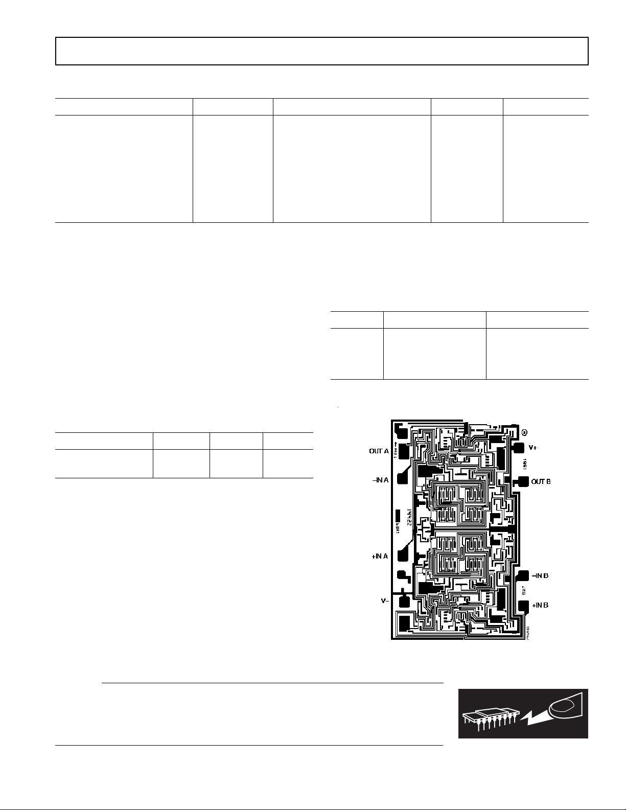
OUT A
–IN A
+IN A
V–
OUT B
–IN B
+IN B
V+
1
2
3
4
5
6
7
8
1
2
3
4
8
7
6
5
OP275
OUT B
–IN B
+IN B
V+OUT A
–IN A
+IN A
V–
a
FEATURES
Excellent Sonic Characteristics
Low Noise: 6 nV/√Hz
Low Distortion: 0.0006%
High Slew Rate: 22 V/s
Wide Bandwidth: 9 MHz
Low Supply Current: 5 mA
Low Offset Voltage: 1 mV
Low Offset Current: 2 nA
Unity Gain Stable
SOIC-8 Package
APPLICATIONS
High Performance Audio
Active Filters
Fast Amplifiers
Integrators
GENERAL DESCRIPTION
The OP275 is the first amplifier to feature the Butler Amplifier
front-end. This new front-end design combines both bipolar
and JFET transistors to attain amplifiers with the accuracy and
low noise performance of bipolar transistors, and the speed and
sound quality of JFETs. Total Harmonic Distortion plus Noise
equals that of previous audio amplifiers, but at much lower supply currents.
A very low l/f corner of below 6 Hz maintains a flat noise density
response. Whether noise is measured at either 30 Hz or 1 kHz,
it is only 6 nV/√
the OP275 its high slew rates to keep distortion low, even when
large output swings are required, and the 22 V/µs slew rate of
the OP275 is the fastest of any standard audio amplifier. Best of
all, this low noise and high speed are accomplished using less
than 5 mA of supply current, lower than any standard audio
amplifier.
Hz. The JFET portion of the input stage gives
Operational Amplifier
OP275*
PIN CONNECTIONS
8-Lead Narrow-Body SO 8-Lead Epoxy DIP
(S Suffix) (P Suffix)
Improved dc performance is also provided with bias and offset
currents greatly reduced over purely bipolar designs. Input offset voltage is guaranteed at 1 mV and is typically less than
200 µV. This allows the OP275 to be used in many dc coupled
or summing applications without the need for special selections
or the added noise of additional offset adjustment circuitry.
The output is capable of driving 600 Ω loads to 10 V rms while
maintaining low distortion. THD + Noise at 3 V rms is a low
0.0006%.
The OP275 is specified over the extended industrial (–40°C to
+85°C) temperature range. OP275s are available in both plastic
DIP and SOIC-8 packages. SOIC-8 packages are available in
2500 piece reels. Many audio amplifiers are not offered in
SOIC-8 surface mount packages for a variety of reasons; however, the OP275 was designed so that it would offer full performance in surface mount packaging.
*Protected by U.S. Patent No. 5,101,126.
REV. A
Information furnished by Analog Devices is believed to be accurate and
reliable. However, no responsibility is assumed by Analog Devices for its
use, nor for any infringements of patents or other rights of third parties
which may result from its use. No license is granted by implication or
otherwise under any patent or patent rights of Analog Devices.
One Technology Way, P.O. Box 9106, Norwood. MA 02062-9106, U.S.A.
Tel: 617/329-4700 Fax: 617/326-8703
© Analog Devices, Inc., 1995
Page 2

OP275–SPECIFICATIONS
ELECTRICAL CHARACTERISTICS
(@ VS = ⫾15.0 V, TA = +25ⴗC unless otherwise noted)
Parameter␣ Symbol Conditions Min Typ Max Units
AUDIO PERFORMANCE␣
THD + Noise V
Voltage Noise Density e
n
= 3 V rms,
IN
R
= 2 kΩ, f = 1 kHz 0.006 %
L
f = 30 Hz 7 nV/√Hz
f = 1 kHz 6 nV/√
Current Noise Density i
n
f = 1 kHz 1.5 pA/√Hz
Headroom THD + Noise ≤ 0.01%,
R
= 2 kΩ, VS = ±18 V >12.9 dBu
L
INPUT CHARACTERISTICS␣
Offset Voltage V
Input Bias Current I
Input Offset Current I
Input Voltage Range V
OS
B
OS
CM
Common-Mode Rejection Ratio CMRR V
Large Signal Voltage Gain A
VO
–40°C ≤ T
≤ +85°C 1.25 mV
A
VCM = 0 V 100 350 nA
V
= 0 V, –40°C ≤ TA ≤ +85°C 100 400 nA
CM
VCM = 0 V 2 50 nA
= 0 V, –40°C ≤ TA ≤ +85°C 2 100 nA
V
CM
–10.5 +10.5 V
= ±10.5 V,
CM
–40°C ≤ T
R
= 2 kΩ 250 V/mV
L
R
= 2 kΩ, –40°C ≤ TA ≤ +85°C 175 V/mV
L
= 600 Ω 200 V/mV
R
L
≤ +85°C 80 106 dB
A
1mV
Offset Voltage Drift ∆VOS/∆T2µV/°C
Hz
OUTPUT CHARACTERISTICS␣
R
Output Voltage Swing V
O
= 2 kΩ –13.5 ±13.9 +13.5 V
L
= 2 kΩ, –40°C ≤ TA ≤ +85°C –13 ±13.9 +13 V
R
L
R
= 600 Ω, VS = ±18 V +14, –16 V
L
POWER SUPPLY␣
Power Supply Rejection Ratio PSRR V
Supply Current I
Supply Voltage Range V
SY
S
= ±4.5 V to ±18 V 85 111 dB
S
V
= ±4.5 V to ±18 V,
S
–40°C ≤ T
V
= ±4.5 V to ±18 V, V
S
R
= ∞, –40°C ≤ TA ≤ +85°C45mA
L
= ±22 V, V
V
S
–40°C ≤ T
≤ +85°C80 dB
A
= 0 V, R
O
≤ +85°C 5.5 mA
A
= 0 V,
O
= ∞,
L
±4.5 ±22 V
DYNAMIC PERFORMANCE␣
Slew Rate SR R
Full-Power Bandwidth BW
P
= 2 kΩ 15 22 V/µs
L
Gain Bandwidth Product GBP 9 MHz
Phase Margin ø
m
Overshoot Factor V
Specifications subject to change without notice.
= 100 mV, AV = +1,
IN
R
= 600 Ω, C
L
= 100 pF 10 %
L
62 Degrees
kHz
–2–
REV. A
Page 3
OP275
WARNING!
ESD SENSITIVE DEVICE
WAFER TEST LIMITS
(@ VS = ⴞ15.0 V, TA = +25ⴗC unless otherwise noted)
Parameter Symbol Conditions Limit Units
Offset Voltage V
Input Bias Current I
Input Offset Current I
Input Voltage Range
1
OS
B
OS
V
CM
Common-Mode Rejection Ratio CMRR V
VCM = 0 V 350 nA max
VCM = 0 V 50 nA max
= ±10.5 V 80 dB min
CM
1mV max
±10.5 V min
Power Supply Rejection Ratio PSRR V = ±4.5 V to ±18 V 85 dB min
R
Large Signal Voltage Gain A
Output Voltage Range V
Supply Current I
NOTES
Electrical tests and wafer probe to the limits shown. Due to variations in assembly methods and normal yield loss, yield after packaging is not guaranteed for standard
product dice. Consult factory to negotiate specifications based on dice lot qualifications through sample lot assembly and testing.
1
Guaranteed by CMRR test.
Specifications subject to change without notice.
ABSOLUTE MAXIMUM RATINGS
Supply Voltage . . . . . . . . . . . . . . . . . . . . . . . . . . . . . . . . ±22 V
Input Voltage
Differential Input Voltage
2
. . . . . . . . . . . . . . . . . . . . . . . . . . . . . . . . ±22 V
2
. . . . . . . . . . . . . . . . . . . . . . . ±7.5 V
Output Short-Circuit Duration to GND
VO
O
SY
1
3
. . . . . . . . . Indefinite
Storage Temperature Range
P, S Package . . . . . . . . . . . . . . . . . . . . . . . . –65°C to +150°C
Operating Temperature Range
= 2 kΩ 250 V/mV min
L
R
= 10 kΩ±13.5 V min
L
VO = 0 V, R
= ∞ 5 mA max
L
ORDERING GUIDE
Model Temperature Range Package Option
OP275GP –40°C to +85°C 8-Pin Plastic DIP
OP275GS –40°C to +85°C 8-Pin SOIC
OP275GSR –40°C to +85°C SO-8 Reel, 2500 pcs.
OP275GBC +25°C DICE
OP275G . . . . . . . . . . . . . . . . . . . . . . . . . . . . –40°C to +85°C
Junction Temperature Range
P, S Package . . . . . . . . . . . . . . . . . . . . . . . . –65°C to +150°C
DICE CHARACTERISTICS
Lead Temperature Range (Soldering, 60 sec) . . . . . . . +300°C
Package Type θ
4
JA
θ
JC
Units
8-Pin Plastic DIP (P) 103 43 °C/W
8-Pin SOIC (S) 158 43 °C/W
NOTES
1
Absolute maximum ratings apply to both DICE and packaged parts, unless
otherwise noted.
2
For supply voltages greater than ±22 V, the absolute maximum input voltage is
equal to the supply voltage.
3
Shorts to either supply may destroy the device. See data sheet for full details.
4
θJA is specified for the worst case conditions, i.e., θ
for cerdip, P-DIP, and LCC packages; θ
board for SOIC package.
JA
is specified for device in socket
JA
is specified for device soldered in circuit
CAUTION
ESD (electrostatic discharge) sensitive device. Electrostatic charges as high as 4000 V readily
accumulate on the human body and test equipment and can discharge without detection.
Although the OP275 features proprietary ESD protection circuitry, permanent damage may
occur on devices subjected to high energy electrostatic discharges. Therefore, proper ESD
precautions are recommended to avoid performance degradation or loss of functionality.
REV. A
Die Size 0.070 × 0.108 in. (7,560 sq. mils)
Substrate is connected to V–
–3–
Page 4
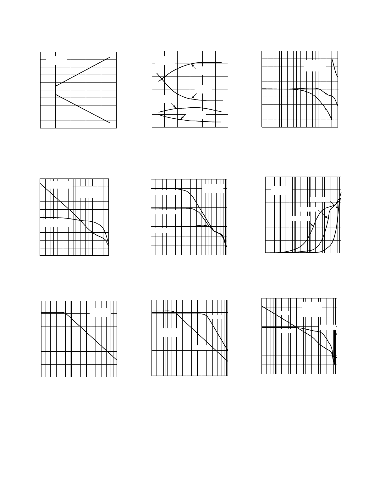
OP275–Typical Performance Curves
FREQUENCY – Hz
1M 10M
10k 100k
PHASE – Degrees
180
135
–180
90
45
0
–45
–90
–135
40
30
–40
20
10
0
–10
–20
–30
GAIN – dB
VS = ±15V
T
A
= +25°C
FREQUENCY – Hz
100
80
–60
1k 10k 100M
100k 1M 10M
60
40
20
0
–20
–40
0
PHASE – Degrees
45
90
135
180
225
270
VS = ±15V
R
L
= 2kΩ
T
A
= +25°C
OPEN-LOOP GAIN – dB
GAIN
PHASE
Øm= 58°
25
TA = +25°C
20
R
= 2kΩ
L
15
10
5
0
–5
–10
–15
OUTPUT VOLTAGE SWING – V
–20
–25
0 ±5 ±25
±10 ±15 ±20
SUPPLY VOLTAGE – V
+VOM
–VOM
Output Voltage Swing vs. Supply
Voltage
MARKER 15 309.059Hz
MAG (A/H) 60.115dB
60
50
40
30
20
MARKER 15 309.058Hz
PHASE (A/R 90.606Deg
10
GAIN – dB
0
–10
–20
10k 100k
VS = ±15V
TA = +25°C
135
90
45
0
–45
–90
1M 10M
FREQUENCY – Hz
OPEN-LOOP GAIN – V/mV
Open-Loop Gain vs. Temperature
PHASE – Degrees
1500
VS = ±15V
= ±10V
V
O
1250
1000
750
+GAIN
= 600Ω
R
L
500
250
0
–50 –25 100
50
40
A
30
20
A
10
0
A
–10
CLOSED-LOOP GAIN – dB
–20
–30
1k 10k 100M
0255075
TEMPERATURE – °C
= +100
VCL
= +10
VCL
= +1
VCL
100k 1M 10M
FREQUENCY – Hz
–GAIN
= 600Ω
R
L
+GAIN
R
L
–GAIN
= 2kΩ
R
L
= 2kΩ
VS = ±15V
= +25°C
T
A
Closed-Loop Gain and Phase, AV = +1
60
VS = ±15V
50
= +25°C
T
A
40
30
20
IMPEDANCE – Ω
10
0
100 1k 10M
A
VCL
FREQUENCY – Hz
A
= +1
VCL
A
= +10
VCL
= +100
10k 100k 1M
Open-Loop Gain, Phase vs. Frequency
120
100
80
60
40
20
COMMON-MODE REJECTION – dB
0
100 1k 10M10k 100k 1M
FREQUENCY – Hz
VS = ±15V
T
Common-Mode Rejection vs.
Frequency
= +25°C
A
Closed-Loop Gain vs. Frequency
120
100
80
VS = ±15V
= +25°C
T
A
60
40
20
POWER SUPPLY REJECTION – dB
0
10 100 1M
1k 10k 100k
FREQUENCY – Hz
+PSRR
–PSRR
Power Supply Rejection vs.
Frequency
–4–
Closed-Loop Output Impedance vs.
Frequency
Open-Loop Gain, Phase vs. Frequency
REV. A
Page 5

OP275
11
10
9
8
GAIN BANDWIDTH PRODUCT – MHz
7
–50 –25 100
TEMPERATURE – °C
Ø
m
GBW
0255075
Gain Bandwidth Product, Phase
Margin vs. Temperature
30
25
20
15
TA = +25°C
= ±15V
V
10
5
MAXIMUM OUTPUT SWING – V
0
S
= +1
A
VCL
= 2kΩ
R
L
1k 10k 10M
100k 1M
FREQUENCY – Hz
65
60
55
50
PHASE MARGIN – Degrees
40
100
OVERSHOOT – %
Small-Signal Overshoot vs. Load
Capacitance
5.0
4.5
4.0
3.5
SUPPLY CURRENT – mA
3.0
A
90
80
70
60
50
40
30
20
10
0
0 100 500
TA = +85°C
TA = +25°C
TA = –40°C
0 ±5 ±25
= +1
VCL
NEGATIVE EDGE
A
= +1
VCL
POSITIVE EDGE
VS = ±15V
= 2kΩ
R
L
V
= 100mV p-p
IN
200 300 400
LOAD CAPACITANCE – pF
±10 ±15
SUPPLY VOLTAGE – V
±20
16
14
–VOM
12
10
8
6
4
MAXIMUM OUTPUT SWING – V
2
0
100 1k 10k
+VOM
T
V
LOAD RESISTANCE – Ω
= +25°C
A
= ±15V
S
Maximum Output Voltage vs. Load
Resistance
120
110
100
90
80
70
60
50
40
30
ABSOLUTE OUTPUT CURRENT – mA
20
SINK
SOURCE
–50 –25 100
0255075
TEMPERATURE – °C
VS = ±15V
Maximum Output Swing vs.
Frequency
300
250
200
150
100
INPUT BIAS CURRENT – nA
50
0
–50 –25 100
TEMPERATURE – °C
VS = ±15V
0255075
Input Bias Current vs. Temperature
Supply Current vs. Supply Voltage
5
Hz
4
3
2
1
CURRENT NOISE DENSITY – pA/
10 100 100k1k
FREQUENCY – Hz
V
= ±15V
S
T = +25°C
A
Current Noise Density vs. Frequency
Short Circuit Current vs. Temperature
500
400
BASED ON 920 OP AMPS
300
UNITS
200
100
0
01 10
234 567 8 9
VS = ±15V
–40°C to +85°C
TCVOS – µV/°C
TCVOS Distribution
REV. A
–5–
Page 6

OP275–Typical Performance Curves
200
BASED ON 920 OP AMPS
160
120
UNITS
80
40
0
–300–200
–400
–500
INPUT OFFSET VOLTAGE – µV
–100
0 100 200
VS = ±15V
TA = +25°C
300
Input Offset (VOS) Distribution
40
VS = ±15V
35
R
= 2kΩ
L
30
= +25°C
T
A
25
20
15
SLEW RATE – V/µs
10
5
0
0.2.4.6.81.0
DIFFERENTIAL INPUT VOLTAGE – V
400
500
10
8
6
4
2
0
–2
STEP SIZE – V
–4
–6
–8
–10
0 100 900
+0.1%
–0.1%
200 300 400 500 600 700 800
SETTLING TIME – ns
+0.01%
–0.01%
Settling Time vs. Step Size
50
45
40
35
30
SLEW RATE – V/µs
25
20
0 100 500
–SR
+SR
CAPACITIVE LOAD – pF
Slew Rate vs. Capacitive Load
50
VS = ±15V
45
= 2kΩ
R
L
40
35
30
SLEW RATE – V/µs
25
20
–50 –25 100
TEMPERATURE – °C
–SR
+SR
0255075
TA = +25°C
= ±15V
V
S
200 300 400
Slew Rate vs. Differential Input Voltage
100
90
10
0%
5V
200ns
Negative Slew Rate
= 2 kΩ, VS = ±15 V, AV = +1
R
L
100
90
10
0%
50mV
100ns
Slew Rate vs. Temperature
100
90
10
0%
5V
200ns
Positive Slew Rate
= 2 kΩ, VS = ±15 V, AV = +1
R
L
CH A: 80.0 µV FS 10.0 µV/DIV
MKR: 6.23 nV/√Hz
2.5 kHz0 Hz
BW: 15.0 MHzMKR: 1 000 Hz
Small Signal Response
= 2 kΩ, VS = ±15 V, AV = +1
R
L
–6–
Voltage Noise Density vs. Frequency
= ±15 V
V
S
REV. A
Page 7

OP275
SUPPLY VOLTAGE – V
0.0001
0.001
THD – %
0
±17 ±22±18 ±19 ±20 ±21
0.01
0.1
RL = 600Ω
V
OUT
= 10 Vrms @ 1kHz
APPLICATIONS
Short Circuit Protection
The OP275 has been designed with inherent short circuit pro-
tection to ground. An internal 30 Ω resistor, in series with the
output, limits the output current at room temperature to I
= 40 mA and I
– = –90 mA, typically, with ±15 V supplies.
SC
SC
+
However, shorts to either supply may destroy the device when
excessive voltages or currents are applied. If it is possible for a
user to short an output to a supply, for safe operation, the out-
put current of the OP275 should be design-limited to ±30 mA,
as shown in Figure 1.
Total Harmonic Distortion
Total Harmonic Distortion + Noise (THD + N) of the OP275
is well below 0.001% with any load down to 600 Ω. However,
this is dependent upon the peak output swing. In Figure 2 it is
seen that the THD + Noise with 3 V rms output is below
0.001%. In the following Figure 3, THD + Noise is below
0.001% for the 10 kΩ and 2 kΩ loads but increases to above
0.1% for the 600␣ Ω load condition. This is a result of the output
swing capability of the OP275. Notice the results in Figure 4,
showing THD vs. V
(V rms). This figure shows that the THD
IN
+ Noise remains very low until the output reaches 9.5 volts rms.
This performance is similar to competitive products.
R
FB
0.010
VS = ±18V
= 600Ω
R
L
0.001
THD + NOISE – %
0.0001
0.5 1 10
OUTPUT SWING – V rms
Figure 4. Headroom, THD + Noise vs. Output Amplitude
(V rms); R
= 600 Ω, V
LOAD
= ±18 V
SUP
The output of the OP275 is designed to maintain low harmonic
distortion while driving 600 Ω loads. However, driving 600 Ω
loads with very high output swings results in higher distortion if
clipping occurs. A common example of this is in attempting to
drive 10 V rms into any load with ±15 volt supplies. Clipping
will occur and distortion will be very high.
To attain low harmonic distortion with large output swings,
supply voltages may be increased. Figure 5 shows the perfor-
mance of the OP275 driving 600␣ Ω loads with supply voltages
varying from ±18 volts to ±20 volts. Notice that with ±18 volt
supplies the distortion is fairly high, while with ±20 volt supplies
it is a very low 0.0007%.
FEEDBACK
X
R
A1
332Ω
A1 = 1/2 OP275
V
OUT
Figure 1. Recommended Output Short Circuit Protection
0.010
RL = 600Ω, 2k, 10k
VS = ±15V
= 3V rms
V
IN
= +1
A
V
THD + NOISE – %
0.001
0.0005
20 100 1k 10k 20k
Figure 2. THD + Noise vs. Frequency vs. R
1
0.1
0.010
THD + NOISE – %
0.001
0.0001
20 100 1k 10k 20k
Figure 3. THD + Noise vs. R
±
18 V Supplies
FREQUENCY – Hz
600Ω
2k
FREQUENCY – Hz
LOAD
AV = +1
VS = ±18V
= 10V rms
V
IN
80kHz FILTER
10k
; VIN =10 V rms,
LOAD
Figure 5. THD + Noise vs. Supply Voltage
Noise
The voltage noise density of the OP275 is below 7 nV/√Hz from
30 Hz. This enables low noise designs to have good performance throughout the full audio range. Figure 6 shows a typical
OP275 with a 1/f corner at 2.24 Hz.
CH A: 80.0 µV FS 10.0 µV/DIV
0 Hz
MKR: 45.6 µV/√Hz
10 Hz
BW: 0.145 HzMKR: 2.24 Hz
Figure 6. 1/f Noise Corner, VS = ±15 V, AV = 1000
REV. A
–7–
Page 8

OP275
Noise Testing
For audio applications the noise density is usually the most important noise parameter. For characterization the OP275 is
tested using an Audio Precision, System One. The input signal
to the Audio Precision must be amplified enough to measure it
accurately. For the OP275 the noise is gained by approximately
1020 using the circuit shown in Figure 7. Any readings on the
Audio Precision must then be divided by the gain. In implementing this test fixture, good supply bypassing is essential.
100Ω
909Ω
100Ω
A
OP275
B
909Ω
OP37
100Ω
909Ω
OP37
OUTPUT
4.42kΩ
490Ω
Figure 7. Noise Test Fixture
Input Overcurrent Protection
The maximum input differential voltage that can be applied to
the OP275 is determined by a pair of internal Zener diodes connected across its inputs. They limit the maximum differential in-
put voltage to ±7.5 V. This is to prevent emitter-base junction
breakdown from occurring in the input stage of the OP275
when very large differential voltages are applied. However, in order to preserve the OP275’s low input noise voltage, internal resistances in series with the inputs were not used to limit the
current in the clamp diodes. In small signal applications, this is
not an issue; however, in applications where large differential
voltages can be inadvertently applied to the device, large transient currents can flow through these diodes. Although these di-
odes have been designed to carry a current of ±5 mA, external
resistors as shown in Figure 8 should be used in the event that
the OP275’s differential voltage were to exceed ±7.5 V.
1.4kΩ
2
–
6
1.4kΩ
OP275
3
+
Figure 8. Input Overcurrent Protection
Output Voltage Phase Reversal
Since the OP275’s input stage combines bipolar transistors for
low noise and p-channel JFETs for high speed performance, the
output voltage of the OP275 may exhibit phase reversal if either
of its inputs exceed its negative common-mode input voltage.
This might occur in very severe industrial applications where a
sensor, or system, fault might apply very large voltages on the
inputs of the OP275. Even though the input voltage range of the
OP275 is ±10.5 V, an input voltage of approximately –13.5 V
will cause output voltage phase reversal. In inverting amplifier
configurations, the OP275’s internal 7.5 V input clamping diodes will prevent phase reversal; however, they will not prevent
this effect from occurring in noninverting applications. For these
applications, the fix is a simple one and is illustrated in Figure 9.
A 3.92 kΩ resistor in series with the noninverting input of the
OP275 cures the problem.
R
FB*
V
V
IN
R
3.92kΩ
IS OPTIONAL
*R
FB
S
R
2kΩ
L
OUT
Figure 9. Output Voltage Phase Reversal Fix
Overload, or Overdrive, Recovery
Overload, or overdrive, recovery time of an operational amplifier
is the time required for the output voltage to recover to a rated
output voltage from a saturated condition. This recovery time is
important in applications where the amplifier must recover
quickly after a large abnormal transient event. The circuit
shown in Figure 10 was used to evaluate the OP275’s overload
recovery time. The OP275 takes approximately 1.2 µs to recover
to V
= +10 V and approximately 1.5 µs to recover to V
OUT
OUT
=
–10 V.
R2
10kΩ
2
3
A1
1
R
2.43kΩ
V
OUT
L
V
IN
4V p-p
@100Hz
R1
1kΩ
R
S
909Ω
A1 = 1/2 OP275
Figure 10.␣ Overload Recovery Time Test Circuit
Measuring Settling Time
The design of OP275 combines high slew rate and wide gainbandwidth product to produce a fast-settling (t
< 1 µs) ampli-
S
fier for 8- and 12-bit applications. The test circuit designed to
measure the settling time of the OP275 is shown in Figure 11.
This test method has advantages over false-sum node techniques in that the actual output of the amplifier is measured, instead of an error voltage at the sum node. Common-mode
settling effects are exercised in this circuit in addition to the slew
rate and bandwidth effects measured by the false-sum-node
method. Of course, a reasonably flat-top pulse is required as the
stimulus.
The output waveform of the OP275 under test is clamped by
Schottky diodes and buffered by the JFET source follower. The
signal is amplified by a factor of ten by the OP260 and then
Schottky-clamped at the output to prevent overloading the
oscilloscope’s input amplifier. The OP41 is configured as a fast
integrator which provides overall dc offset nulling.
High Speed Operation
As with most high speed amplifiers, care should be taken with
supply decoupling, lead dress, and component placement. Recommended circuit configurations for inverting and noninverting
applications are shown in Figures 12 and Figure 13.
–8–
REV. A
Page 9

0.1µF
+15V
16–20V
–+
0.1µF
0.1µF
+
16–20V
±5V
10µF
+
+15V
R
V+
DUT
V–
–
1kΩ
1N4148
L
D1 D2
–15V
15kΩ
2N4416
2N2222A
1/2 OP260AJ
R
F
2kΩ
R
G
222Ω
SCHOTTKY DIODES D1–D4 ARE
HEWLETT-PACKARD HP5082-2835
IC1 IS 1/2 OP260AJ
IC2 IS PMI OP41EJ
Figure 11.␣ OP275’s Settling Time Test Fixture
1kΩ
10kΩ
750Ω
D3
10kΩ
D4
1µF
IC2
OUTPUT
(TO SCOPE)
C
FB
R
FB
OP275
2
8
1/2
–15V
1
4
0.1µF
OP275
10µF
+
3
V
IN
R
2kΩ
V
OUT
L
Figure 12. Unity Gain Follower
+15V
10µF
+
V
IN
2.49kΩ
4.99kΩ
0.1µF
2
3
0.1µF
1/2
OP275
–15V
8
4
10µF
10pF
4.99kΩ
1
+
2kΩ
V
OUT
Figure 13. Unity Gain Inverter
In inverting and noninverting applications, the feedback resistance forms a pole with the source resistance and capacitance
and CS) and the OP275’s input capacitance (CIN), as shown
(R
S
in Figure 14. With R
and RF in the kilohm range, this pole can
S
create excess phase shift and even oscillation. A small capacitor,
, in parallel and RFB eliminates this problem. By setting R
C
FB
S
(CS + CIN) = RFBCFB, the effect of the feedback pole is completely removed.
R
S
C
S
C
IN
V
OUT
Figure 14. Compensating the Feedback Pole
Attention to Source Impedances Minimizes Distortion
Since the OP275 is a very low distortion amplifier, careful attention should be given to source impedances seen by both inputs.
As with many FET-type amplifiers, the p-channel JFETs in the
OP275’s input stage exhibit a gate-to-source capacitance that
varies with the applied input voltage. In an inverting configuration, the inverting input is held at a virtual ground and, as such,
does not vary with input voltage. Thus, since the gate-to-source
voltage is constant, there is no distortion due to input capacitance modulation. In noninverting applications, however, the
gate-to-source voltage is not constant. The resulting capacitance
modulation can cause distortion above 1 kHz if the input im-
pedance is > 2 kΩ and unbalanced.
Figure 15 shows some guidelines for maximizing the distortion
performance of the OP275 in noninverting applications. The
best way to prevent unwanted distortion is to ensure that the
parallel combination of the feedback and gain setting resistors
(R
and R
F
) is less than 2 kΩ. Keeping the values of these resis-
G
tors small has the added benefits of reducing the thermal noise
R
G
R
V
IN
S*
R
F
0P275
* RS = RG//RF IF RG//RF > 2kΩ
FOR MINIMUM DISTORTION
V
OUT
Figure 15. Balanced Input Impedance to Minimize
Distortion in Noninverting Amplifier Circuits
REV. A
–9–
Page 10

OP275
of the circuit and dc offset errors. If the parallel combination of
R
and R
F
is larger than 2␣ kΩ, then an additional resistor, R
G
,
S
should be used in series with the noninverting input. The value
is determined by the parallel combination of RF and RG to
of R
S
maintain the low distortion performance of the OP275.
Driving Capacitive Loads
The OP275 was designed to drive both resistive loads to 600 Ω
and capacitive loads of over 1000 pF and maintain stability.
While there is a degradation in bandwidth when driving capacitive loads, the designer need not worry about device stability.
The graph in Figure 16 shows the 0 dB bandwidth of the OP275
with capacitive loads from 10 pF to 1000 pF.
10
9
8
7
6
5
4
BANDWIDTH – MHz
3
2
1
0
0 200 400 600 800 1000
Figure 16. Bandwidth vs. C
– pF
C
LOAD
LOAD
High Speed, Low Noise Differential Line Driver
The circuit of Figure 17 is a unique line driver widely used in
industrial applications. With ±18 V supplies, the line driver can
deliver a differential signal of 30 V p-p into a 2.5 kΩ load. The
high slew rate and wide bandwidth of the OP275 combine to
yield a full power bandwidth of 130 kHz while the low noise
front end produces a referred-to-input noise voltage spectral
density of 10 nV/√
3
V
IN
2
A1 = 1/2 OP275
A2, A3 = 1/2 OP275
R3
GAIN =
R1
SET R2, R4, R5 = R1 AND R6, R7, R8 = R3
Hz.
R3
2k
2
A2
3
R1
2k
1
A1
R2
2k
R4
2k
R5
2k
R6
2k
6
A3
5
R9
50
1
R11
10k
R12
1k
P1
1k
R7
2k
R10
50
7
R8
2k
V
O2
V
O1
– VO1 = V
V
O2
IN
Figure 17. High Speed, Low Noise Differential Line Driver
importance. Like the transformer based design, either output
can be shorted to ground for unbalanced line driver applications
without changing the circuit gain of 1. Other circuit gains can be
set according to the equation in the diagram. This allows the
design to be easily set to noninverting, inverting, or differential
operation.
A 3-Pole, 40 kHz Low-Pass Filter
The closely matched and uniform ac characteristics of the
OP275 make it ideal for use in GIC (Generalized Impedance
Converter) and FDNR (Frequency-Dependent Negative Resistor) filter applications. The circuit in Figure 18 illustrates a linear-phase, 3-pole, 40 kHz low-pass filter using an OP275 as an
inductance simulator (gyrator). The circuit uses one OP275 (A2
and A3) for the FDNR and one OP275 (A1 and A4) as an input
buffer and bias current source for A3. Amplifier A4 is configured in a gain of 2 to set the pass band magnitude response to
0 dB. The benefits of this filter topology over classical approaches are that the op amp used in the FDNR is not in the
signal path and that the filter’s performance is relatively insensitive to component variations. Also, the configuration is such that
large signal levels can be handled without overloading any of the
the filter’s internal nodes. As shown in Figure 19, the OP275’s
symmetric slew rate and low distortion produce a clean, wellbehaved transient response.
R1
95.3kΩ
2
A1
3
V
IN
1
A2
C1
2200pF
1
R2
R6
787Ω
4.12kΩ
A3
2200pF
7
C4
100kΩ
A1, A4 = 1/2 OP275
A2, A3 = 1/2 OP275
C2
2200pF
1.82kΩ
2
2200pF
1.87kΩ
1.82kΩ
C3
3
5
6
R3
R4
R5
5
7
A4
6
R7
R8
R9
1kΩ
1kΩ
V
OUT
Figure 18. A 3-Pole, 40 kHz Low-Pass Filter
100
90
V
OUT
10Vp-p
10kHz
10
0%
SCALE: VERTICAL–2V/ DIV
HORIZONTAL–10µs/ DIV
The design is a transformerless, balanced transmission system
where output common-mode rejection of noise is of paramount
–10–
Figure 19. Low-Pass Filter Transient Response
REV. A
Page 11

OP275
OP275 SPICE Model
*
* Node assignments
* noninverting input
* inverting input
* positive supply
* negative supply
* output
*
*
.SUBCKT OP275 1 2 99 50 34
*
* INPUT STAGE & POLE AT 100 MHz
*
R3 5 51 2.188
R4 6 51 2.188
CIN 1 2 3.7E-12
CM1 1 98 7.5E-12
CM2 2 98 7.5E-12
C2 5 6 364E-12
I1 97 4 100E-3
IOS 1 2 1E-9
EOS 9 3 POLY(1) 26 28 0.5E-3 1
Q1 5 2 7 QX
Q2 6 9 8 QX
R5 7 4 1.672
R6 8 4 1.672
D1 2 36 DZ
D2 1 36 DZ
EN 3 1 10 0 1
GN1 0 2 13 0 1E-3
GN2 0 1 16 0 1E-3
*
EREF 98 0 28 0 1
EP 97 0 99 0 1
EM 51 0 50 0 1
*
* VOLTAGE NOISE SOURCE
*
DN1 35 10 DEN
DN2 10 11 DEN
VN1 35 0 DC 2
VN2 0 11 DC 2
*
* CURRENT NOISE SOURCE
*
DN3 12 13 DIN
DN4 13 14 DIN
VN3 12 0 DC 2
VN4 0 14 DC 2
*
* CURRENT NOISE SOURCE
*
DN5 15 16 DIN
DN6 16 17 DIN
VN5 15 0 DC 2
VN6 0 17 DC 2
*
* GAIN STAGE & DOMINANT POLE AT 32 Hz
*
R7 18 98 1.09E6
C3 18 98 4.55E-9
G1 98 18 5 6 4.57E-1
V2 97 19 1.35
V3 20 51 1.35
D3 18 19 DX
D4 20 18 DX
*
* POLE/ZERO PAIR AT 1.5 MHz/2.7 MHz
*
R8 21 98 1E-3
R9 21 22 1.25E-3
C4 22 98 47.2E-12
G2 98 21 18 28 1E-3
*
* POLE AT 100 MHz
*
R10 23 98 1
C5 23 98 1.59E-9
G3 98 23 21 28 1
*
* POLE AT 100 MHz
*
R11 24 98 1
C6 24 98 1.59E-9
G4 98 24 23 28 1
*
* COMMON-MODE GAIN NETWORK WITH ZERO AT
1 kHz
*
R12 25 26 1E6
C7 25 26 1.5915E-12
R13 26 98 1
E2 25 98 POLY(2) 1 98 2 98 0 2.50 2.50
*
* POLE AT 100 MHz
*
R14 27 98 1
C8 27 98 1.59E-9
G5 98 27 24 28 1
*
* OUTPUT STAGE
*
R15 28 99 100E3
R16 28 50 100E3
C9 28 50 1E-6
ISY 99 50 1.85E-3
R17 29 99 100
R18 29 50 100
L2 29 34 1E-9
G6 32 50 27 29 10E-3
G7 33 50 29 27 10E-3
G8 29 99 99 27 10E-3
G9 50 29 27 50 10E-3
V4 30 29 1.3
V5 29 31 3.8
F1 29 0 V4 1
F2 0 29 V5 1
D5 27 30 DX
D6 31 27 DX
D7 99 32 DX
D8 99 33 DX
D9 50 32 DY
D10 50 33 DY
*
* MODELS USED
*
.MODEL QX PNP(BF=5E5)
.MODEL DX D(IS=1E-12)
.MODEL DY D(IS=1E-15 BV=50)
.MODEL DZ D(IS=1E-15 BV=7.0)
.MODEL DEN D(IS=1E-12 RS=4.35K KF=1.95E-15 AF=1)
.MODEL DIN D(IS=1E-12 RS=268 KF=1.08E-15 AF=1)
.ENDS
REV. A
–11–
Page 12

OP275
OUTLINE DIMENSIONS
Dimensions shown in inches and (mm).
0.2440 (6.20)
0.2284 (5.80)
0.0098 (0.25)
0.0040 (0.10)
SEATING
PLANE
8-Lead Narrow-Body SOIC
(S Suffix)
0.1968 (5.00)
0.1890 (4.80)
85
0.1574 (4.00)
0.1497 (3.80)
41
0.0688 (1.75)
PIN 1
0.0500
(1.27)
BSC
0.0532 (1.35)
0.0192 (0.49)
0.0138 (0.35)
0.0098 (0.25)
0.0075 (0.19)
0.0196 (0.50)
0.0099 (0.25)
8°
0°
x 45°
0.0500 (1.27)
0.0160 (0.41)
0.210
(5.33)
MAX
0.160 (4.06)
0.115 (2.93)
0.022 (0.558)
0.014 (0.356)
8-Lead Epoxy DIP
(P Suffix)
0.430 (10.92)
0.348 (8.84)
8
5
0.280 (7.11)
14
PIN 1
0.100
(2.54)
BSC
0.240 (6.10)
0.060 (1.52)
0.015 (0.38)
0.070 (1.77)
0.045 (1.15)
0.130
(3.30)
MIN
SEATING
PLANE
C1652a–2–7/95
0.325 (8.25)
0.300 (7.62)
0.195 (4.95)
0.115 (2.93)
0.015 (0.381)
0.008 (0.204)
–12–
PRINTED IN U.S.A.
REV. A
 Loading...