

Page 1
8
7
6
5
1
2
3
4
OUT A
–IN A
V+
OUT B
–IN B+IN A
+IN B
V–
+–+
–
B
A
16
15
14
13
12
11
10
9
1
2
3
4
5
6
7
8
NC = NO CONNECT
NC
–IN A
NC
+IN A
NC
NC
OUT B
NC
–IN B
NC
OUT A
V+
V–
NC
+IN B
NC
High-Speed, Dual
a
FEATURES
m
Excellent Speed: 8.5 V/
Fast Settling (0.01%): 2
Unity-Gain Stable
High-Gain Bandwidth: 5 MHz Typ
Low Input Offset Voltage: 200
Low Offset Voltage Drift: 21
High Gain: 400 V/mV Min
Outstanding CMR: 106 dB Min
Industry Standard 8-Pin Dual Pinout
Available in Die Form
GENERAL DESCRIPTION
The OP271 is a unity-gain stable monolithic dual op amp
featuring excellent speed, 8.5 V/ms typical, and fast settling
time, 2 ms typical to 0. 01%. The OP271 has a gain bandwidth
of 5 MHz with a high phase margin of 62∞.
Input offset voltage of the OP271 is under 200 mV with input
offset voltage drift below 2 mV/∞C, guaranteed over the full
military temperature range. Open-loop gain exceeds 400,000
into a 10 kW load ensuring outstanding gain accuracy and
linearity. The input bias current is under 20 nA limiting
errors due to source resistance. The OP271’s outstanding
CMR, over 106 dB, and low PSRR, under 5.6 mV/V, reduce
errors caused by ground noise and power supply fluctuations.
In addition, the OP27l exhibits high CMR and PSRR over a
wide frequency range, further improving system accuracy.
s Typ
m
s Typ
m
mV/∞
V Max
C Max
Operational Amplifier
OP271
PIN CONNECTIONS
16-Pin SOL
(S-Suffix)
Epoxy Mini-DIP
(P-Suffix)
8-Pin Hermetic DIP
(Z-Suffix)
+IN–IN
REV. A
Information furnished by Analog Devices is believed to be accurate and
reliable. However, no responsibility is assumed by Analog Devices for its
use, nor for any infringements of patents or other rights of third parties that
may result from its use. No license is granted by implication or otherwise
under any patent or patent rights of Analog Devices.
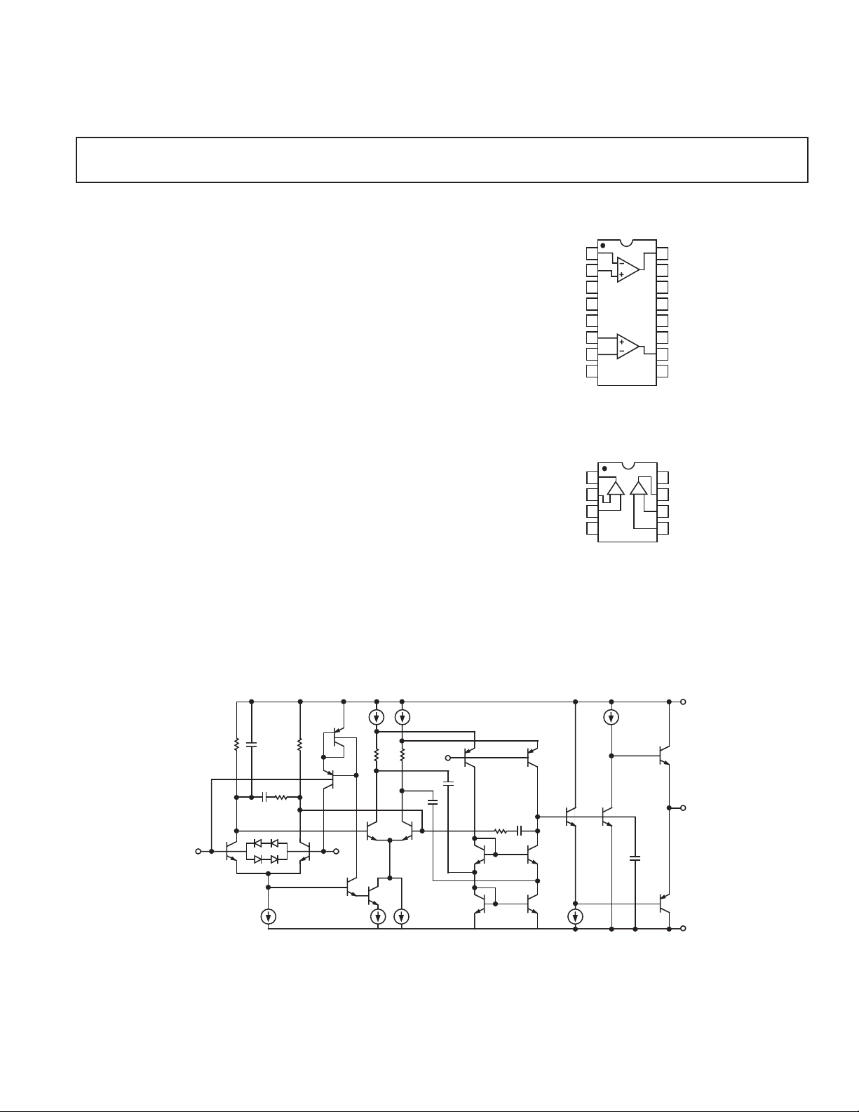
Figure 1. Simplified Schematic
(One of the two amplifiers is shown.)
V+
BIAS
OUT
V–
One Technology Way, P.O. Box 9106, Norwood, MA 02062-9106, U.S.A.
Tel: 781/329-4700 www.analog.com
Fax: 781/326-8703 © Analog Devices, Inc., 2002
Page 2

OP271–SPECIFICATIONS
ELECTRICAL CHARACTERISTICS
(VS = ±15 V, TA = 25∞C, unless otherwise noted.)
OP271A/E OP271F OP271G
Parameter Symbol Conditions Min Typ Max Min Typ Max Min Typ Max Unit
INPUT OFFSET
VOLTAGE V
OS
75 200 150 300 200 400 mV
INPUT OFFSET
CURRENT I
OS
VCM = 0 V 1 10 4 15 7 20 nA
INPUT BIAS
CURRENT I
B
VCM = 0 V 4 20 6 40 12 60 nA
INPUT NOISE
VOLTAGE
DENSITY e
n
LARGE-SIGNAL V
VOLTAGE A
VO
fO = 1 kHz 7.6 7.6 7.6 nV/Hz
= ± 10 V
O
RL = 10 kW 400 650 300 500 250 400 V/mV
GAIN RL = 2 kW 300 500 200 300 175 250 V/mV
INPUT VOLTAGE
RANGE IVR ± 12 ±12.5 ± 12 ±12.5 ± 12 ±12.5 V
OUTPUT
VOLTAGE SWING V
O
R
2 kW±12 ±13 ±12 ±13 ±12 ± 13 V
L ≥
COMMON-MODE
REJECTION CMR V
= ± 12 V 106 120 100 115 90 105 dB
CM
POWER SUPPLY
REJECTION PSRR VS = ± 4.5 V 0.6 3.2 1.8 5.6 2.4 7.0 mV/V
RATIO to ± 18 V
SLEW RATE SR 5.5 8.5 5.5 8.5 5.5 8.5 V/ms
PHASE MARGIN u
m
AV = +1 62 62 62 degrees
SUPPLY CURRENT
(ALL AMPLIFIERS) I
SY
No Load 4 5 6.5 4.5 6.5 4.5 6.5 mA
GAIN
BANDWIDTH
PRODUCT GBW 5 5 5 MHz
CHANNEL CS V
= 20 V
O
125 175 125 175 175 dB
p-p
SEPARATION fO = 10 Hz 125 175 125 175 175 dB
INPUT
CAPACITANCE C
IN
333pF
INPUT
RESISTANCE
DIFFERENTIAL MODE R
IN
0.4 0.4 0.4 MW
INPUT
RESISTANCE
COMMON
MODE R
SETTLING TIME t
INCM
S
AV = +1,
20 20 20 GW
10 V Step
to 0.01% 2 2 2 ms
NOTES
1
Guaranteed by CMR test.
2
Guaranteed but not 100% tested.
–2–
REV. A
Page 3

OP271
ELECTRICAL CHARACTERISTICS
(VS = ±15 V, –55∞C £ TA £ 125∞C for OP271A, unless otherwise noted.)
OP271A
Parameter Symbol Conditions Min Typ Max Unit
INPUT OFFSET VOLTAGE V
OS
115 400 mV
AVERAGE INPUT OFFSET
VOLTAGE DRIFT TCV
INPUT OFFSET CURRENT I
OS
OS
VCM = 0 V 1.5 30 nA
0.4 2 mV/∞C
INPUT BIAS CURRENT IB VCM = 0 V 7 60 nA
LARGE-SIGNAL VOLTAGE A
VO
GAIN R
VO = ± 10 V
= 10 kW 300 600 V/mV
L
RL = 2 kW 200 500 V/mV
INPUT VOLTAGE RANGE
OUTPUT VOLTAGE SWING V
1
IVR ± 12 ±12.5 V
O
RL ≥ 2 kW±12 ±13 V
COMMON-MODE REJECTION CMR VCM = ± 12 V 100 120 dB
POWER SUPPLY REJECTION
RATIO PSRR VS = ± 4.5 V to ±18 V 1.0 5.6 mV/V
SUPPLY CURRENT
(ALL AMPLIFIERS) I
NOTE
1
Guaranteed by CMR test.
SY
No Load 5.3 75 mA
ELECTRICAL CHARACTERISTICS
(VS = ±15 V, –40∞C £ TA £ +85∞C, unless otherwise noted.)
OP271A/E OP271F OP271G
Parameter Symbol Conditions Min Typ Max Min Typ Max Min Typ Max Unit
INPUT OFFSET
VOLTAGE V
OS
100 330 215 560 300 700 mV
AVERAGE INPUT
OFFSET
VOLTAGE DRIFT TCV
OS
0.4 2 1 4 2.0 5 mV/∞C
INPUT OFFSET
CURRENT I
OS
VCM = 0 V 1 30 5 40 15 50 nA
INPUT BIAS
CURRENT I
LARGE-SIGNAL A
B
VO
VOLTAGE GAIN R
VCM = 0 V 6 60 10 70 15 80 nA
VO = ± 10 V
= 10 kW 300 600 200 500 150 400 V/mV
L
RL = 2 kW 200 500 100 400 90 300 V/mV
INPUT VOLTAGE
RANGE
1
IVR ±12 ±12.5 ± 12 ± 12.5 ± 12 ± 12.5 V
OUTPUT
VOLTAGE SWING V
O
RL ≥ 2 kW±12 ± 13 ± 12 ±13 ±12 ± 13 V
COMMON-MODE
REJECTION CMR VCM = ± 12 V 100 120 94 115 90 100 dB
POWER SUPPLY
REJECTION PSRR VS = ± 4.5 V 0.7 5.6 51.8 10 2.0 15 mV/V
RATIO to ± 18 V
SUPPLY CURRENT
(ALL AMPLIFIERS) I
NOTE
1
Guaranteed by CMR test.
SY
No Load 5.2 7.2 5.2 7.2 5.2 7.2 mA
REV. A
–3–
Page 4
OP271
WARNING!
ESD SENSITIVE DEVICE
(Continued from Page 1)
The OP271 offers outstanding dc and ac matching between channels. This is especially valuable for applications such as multiple
gain blocks, high-speed instrumentation and amplifiers, buffers
and active filters.
The OP271 conforms to the industry standard, 8-pin dual op amp
pinout. It is pin compatible with the TL072, TL082, LF412,
and 1458/1558 dual op amps and can be used to significantly
improve systems using these devices.
For applications requiring lower voltage noise, see the OP270.
For a quad version of the OP271, see the OP471.
ABSOLUTE MAXIMUM RATINGS
Supply Voltage . . . . . . . . . . . . . . . . . . . . . . . . . . . . . . . ± 18 V
Differential Input Voltage
Differential Input Current
2
. . . . . . . . . . . . . . . . . . . . . . ± 1.0 V
2
. . . . . . . . . . . . . . . . . . . . ± 25 mA
1
Input Voltage . . . . . . . . . . . . . . . . . . . . . . . . . Supply Voltage
Output Short-Circuit Duration . . . . . . . . . . . . . . Continuous
Storage Temperature Range . . . . . . . . . . . . –65∞C to +150∞C
Lead Temperature (Soldering, 60 sec) . . . . . . . . . . . . 300∞C
Junction Temperature (Tj) . . . . . . . . . . . . . –65∞C to +150∞C
Operating Temperature Range
OP271A . . . . . . . . . . . . . . . . . . . . . . . . . . . –55∞C to +125∞C
OP271E, OP271F, OP271G . . . . . . . . . . . –40∞C to +85∞C
Package Type
3
jA
jC
Unit
8-Pin Hermetic DIP (Z) 134 12 ∞C/W
8-Pin Plastic DIP (P) 96 37 ∞C/W
8-Pin SOIC (S) 92 27 ∞C/W
NOTES
1
Absolute maximum ratings apply to packaged parts, unless otherwise noted.
2
The OP271’s inputs are protected by back-to-back diodes. Current limiting
resistors are not used in order to achieve low-noise performance. If differential
voltage exceeds ± 1.0 V, the input current should be limited to ± 25 mA.
3
jA is specified for worst case mounting conditions, i.e.,
device in socket for CERDIP and P-DIP packages; jA is specified for device
soldered to printed circuit board for SOIC package.
is specified for
jA
ORDERING GUIDE
Package
= 25∞C Operating
T
A
V
Max CERDIP Temperature
OS
(mV) 8-Pin Plastic Range
200 *OP271AZ MIL
200 *OP271EZ XND
300 *OP271FZ XND
400 OP271GP XND
400 *OP271GS XND
*Not for new design, obsolete April 2002.
CAUTION
ESD (electrostatic discharge) sensitive device. Electrostatic charges as high as 4000 V readily
accumulate on the human body and test equipment and can discharge without detection. Although
the OP271 features proprietary ESD protection circuitry, permanent damage may occur on devices
subjected to high-energy electrostatic discharges. Therefore, proper ESD precautions are
recommended to avoid performance degradation or loss of functionality.
–4–
REV. A
Page 5

Typical Performance Characteristics–
OP271
100
40
20
10
5
4
3
2
VOLTAGE NOISE DENSITY – nV/ Hz
1
1
1/f CORNER = 40Hz
10
FREQUENCY – Hz
TA = 25C
V
= 15V
S
1k100
TPC 1. Voltage Noise Density vs.
Frequency
10.0
1.0
1/f CORNER = 40Hz
CURRENT NOISE DENSITY – pA/ Hz
0.1
10 1k100
FREQUENCY – Hz
TA = 25C
= 15V
V
S
10k
25
= 25C
T
A
20
15
10
VOLTAGE NOISE DENSITY – nV/ Hz
5
0
5
SUPPLY VOLTAGE – Volts
10
AT 10Hz
AT 1kHz
15 20
TPC 2. Voltage Noise Density vs.
Supply Voltage
120
VS = 15V
100
80
60
40
20
INPUT OFFSET VOLTAGE – V
0
–20
TEMPERATURE – C
1251007550250–25–50–75
0.1
TA = 25C
V
= 15V
S
V
= 10V
p-p
O
RL = 2k
0.01
TOTAL HARMONIC DISTORTION – %
0.001
10
100 10k1k
FREQUENCY – Hz
AV = 100
AV = 10
AV = 1
TPC 3. Total Harmonic Distortion vs.
Frequency
10
T
= 25C
9
A
= 15V
V
S
8
7
6
5
4
3
2
CHANGE IN OFFSET VOLTAGE – V
1
0
01 5
234
TIME – Minutes
TPC 4. Current Noise Density vs.
Frequency
10
VS = 15V
VCM = 0V
8
6
4
2
INPUT BIAS CURRENT – nA
0
–2
–75
–50 –25 0 25 5075100125
TEMPERATURE – C
TPC 7. Input Bias Current vs.
Temperature
TPC 5. Input Offset Voltage vs.
Temperature
5
4
3
2
1
0
–1
–2
–3
INPUT OFFSET CURRENT – nA
–4
–5
–75 –50 –25 0 25 50 75 100 125
TEMPERATURE – C
TPC 8. Input Offset Current vs.
Temperature
TPC 6. Warm-Up Offset Voltage Drift
7
TA = 25C
VS = 15V
6
5
4
INPUT BIAS CURRENT – nA
3
2
–12.5 –7.5 0–2.5 2.5 7.5
COMMON MODE VOLTAGE – Volts
12.5
TPC 9. Input Bias Current vs.
Common-Mode Voltage
REV. A
–5–
Page 6

OP271
130
120
110
100
90
80
70
60
CMR – dB
50
40
30
TA = 25C
20
V
= 15V
S
10
1
FREQUENCY – Hz
10k1k10 100
TPC 10. CMR vs. Frequency
140
120
100
80
60
PSR – dB
40
20
+PSR
–PSR
100k
TA = 25C
1M
7
6
TA = +125C
5
4
TOTAL SUPPLY CURRENT – mA
3
0
5 20
SUPPLY VOLTAGE – Volts
TA = +25C
TA = –55C
10 15
TPC 11. Total Supply Current vs.
Supply Voltage
140
120
100
80
60
40
OPEN-LOOP GAIN – dB
20
TA = 25C
V
= 15V
S
7
VS = 15V
6
5
4
TOTAL SUPPLY CURRENT – mA
3
TEMPERATURE – C
1007550250–25–50–75
TPC 12. Total Supply Current vs.
Temperature
80
60
40
20
CLOSED-LOOP GAIN – dB
0
TA = 25C
V
= 15V
S
125
0
1 100M
FREQUENCY – Hz
100k
1k10010
10k
1M
10M
TPC 13. PSR vs. Frequency
25
TA = 25C
V
20
PHASE
15
GAIN
10
5
0
OPEN-LOOP GAIN – dB
–5
–10
1
PHASE MARGIN = 62C
FREQUENCY – MHz
= 15V
S
100
120
140
160
180
8765432
10
TPC 16. Open-Loop Gain, Phase Shift
vs. Frequency
0
110
FREQUENCY – Hz
TPC 14. Open-Loop Gain vs.
Frequency
2000
TA = 25C
R
= 10k
L
1500
1000
PHASE SHIFT – DEG
500
OPEN-LOOP GAIN – V/mV
0
0
SUPPLY VOLTAGE – Volts
15105
TPC 17. Open-Loop Gain vs. Supply
Voltage
100M
10M1M100k10k1k100
–20
FREQUENCY – Hz
10M1M100k10k1k
TPC 15. Closed-Loop Gain vs.
Frequency
8
6
4
2
GAIN-BANDWIDTH PRODUCT – MHz
0
125100755025
150
20
80
VS = 15V
70
60
PHASE MARGIN – DEG
50
40
–25–50–75
0
TEMPERATURE – C
GBW
m
TPC 18. Gain-Bandwidth Product,
Phase Margin vs. Temperature
–6–
REV. A
Page 7

OP271
28
24
20
16
12
8
4
PEAK-TO-PEAK AMPLITUDE – Volts
0
FREQUENCY – Hz
TA = 25C
VS = 15V
THD = 1%
R
= 10k
L
TPC 19. Maximum Output Swing
vs. Frequency
12
VS = 15V
11
10
9
8
SLEW RATE – V/S
7
6
–50 –25 0 25 50 75 100 125
–75
TEMPERATURE – C
TPC 22. Slew Rate vs. Temperature
20
18
16
14
12
10
MAXIMUM OUTPUT – Volts
10M1M100k10k1k
POSITIVE SWING
8
6
4
2
0
100 10k1k
LOAD RESISTANCE –
NEGATIVE SWING
TA = 25C
VS = 15V
TPC 20. Maximum Output Voltage
vs. Load Resistance
190
180
170
160
–SR
+SR
150
140
130
120
110
100
CHANNEL SEPARATION – dB
90
80
70
180
TA = 25C
160
V
= 15V
S
140
120
100
80
60
40
OUTPUT IMPEDANCE –
20
0
100 10k1k
AV = 100
100k 1M 10M
FREQUENCY – Hz
TPC 21. Output Impedance vs.
Frequency
TA = 25C
V
= 15V
S
FREQUENCY – Hz
100k 1M10k1k10 100
10M
AV = 1
TPC 23. Channel Separation vs.
Frequency
REV. A
TA = 25C
VS = 15V
AV = +1
5V
5s
TPC 24. Large-Signal Transient
Response
–7–
TA = 25C
VS = 15V
AV = +1
50mV
200ns
TPC 25. Small Signal Transient
Response
Page 8

OP271
APPLICATION INFORMATION
Capacitive Load Driving and Power Supply Considerations
The OP217 is unity-gain stable and is capable of driving large
capacitive loads without oscillating. Nonetheless, good supply
bypassing is highly recommended. Proper supply bypassing
reduces problems caused by supply line noise and improves
the capacitive load driving capability of the OP271.
In the standard feedback amplifier, the op amp’s output resistance
combines with the load capacitance to form a low-pass filter that
adds phase shift in the feedback network and reduces stability. A
simple circuit to eliminate this effect is shown in Figure 2. The
added components, C1 and R3, decouple the amplifier from the
load capacitance and provide additional stability. The values of
C1 and R3 shown in Figure 8 are for a load capacitance of up to
1000 pF when used with the OP271.
V+
V
R1
IN
OP271
V–
C3
0.1F
C5
0.1F
C2
10F
+
R2
C1
200pF
R3
50⍀
C4
10F
+
PLACE SUPPLY DECOUPLING
CAPACITORS AT OP271
V
OUT
C
L
1000pF
Figure 2. Driving Large Capacitive Loads
Unity-Gain Buffer Applications
When R
ⱕ 100 ⍀ and the input is driven with a fast, large-signal
f
pulse (>1 V), the output waveform will look as shown in Figure
3.
During the fast feedthrough-like portion of the output, the input
protection diodes effectively short the output to the input, and a
current, limited only by the output short-circuit protection, will
be drawn by the signal generator. With R
capable of handling the current requirements (I
ⱖ 500 ⍀, the output is
f
ⱕ 20 mA at
L
10 V); the amplifier will stay in its active mode and a smooth
transition will occur.
R1
OP271
8.5V/s
When R
> 3 k⍀, a pole created by Rf and the amplifier’s
f
input capacitance (3 pF) creates additional phase shift and
reduces phase margin. A small capacitor in parallel with R
f
helps eliminate this problem.
Computer Simulations
Many electronic design and analysis programs include models
for op amps which calculate AC performance from the location
of poles and zeros. As an aid to designers utilizing such a
program, major poles and zeros of the OP271 are listed below.
Their location will vary slightly between production lots.
Typically, they will be within ⴞ15% of the frequency listed.
Use of this data will enable the designer to evaluate gross
circuit performance quickly, but should not supplant rigorous
characterization of a breadboard circuit.
POLES ZEROS
15Hz 2.5 MHz
1.2 MHz 4 X 23 MHz
2 X 32 MHz 8 X 40 MHz -
APPLICATIONS
Low Phase Error Amplifier
The simple amplifier depicted in Figure 4, utilizes a monolithic
dual operational amplifier and a few resistors to substantially
reduce phase error compared to conventional amplifier designs.
At a given gain, the frequency range for a specified phase
accuracy is over a decade greater than for a standard single op
amp amplifier.
The low phase error amplifier performs second-order frequency
compensation through the response of op amp A2 in the
feedback loop of A1. Both op amps must be extremely well
matched in frequency response. At low frequencies, the A1
feedback loop forces V
forces V
=K1 + 1. The DC gain is determined by the
O/VIN
/(K1 + 1)=VIN. The A2 feedback loop
2
resistor divider around A2. Note that, like a conventional
single op amp amplifier, the DC gain is set by resistor ratios
only. Minimum gain for the low phase error amplifier is 10.
R2
R2 = R1
R2
K1
1/2
OP271E
A2
1/2
OP271E
O
(s) =
A1
s
V
IN
ASSUME: A1 AND A2 ARE MATCHED.
A
V
2
R1
R1
K1
= (K1+1) V
V
O
V
O
IN
Figure 3. Pulsed Operation
–8–
Figure 4. Low Phase Error Amplifier
REV. A
Page 9

OP271
0
–1
–2
SINGLE OP AMP,
CONVENTIONAL
–3
–4
–5
PHASE SHIFT – DEG
–6
–7
0.001
DESIGN
CASCADED
(TWO STAGES)
LOW PHASE ERROR
AMPLIFIER
0.005
0.1
0.01
0.005
FREQUENCY RATIO – 1/ /
0.5
1.0
Figure 5. Phase Error Comparison
Figure 5 compares the phase error performance of the low
phase error amplifier with a conventional single op amp
amplifier and a cascaded two-stage amplifier. The low phase
error amplifier shows a much lower phase error, particularly for
frequencies where
-0.1 occurs at 0.002
at 0.11
for the low phase error amplifier.
T
<0.1. For example, phase error of
T
for the single op amplifier, but
T
For more detailed information on the low phase error amplifier,
see Application Note AN-107.
Dual 12-Bit Voltage Output DAC
The dual voltage output DAC shown in Figure 6 will settle to
12-bit accuracy from zero to full scale in 2 s typically. The
CMOS DAC-8222 utilizes a 12-bit, double-buffered input
structure allowing faster digital throughput and minimizing
digital feedback.
Fast Current Pump
Maximum output current of the fast current pump shown in
Figure 7 is 11 mA. Voltage compliance exceeds 10 V with
15 V supplies. The current pump has an output resistance
of over 3 M and maintains 12-bit linearity over its entire
output range.
R3
10k
R1
10k
V
IN
R2
10k
2
1/2
OP271FZ
3
R4
10k
7
1
+15V
8
OP271FZ
4
1/2
R5
100
5
6
I
OUT
11mA
10V
REFERENCE
VOLTAGE
12-BIT DATABUS PINS 6–17
DAC
CONTROL
V
4
V
22
18
DAC A/DAC B
19
LDAC
20
WR
DAC-8222EW
A
REF
DAC A
B
REF
DAC B
5V
V
DD
DGND
OUT
=
=
RS
100
–15V
I
V
V
IN
IN
=
10mA/V
Figure 7. Fast Current Pump
+15V
10F
–
1/2
OP271EZ
+
–
1/2
OP271EZ
+
8
0.1F
V
A
OUT
4
0.1F
7
10F
–15V
V
OUT
B
21
R
A
FB
3
10pF
2
1
24
23
2
3
6
10pF
5
R
I
OUT
AGND
I
OUT
B
FB
A
B
REV. A
Figure 6. Dual 12-Bit Voltage Output DAC
–9–
Page 10

OP271
OUTLINE DIMENSIONS
8-Lead Ceramic Dip-Glass Hermetic Seal [CERDIP]
(Q-8)
Dimensions shown in inches and (millimeters)
0.005 (0.13)
PIN 1
0.200 (5.08)
MAX
0.200 (5.08)
0.125 (3.18)
0.023 (0.58)
0.014 (0.36)
CONTROLLING DIMENSIONS ARE IN INCH; MILLIMETERS DIMENSIONS
(IN PARENTHESES) ARE ROUNDED-OFF MILLIMETER EQUIVALENTS FOR
REFERENCE ONLY AND ARE NOT APPROPRIATE FOR USE IN DESIGN
0.055 (1.40)
MIN
0.100 (2.54) BSC
0.405 (10.29) MAX
MAX
85
1
4
0.070 (1.78)
0.030 (0.76)
0.310 (7.87)
0.220 (5.59)
0.060 (1.52)
0.015 (0.38)
0.150 (3.81)
MIN
SEATING
PLANE
0.320 (8.13)
0.290 (7.37)
15
0
0.015 (0.38)
0.008 (0.20)
8-Lead Standard Small Outline Package [SOIC]
Narrow Body
Dimensions shown in millimeters and (inches)
(RN-8)
8-Lead Plastic Dual-in-Line Package [PDIP]
(N-8)
Dimensions shown in inches and (millimeters)
0.375 (9.53)
0.365 (9.27)
0.355 (9.02)
8
1
0.100 (2.54)
0.180
(4.57)
MAX
0.150 (3.81)
0.130 (3.30)
0.110 (2.79)
0.022 (0.56)
0.018 (0.46)
0.014 (0.36)
CONTROLLING DIMENSIONS ARE IN INCHES; MILLIMETERS DIMENSIONS
(IN PARENTHESES)
COMPLIANT TO JEDEC STANDARDS MO-095AA
BSC
5
4
0.295 (7.49)
0.285 (7.24)
0.275 (6.98)
0.015
(0.38)
MIN
SEATING
PLANE
0.060 (1.52)
0.050 (1.27)
0.045 (1.14)
0.325 (8.26)
0.310 (7.87)
0.300 (7.62)
0.150 (3.81)
0.135 (3.43)
0.120 (3.05)
0.015 (0.38)
0.010 (0.25)
0.008 (0.20)
5.00 (0.1968)
4.80 (0.1890)
4.00 (0.1574)
3.80 (0.1497)
0.25 (0.0098)
0.10 (0.0040)
COPLANARITY
0.10
CONTROLLING DIMENSIONS ARE IN MILLIMETERS; INCH DIMENSIONS
(IN PARENTHESES) ARE ROUNDED-OFF MILLIMETER EQUIVALENTS FOR
REFERENCE ONLY AND ARE NOT APPROPRIATE FOR USE IN DESIGN
85
1.27 (0.0500)
SEATING
PLANE
COMPLIANT TO JEDEC STANDARDS MS-012AA
BSC
6.20 (0.2440)
5.80 (0.2284)
41
1.75 (0.0688)
1.35 (0.0532)
0.51 (0.0201)
0.33 (0.0130)
0.25 (0.0098)
0.19 (0.0075)
0.50 (0.0196)
0.25 (0.0099)
8
0
1.27 (0.0500)
0.41 (0.0160)
45
–10–
REV. A
Page 11

OP271
Revision History
Location Page
10/02—Data Sheet changed from REV. 0 to REV. A.
Deleted PIN CONNECTIONS Caption . . . . . . . . . . . . . . . . . . . . . . . . . . . . . . . . . . . . . . . . . . . . . . . . . . . . . . . . . . . . . . . . . . . . . . 1
Edits to ORDERING GUIDE . . . . . . . . . . . . . . . . . . . . . . . . . . . . . . . . . . . . . . . . . . . . . . . . . . . . . . . . . . . . . . . . . . . . . . . . . . . . . . 4
Edits to ABSOLUTE MAXIMUM RATINGS . . . . . . . . . . . . . . . . . . . . . . . . . . . . . . . . . . . . . . . . . . . . . . . . . . . . . . . . . . . . . . . . . 4
Edits to Figure 6 . . . . . . . . . . . . . . . . . . . . . . . . . . . . . . . . . . . . . . . . . . . . . . . . . . . . . . . . . . . . . . . . . . . . . . . . . . . . . . . . . . . . . . . . 9
Updated OUTLINE DIMENSIONS . . . . . . . . . . . . . . . . . . . . . . . . . . . . . . . . . . . . . . . . . . . . . . . . . . . . . . . . . . . . . . . . . . . . . . . 10
REV. A
–11–
Page 12

C00326-0-10/02(A)
–12–
PRINTED IN U.S.A.
 Loading...