

Datasheet OP249FZ, OP249GS, OP249GS-REEL7, OP249GS-REEL, OP249GP Datasheet (Analog Devices)
...Page 1
Dual, Precision
a
JFET High-Speed Operational Amplifier
FEATURES
Fast Slew Rate: 22 V/s Typ
Settling Time (0.01%): 1.2 s Max
Offset Voltage: 300 V Max
High Open-Loop Gain: 1000 V/mV Min
Low Total Harmonic Distortion: 0.002% Typ
Improved Replacement for AD712, LT1057, OP215,
TL072, and MC34082
APPLICATIONS
Output Amplifier for Fast D/As
Signal Processing
Instrumentation Amplifiers
Fast Sample/Holds
Active Filters
Low Distortion Audio Amplifiers
Input Buffer for A/D Converters
Servo Controllers
GENERAL DESCRIPTION
The OP249 is a high speed, precision dual JFET op amp, similar to the popular single op amp, the OP42. The OP249 outperforms available dual amplifiers by providing superior speed with
excellent dc performance. Ultrahigh open-loop gain (1 kV/mV
minimum), low offset voltage, and superb gain linearity makes
the OP249 the industry’s first true precision, dual high speed
amplifier.
With a slew rate of 22 V/µs typical and a fast settling time of less
than 1.2 µs maximum to 0.01%, the OP249 is an ideal choice
OP249
PIN CONNECTIONS
8-Lead Cerdip (Z Suffix),
8-Lead Plastic Mini-DIP
(P Suffix)
OUT A
1
–IN A
+IN A
A
2
–
++–
3
4
V– +IN B
8-Lead SO
(S Suffix)
+IN A
1
–
2
V–
+IN B
–IN B
A
+
3
+
–
B
4
for high speed bipolar D/A and A/D converter applications. The
excellent dc performance of the OP249 allows the full accuracy
of high resolution CMOS D/As to be realized.
Symmetrical slew rate, even when driving large load, such as,
600 Ω or 200 pF of capacitance and ultralow distortion, make
the OP249 ideal for professional audio applications, active
filters, high speed integrators, servo systems, and buffer amplifiers.
The OP249 provides significant performance upgrades to the
TL072, AD712, OP215, MC34082, and the LT1057.
V+
8
B
OUT B
7
–IN B
6
5
–IN A
8
OUT A
7
V+
6
OUT B
5
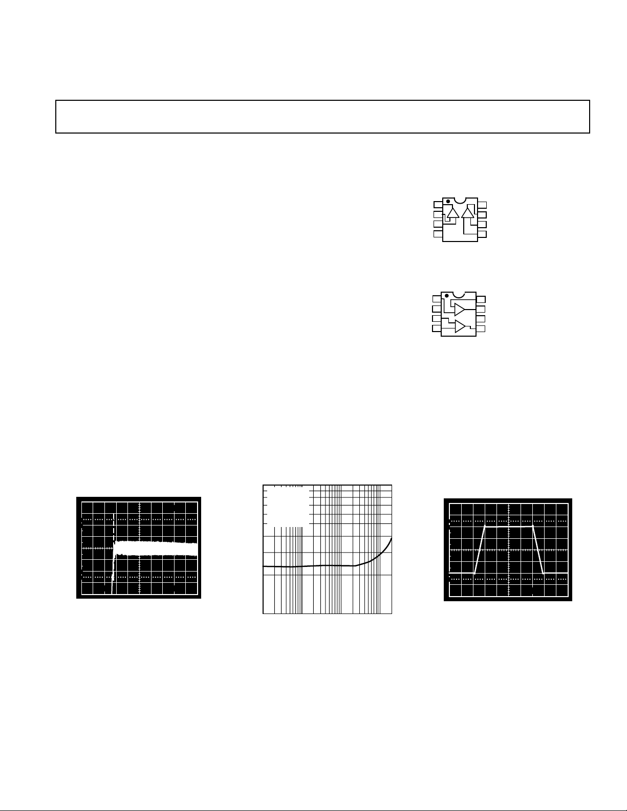
0.010
TA = 25ⴗC
= ⴞ15V
V
S
= 10V p-p
870ns
100
90
10
0%
10mV
500ns
Figure 1. Fast Settling (0.01%)
V
O
= 10k⍀
R
L
= 1
A
V
0.001
20 10k
100 1k 20k
Figure 2. Low Distortion AV = 1,
= 10 k
R
L
Ω
REV. E
Information furnished by Analog Devices is believed to be accurate and
reliable. However, no responsibility is assumed by Analog Devices for its
use, nor for any infringements of patents or other rights of third parties that
may result from its use. No license is granted by implication or otherwise
under any patent or patent rights of Analog Devices.
100
90
10
0%
1µs5V
Figure 3. Excellent Output Drive,
= 600
R
L
One Technology Way, P.O. Box 9106, Norwood, MA 02062-9106, U.S.A.
Tel: 781/329-4700 www.analog.com
Fax: 781/326-8703 © Analog Devices, Inc., 2002
Ω
Page 2

OP249–SPECIFICATIONS
ELECTRICAL CHARACTERISTICS
(@ VS = ⴞ15 V, TA = 25ⴗC, unless otherwise noted.)
OP249A OP249F
Parameter Symbol Conditions Min Typ Max Min Typ Max Unit
Offset Voltage V
Long Term Offset Voltage V
OS
OS
(Note 1) 0.8 1.0 mV
0.2 0.5 0.2 0.7 mV
Offset Stability 1.5 1.5 µV/Month
Input Bias Current I
Input Offset Current I
B
OS
VCM = 0 V, TJ = 25°C 30 75 3075pA
VCM = 0 V, TJ = 25°C625 625pA
Input Voltage Range IVR (Note 2) 12.5 12.5 V
±11 ±11 V
–12.5 –12.5 V
Common-Mode Rejection CMR V
Power-Supply Rejection Ratio PSRR V
Large-Signal Voltage Gain A
Output Voltage Swing V
VO
O
= ±11 V 80 90 80 90 dB
CM
= ±4.5 V to ±18 V 12 31.6 12 50 µV/V
S
VO = ±10 V, RL = 2 kΩ 1000 1400 500 1200 V/mV
RL = 2 kΩ 12.5 12.5 V
±12.0 ±12.0 V
–12.5 –12.5 V
Short-Circuit Current Limit I
SC
Output Shorted to 36 36 mA
Ground ±20 ±50 ±20 ± 50 mA
–33 –33 mA
Supply Current I
SY
Slew Rate SR R
Gain-Bandwidth Product GBW (Note 3) 3.5 4.7 3.5 4.7 MHz
Settling Time t
Phase Margin θ
Differential Input Impedance Z
Open-Loop Output Resistance R
Voltage Noise e
Voltage Noise Density e
Current Noise Density i
Voltage Supply Range V
NOTES
1
Long-term offset voltage is guaranteed by a 1000 HR life test performed on three independent wafer lots at 125 °C with LTPD of three.
2
Guaranteed by CMR test.
3
Guaranteed by design.
4
Settling time is sample tested.
Specifications subject to change without notice.
S
0
IN
O
p-p 0.1 Hz to 10 Hz 2 2 µV p-p
n
n
n
S
No Load, VO = 0 V 5.6 7.0 5.6 7.0 mA
= 2 kΩ, CL = 50 pF 18 22 18 22 V/µs
L
10 V Step 0.01%
0 dB Gain 55 55 Degrees
4
0.9 1.2 0.9 1.2 µs
1012610
12
6 ΩpF
35 35 Ω
fO = 10 Hz 75 75 nV/√Hz
= 100 Hz 26 26 nV/√Hz
f
O
= 1 kHz 17 17 nV/√Hz
f
O
= 10 kHz 16 16 nV/√Hz
f
O
fO = 1 kHz 0.003 0.003 pA/√Hz
±4.5 ±15 ±18 ±4.5 ± 15 ± 18 V
ELECTRICAL CHARACTERISTICS
(@ VS = ⴞ15 V, TA = 25ⴗC, unless otherwise noted.)
OP249G
Parameter Symbol Conditions Min Typ Max Unit
Offset Voltage V
Input Bias Current I
Input Offset Current I
B
OS
OS
VCM = 0 V, TJ = 25°C4075pA
VCM = 0 V, TJ = 25°C1025pA
0.4 2.0 mV
Input Voltage Range IVR (Note 1) 12.5 V
±11 V
–12.0 V
Common-Mode Rejection CMR V
Power Supply Rejection Ratio PSRR V
Large Signal Voltage Gain A
Output Voltage Swing V
VO
O
= ±11 V 76 90 dB
CM
= ±4.5 V to ±18 V 12 50 µV/V
S
VO = ±10 V; RL = 2 kΩ 500 1100 V/mV
RL = 2 kΩ 12.5 V
±12.0 V
–12.5 V
Short-Circuit Current Limit I
SC
Output Shorted to Ground 36 mA
±20 ±50 mA
–33 mA
Supply Current I
SY
Slew Rate SR R
No Load; VO = 0 V 5.6 7.0 mA
= 2 kΩ, CL = 50 pF 18 22 V/µs
L
Gain Bandwidth Product GBW (Note 2) 4.7 MHz
Settling Time t
Phase Margin θ
Differential Input Impedance Z
S
0
IN
10 V Step 0.01% 0.9 1.2 µs
0 dB Gain 55 Degree
10126 ΩpF
–2–
REV. E
Page 3

OP249
OP249G
Parameter Symbol Conditions Min Typ Max Unit
Open Loop Output Resistance R
Voltage Noise e
Voltage Noise Density e
Current Noise Density i
Voltage Supply Range V
NOTES
1
Guaranteed by CMR test.
2
Guaranteed by design.
Specifications subject to change without notice.
O
p-p 0.1 Hz to 10 Hz 2 µV p-p
n
n
n
S
ELECTRICAL CHARACTERISTICS
fO = 10 Hz 75 nV/√Hz
= 100 Hz 26 nV/√Hz
f
O
= 1 kHz 17 nV/√Hz
f
O
= 10 kHz 16 nV/√Hz
f
O
fO = 1 kHz 0.003 pA/√Hz
±4.5 ± 15 ±18 V
(@ VS = ⴞ15 V, –40ⴗC ≤ TA ≤ +85ⴗC for F grades and –55ⴗC ≤ TA ≤ +125ⴗC for A grade
unless otherwise noted.)
35 Ω
Parameter Symbol Conditions Min Typ Max Min Typ Max Unit
OP249A OP249F
Offset Voltage V
OS
0.12 1.0 0.5 1.1 mV
Offset Voltage Temperature
Coefficient TCV
Input Bias Current I
Input Offset Current I
B
OS
OS
(Note 1) 4 20 0.3 4.0 nA
(Note 1) 0.04 4 0.02 1.2 nA
1 5 2.2 6 µV/°C
Input Voltage Range IVR (Note 2) 12.5 12.5 V
±11 ±11 V
–12.5 –12.5 V
Common-Mode Rejection CMR V
Power-Supply Rejection Ratio PSRR V
Large-Signal Voltage Gain A
Output Voltage Swing V
VO
O
= ±11 V 76 110 80 90 dB
CM
= ±4.5 V to ±18 V 5 50 7 100 µV/V
S
RL = 2 kΩ; VO = ±10 V 500 1400 250 1200 V/mV
RL = 2 kΩ 12.5 12.5 V
±12 ±12 V
–12.5 –12.5 V
Short-Circuit Current Limit I
SC
Output Shorted to
Ground ± 10 ± 60 ± 18 ±60 mA
Supply Current I
NOTES
1
TJ = 85°C for F Grades; TJ = 125°C for A Grade.
2
Guaranteed by CMR test.
Specifications subject to change without notice.
SY
ELECTRICAL CHARACTERISTICS
No Load, VO = 0 V 5.6 7.0 5.6 7.0 mA
(@ VS = ⴞ15 V, –40ⴗC ≤ TA ≤ +85ⴗC for unless otherwise noted.)
OP249G
Parameter Symbol Conditions Min Typ Max Unit
Offset Voltage V
OS
1.0 3.6 mV
Offset Voltage Temperature
Coefficient TCV
Input Bias Current I
Input Offset Current I
B
OS
OS
(Note 1) 0.5 4.5 nA
(Note 1) 0.04 1.5 nA
625 µV/°C
Input Voltage Range IVR (Note 2) 12.5 V
±11 V
–12.5 V
Common-Mode Rejection CMR V
Power-Supply Rejection Ratio PSRR V
Large-Signal Voltage Gain A
Output Voltage Swing V
VO
O
= ±11 V 76 95 dB
CM
= ±4.5 V to ±18 V 10 100 µV/V
S
RL = 2 kΩ; VO = ±10 V 250 1200 V/mV
RL = 2 kΩ 12.5 V
±12.0 V
–12.5 V
Short-Circuit Current Limit I
Supply Current I
NOTES
1
TJ = 85°C.
2
Guaranteed by CMR test.
Specifications subject to change without notice.
SC
SY
Output Shorted to Ground ±18 ±60 mA
No Load, VO = 0 V 5.6 7.0 mA
–3–REV. E
Page 4
OP249
WARNING!
ESD SENSITIVE DEVICE
ABSOLUTE MAXIMUM RATINGS
Supply Voltage . . . . . . . . . . . . . . . . . . . . . . . . . . . . . . . ±18 V
Input Voltage
Differential Input Voltage
2
. . . . . . . . . . . . . . . . . . . . . . . . . . . . . . ±18 V
2
. . . . . . . . . . . . . . . . . . . . . . . 36 V
1
Output Short-Circuit Duration . . . . . . . . . . . . . . . . Indefinite
Storage Temperature Range . . . . . . . . . . . . –65°C to +175°C
Operating Temperature Range
OP249A (Z) . . . . . . . . . . . . . . . . . . . . . . . –55°C to +125°C
OP249E, F (Z) . . . . . . . . . . . . . . . . . . . . . –40°C to +85°C
OP249G (P, S) . . . . . . . . . . . . . . . . . . . . . –40°C to +85°C
Junction Temperature
OP249 (Z) . . . . . . . . . . . . . . . . . . . . . . . . –65°C to +175°C
OP249 (P, S) . . . . . . . . . . . . . . . . . . . . . . –65°C to +150°C
Lead Temperature Range (Soldering, 60 sec) . . . . . . . 300°C
ORDERING GUIDE
Model Temperature Range Package Descriptions Package Options
OP249AZ –55°C to +125°C 8-Lead Cerdip Q-8
OP249FZ –40°C to +85°C 8-Lead Cerdip Q-8
OP249GP –40°C to +85°C 8-Lead Plastic DIP N-8
OP249GS
*
–40°C to +85°C 8-Lead SO SO-8
OP249GS-REEL –40°C to +85°C 8-Lead SO SO-8
OP249GS-REEL7 –40°C to +85°C 8-Lead SO SO-8
NOTES
*For availability and burn-in information on SO and PLCC packages, contact your local sales office.
Package Type
3
JA
JC
Unit
8-Lead Hermetic DIP (Z) 134 12 °C/W
8-Lead Plastic DIP (P) 96 37 °C/W
8-Lead SO (S) 150 41 °C/W
NOTES
1
Absolute maximum ratings apply to packaged parts, unless otherwise noted.
2
For supply voltages less than ± 18 V, the absolute maximum input voltage is equal
to the supply voltage.
3
θJA is specified for worst-case mounting conditions, i.e., θJA is specified for device
in socket for cerdip and P-DIP packages; θJA is specified for device soldered to
printed circuit board for SO package.
*
For Military processed devices, please refer to the Standard Microcircuit Drawing (SMD) available at
www.dscc.dla.mil/programs/milspec/default.asp
SMD Part Number ADI Equivalent
5962-9151901M2A OP249ARCMDA
5962-9151901MGA OP249AJMDA
5962-9151901MPA OP249AZMDA
CAUTION
ESD (electrostatic discharge) sensitive device. Electrostatic charges as high as 4000 V readily
accumulate on the human body and test equipment and can discharge without detection. Although
the OP249 features proprietary ESD protection circuitry, permanent damage may occur on
devices subjected to high-energy electrostatic discharges. Therefore, proper ESD precautions are
recommended to avoid performance degradation or loss of functionality.
–4–
REV. E
Page 5
Typical Performance Characteristics–
OP249
120
TA = 25ⴗC
100
OPEN-LOOP GAIN – dB
–20
= ⴞ15V
V
S
= 2k⍀
R
L
80
60
40
20
0
1k
GAIN
PHASE
10k 100k 1M 10M 100M
FREQUENCY – Hz
⍜m = 55
TPC 1. Open-Loop Gain, Phase vs.
Frequency
120
TA = 25ⴗC
= ⴞ15V
V
S
+PSRR
–PSRR
10k 100k 1M
POWER SUPPLY REJECTION – dB
100
80
60
40
20
0
10
100
FREQUENCY – Hz
1k
TPC 4. Power Supply Rejection vs.
Frequency
0
45
90
135
180
225
65
VS = ⴞ15V
60
⍜m
55
PHASE – ⴗC
PHASE MARGIN – ⴗC
50
45
–75
–50 –25 0 25 50 75 100 125
TEMPERATURE – ⴗC
GBW
TPC 2. Gain Bandwidth Product,
Phase Margin vs. Temperature
28
VS = ⴞ15V
= 2k⍀
R
L
26
CL = 50pF
24
22
20
SLEW RATE – V/s
18
16
–50 –25 0 25 50 75 100 125
–75
TEMPERATURE – ⴗC
–SR
+SR
TPC 5. Slew Rate vs. Temperature
10
8
6
4
2
GAIN BANDWIDTH PRODUCT – MHz
COMMON-MODE REJECTION – dB
140
120
100
TA = 25ⴗC
= ⴞ15V
V
S
80
60
40
20
0
100
1k
10k 100k 1M 10M
FREQUENCY – Hz
TPC 3. Common-Mode Rejection vs.
Frequency
28
TA = 25ⴗC
= ⴞ15V
V
S
26
= 2k⍀
R
L
24
22
20
SLEW RATE – V/s
18
16
0.2 0.4 0.6 0.8 1.0
0
DIFFERENTIAL INPUT VOLTAGE – Volts
TPC 6. Slew Rate vs. Differential
Input Voltage
35
TA = 25ⴗC
= ⴞ15V
V
S
30
NEGATIVE
25
20
POSITIVE
15
SLEW RATE – V/s
10
5
100 200 300 400 500
0
CAPACITIVE LOAD – pF
TPC 7. Slew Rate vs. Capacitive
Load
10
TA = 25ⴗC
8
= ⴞ15V
V
–2
–4
OUTPUT STEP SIZE – Volts
–6
–8
–10
S
= 1
A
VCL
6
4
2
0
0
200 400 600 800 1000
0.1%
0.01%
0.01%
0.1%
SETTLING TIME – ns
TPC 8. Settling Time vs. Step Size
–5–REV. E
100
TA = 25ⴗC
= ⴞ15V
V
S
80
60
40
20
VOLTAGE NOISE DENSITY – nV Hz
0
0 100
FREQUENCY – Hz
1k 10k
TPC 9. Voltage Noise Density vs.
Frequency
Page 6

OP249
FREQUENCY – Hz
IMPEDANCE – ⍀
1k
10
0
10k 100k 1M 10M
TA = 25ⴗC
V
S
= ⴞ15V
50
40
30
20
A
VCL
= 100
A
VCL
= 1
A
VCL
= 10
100
0.010
0.001
20 100
TA = 25ⴗC
= ⴞ15V
V
S
= 10V p-p
V
O
= 10k⍀
R
L
= 1
A
V
1k 10k 20k
TPC 10. Distortion vs. Frequency
0.10
TA = 25ⴗC
= ⴞ15V
V
S
= 10V p-p
V
O
= 10k⍀
R
L
= 1
A
V
0.010
0.001
20 100
TA = 25ⴗC
= ⴞ15V
V
S
= 10V p-p
V
O
= 2k⍀
R
L
= 1
A
V
1k 10k 20k
TPC 11. Distortion vs. Frequency
0.10
TA = 25ⴗC
= ⴞ15V
V
S
= 10V p-p
V
O
= 2k⍀
R
L
= 10
A
V
0.010
0.001
20 100
TA = 25ⴗC
= ⴞ15V
V
S
= 10V p-p
V
O
= 600⍀
R
L
= 1
A
V
1k 10k 20k
TPC 12. Distortion vs. Frequency
0.10
TA = 25ⴗC
= ⴞ15V
V
S
= 10V p-p
V
O
= 600⍀
R
L
= 10
A
V
0.010
20 100
1k 10k 20k
TPC 13. Distortion vs. Frequency
500mV 1s
BANDWIDTH (0.1Hz TO 10Hz)
T
= 25ⴗCVS = ⴞ15V
A
TPC 16. Low Frequency Noise
+1V
–1V
0.010
20 100
1k 10k 20k
TPC 14. Distortion vs. Frequency
CLOSED-LOOP GAIN – dB
–10
–20
60
50
A
= 100
VCL
40
30
A
= 10
VCL
20
A
= 5
VCL
10
0
A
= 1
VCL
1k
10k 100k 1M 10M
FREQUENCY – Hz
TA = 25ⴗC
V
= ⴞ15V
S
TPC 17. Closed-Loop Gain vs.
Frequency
100M
0.010
20 100
1k 10k 20k
TPC 15. Distortion vs. Frequency
TPC 18. Closed-Loop Output
Impedance vs. Frequency
–6–
REV. E
Page 7

OP249
30
25
20
15
10
OUTPUT VOLTAGE – V p-p
5
0
1k
FREQUENCY – Hz
AD8512
OP249
AD712
1M
TPC 19. Output Voltage vs.
Frequency
20
TA = 25ⴗC
15
= 2k⍀
R
L
10
5
0
–5
–10
OUTPUT VOLTAGE SWING – Volts
–15
–20
0
ⴞ5 ⴞ10 ⴞ15 ⴞ20
SUPPLY VOLTAGE – Volts
TPC 22. Output Voltage Swing vs.
Supply Voltage
10M
90
VS = ⴞ15V
80
R
= 2k⍀
L
V
= 100mV p-p
IN
70
A
60
50
40
30
OVERSHOOT – %
20
10
= 1
VCL
NEGATIVE EDGE
A
= 1
VCL
POSITIVE EDGE
A
= 5
0
100
0 200 300 400 500
LOAD CAPACITANCE – pF
VCL
TPC 20. Small Overshoot vs. Load
Capacitance
6.0
VS = ⴞ15V
NO LOAD
5.8
5.6
5.4
SUPPLY CURRENT – mA
5.2
–75
–50 –25 0 25 50 75 100 125
TEMPERATURE – ⴗC
TPC 23. Supply Current vs.
Temperature
16
TA = 25ⴗC
14
= ⴞ15V
V
S
12
10
8
6
4
MAXIMUM OUTPUT SWING – Volts
2
0
100 10k
+V
= |–V
OHM
OHM
LOAD RESISTANCE – ⍀
1k
|
TPC 21. Maximum Output Voltage
vs. Load Resistance
6.0
5.8
TA = 25ⴗC
5.6
TA = 125ⴗC
5.4
SUPPLY CURRENT – mA
TA = –55ⴗC
5.2
5.0
0 5 10 15 20
SUPPLY VOLTAGE – Volts
TPC 24. Supply Current vs. Supply
Voltage
180
TA = 25ⴗC
160
= ⴞ15V
V
S
415 ⴛ OP249
140
(830 OP AMPS)
120
100
80
UNITS
60
40
20
0
–1k
–800
–600
–400
–200
VOS – V
2000600
TPC 25. VOS Distribution
(P Package)
400 800
300
270
240
210
180
150
UNITS
120
90
m
60
30
1k
0
0
4 6 8 10 12 14 16 18 20 22 24
2
VS = ⴞ15V
–40ⴗC TO +85ⴗC
(830 OP AMPS)
V/ⴗC
TPC 26. TCVOS Distribution
(P Package)
50
40
30
20
OFFSET VOLTAGE – V
10
0
0
1
TIME AFTER POWER APPLIED – Minutes
VS = ⴞ15V
24
35
TPC 27. Offset Voltage Warm-Up
Drift
–7–REV. E
Page 8

OP249
10k
VS = ⴞ15V
VCM = 0V
1k
100
10
INPUT BIAS CURRENT – pA
1
–50 –25 0 25 50 75 100 125
–75
TEMPERATURE – ⴗC
TPC 28. Input Bias Current vs.
Temperature
80
TA = 25ⴗC
= 0V
V
CM
60
40
20
INPUT OFFSET CURRENT – pA
0
–75
–50 –25 0 25 50 75 100 125
TEMPERATURE – ⴗC
TPC 31. Input Offset Current vs.
Temperature
4
10
TA = 25ⴗC
= ⴞ15V
V
S
3
10
2
10
BIAS CURRENT – pA
1
10
0
10
–15
–10 –5051015
COMMON-MODE VOLTAGE – Volts
TPC 29. Bias Current vs.
Common-Mode Voltage
80
VS = ⴞ15V
60
40
20
OPEN-LOOP GAIN – V/mV
0
–75
–50 –25 0 25 50 75 100 125
RL = 10k⍀
RL = 2k⍀
TEMPERATURE – ⴗC
TPC 32. Open-Loop Gain vs.
Temperature
50
TA = 25ⴗC
= ⴞ15V
V
S
40
30
20
INPUT BIAS CURRENT – pA
10
0
20
48
TIME AFTER POWER APPLIED – Minutes
610
TPC 30. Bias Current Warm-Up Drift
80
VS = ⴞ15V
60
SOURCE
40
SINK
20
SHORT-CIRCUIT OUTPUT CURRENT – mA
0
–75
–50 –25 0 25 50 75 100 125
TEMPERATURE – ⴗC
TPC 33. Short-Circuit Output Current vs. Junction Temperature
–8–
REV. E
Page 9

OP249
+IN
–IN
Figure 4. Simplified Schematic (1/2 OP249)
1/2
3V
OP249
5k⍀
V+
APPLICATIONS INFORMATION
The OP249 represents a reliable JFET amplifier design, featuring an excellent combination of dc precision and high speed. A
rugged output stage provides the ability to drive a 600 Ω load
V
OUT
and still maintain a clean ac response. The OP249 features a large
signal response that is more linear and symmetric than previously available JFET input amplifiers—compare the OP249’s
large-signal response, as illustrated in Figure 6, to other industry standard dual JFET amplifiers.
Typically, JFET amplifier’s stewing performance is simply specified
as just a number of volts/µs. There is no discussion on the quality,
i.e., linearity, symmetry, etc., of the stewing response.
V–
+18V
1/2
3V
OP249
–18V
Figure 5. Burn-In Circuit
A) OP249
5k⍀
B) LT1057
C) AD712
Figure 6. Large-Signal Transient Response, AV = 1,
= 20 V p-p, ZL = 2 kΩ//200 pF, VS = ±15 V
V
IN
–9–REV. E
Page 10

OP249
The OP249 was carefully designed to provide symmetrically
matched slew characteristics in both the negative and positive
directions, even when driving a large output load.
An amplifier’s slewing limitation determines the maximum
frequency at which a sinusoidal output can be obtained without
significant distortion. It is, however, important to note that the
nonsymmetric stewing typical of previously available JFET
amplifiers adds a higher series of harmonic energy content to
the resulting response—and an additional dc output component.
Examples of potential problems of nonsymmetric slewing
behavior could be in audio amplifier applications, where a natural
low distortion sound quality is desired, and in servo or signal
processing systems where a net dc offset cannot be tolerated.
The linear and symmetric stewing feature of the OP249 makes
it an ideal choice for applications that will exceed the full-power
bandwidth range of the amplifier.
VERTICAL 50V/DIV
INPUT VARIATION
HORIZONTAL 5V/DIV
OUTPUT CHARGE
Figure 8. Open-Loop Gain Linearity. Variation in OpenLoop Gain Results in Errors in High Closed-Loop Gain
Circuits. RL = 600 Ω, VS = ±15 V
R4
50k⍀
+V
V
R5
–V
IN
R1
200k⍀
R3
R2
31⍀
1/2
OP249
V
ADJUST RANGE = ⴞV
OS
V
OUT
R2
R1
Figure 9. Offset Adjust for Inverting Amplifier
Configuration
Figure 7. Small-Signal Transient Response, AV = 1,
= 2 kΩ100 pF, No Compensation, VS = ±15 V
Z
L
As with most JFET-input amplifiers, the output of the OP249
may undergo phase inversion if either input exceeds the specified input voltage range. Phase inversion will not damage the
amplifier, nor will it cause an internal latch-up condition.
Supply decoupling should be used to overcome inductance and
resistance associated with supply lines to the amplifier. A 0.1 µF
and a 10 µF capacitor should be placed between each supply
pin and ground.
OPEN-LOOP GAIN LINEARITY
The OP249 has both an extremely high open-loop gain of
1 kV/mV minimum and constant gain linearity. This feature of
the OP249 enhances its dc precision, and provides superb accuracy in high closed-loop gain applications. Figure 8 illustrates
the typical open-loop gain linearity—high gain accuracy is assured,
even when driving a 600 Ω load.
OFFSET VOLTAGE ADJUSTMENT
The inherent low offset voltage of the OP249 will make offset
adjustments unnecessary in most applications. However, where
a lower offset error is required, balancing can be performed with
simple external circuitry, as illustrated in Figures 9 and 10.
50k⍀
V
+V
R1
R3
200k⍀
–V
IN
33⍀
R4
R2
R5
1/2
OP249
V
ADJUST RANGE = ⴞV
OS
V
OUT
GAIN = = 1 +
V
IN
R5
1 +
IF R2 << R4
R4
R5
R4 + R2
V
OUT
R2
R1
Figure 10. Offset Adjust for Noninverting Amplifier
Configuration
In Figure 9, the offset adjustment is made by supplying a small
voltage at the noninverting input of the amplifier. Resistors R1
and R2 attenuates the pot voltage, providing a ±2.5 mV (with
= ±15 V) adjustment range, referred to the input. Figure 10
V
S
illustrates offset adjust for the noninverting amplifier configuration, also providing a ±2.5 mV adjustment range. As indicated
in the equations in Figure 10, if R4 is not much greater than R2,
there will be a resulting closed-loop gain error that must be
accounted for.
–10–
REV. E
Page 11

OP249
SETTLING TIME
Settling time is the time between when the input signal begins
to change and when the output permanently enters a prescribed
error band. The error bands on the output are 5 mV and 0.5 mV,
respectively, for 0.1% and 0.01% accuracy.
Figure 11 illustrates the OP249’s typical settling time of 870 ns.
Moreover, problems in settling response, such as thermal tails
and long-term ringing are nonexistent.
870ns
100
90
10
0%
10mV
500ns
Figure 11. Settling Characteristics of the OP249 to 0.01%
DAC OUTPUT AMPLIFIER
Unity-gain stability, a low offset voltage of 300 µV typical, and a
fast settling time of 870 ns to 0.01%, makes the OP249 an ideal
amplifier for fast digital-to-analog converters.
For CMOS DAC applications, the low offset voltage of the
OP249 results in excellent linearity performance. CMOS DACs,
such as the PM-7545, will typically have a code-dependent
output resistance variation between 11 kΩ and 33 kΩ. The
change in output resistance, in conjunction with the 11 kΩ
feedback resistor, will result in a noise gain change. This causes
variations in the offset error, increasing linearity errors. The
OP249 features low offset voltage error, minimizing this effect
and maintaining 12-bit linearity performance over the full-scale
range of the converter.
Since the DAC’s output capacitance appears at the operational
amplifiers inputs, it is essential that the amplifier is adequately
compensated. Compensation will increase the phase margin,
and ensure an optimal overall settling response. The required
lead compensation is achieved with Capacitor C in Figure 12.
REFERENCE
OR V
REFERENCE
OR V
IN
500⍀
IN
V
DB11 – DB
DATA INPUT
500⍀
V
V
REF
V
DD
0.1F
V
DD
V
PM7545
REF
DB11 – DB
DATA INPUT
DGND
0
12
a. Unipolar Operation
DD
DD
12
0.1F
PM7545
0
R
AGND
DGND
FB
OUT
75⍀
1
b. Bipolar Operation
R
FB
AGND
OUT
75⍀
1
C
33pF
20k⍀
+15V
1/2
OP249
R4
1%
C
33pF
0.1F
+15V
1/2
OP249
–15V
R3
10k⍀
1%
0.1F
0.1F
10k⍀
1/2
OP249
–15V
R5
1%
V
OUT
0.1F
V
OUT
Figure 12. Fast Settling and Low Offset Error of the OP249 Enhances CMOS DAC Performance
–11–REV. E
Page 12

OP249
BA
RESPONSE IS GROSSLY UNDERDAMPED,
C = 5pF
AND EXHIBITS RINGING
FAST RISE TIME CHARACTERISTICS, BUT AT EXPENSE
OF SLIGHT PEAKING IN RESPONSE
C = 15pF
Figure 13. Effect of Altering Compensation from Circuit in Figure 12a—PM7545 CMOS DAC with 1/2 OP249, Unipolar
Operation. Critically Damped Response Will Be Obtained with C
Figure 13 illustrates the effect of altering the compensation on
33 pF.
+15V
0.1F
the output response of the circuit in Figure 12a. Compensation
is required to address the combined effect of the DAC’s output
capacitance, the op amp’s input capacitance and any stray capacitance. Slight adjustments to the compensation capacitor may be
required to optimize settling response for any given application.
The settling time of the combination of the current output DAC
and the op amp can be approximated by:
tSTOTAL = (tSDAC )2+(tSAMP )
2
The actual overall settling time is affected by the noise gain of
the amplifier, the applied compensation, and the equivalent
input capacitance at the amplifier’s input.
DISCUSSION ON DRIVING A/D CONVERTERS
Settling characteristics of operational amplifiers also include an
amplifier’s ability to recover, i.e., settle, from a transient current
output load condition. An example of this includes an op amp
driving the input from a SAR type A/D converter. Although the
comparison point of the converter is usually diode clamped, the
input swing of plus-and-minus a diode drop still gives rise to a
significant modulation of input current. If the closed-loop output
impedance is low enough and bandwidth of the amplifier is
sufficiently large, the output will settle before the converter
makes a comparison decision which will prevent linearity errors
or missing codes.
Figure 14 shows a settling measurement circuit for evaluating
recovery from an output current transient. An output disturbing
current generator provides the transient change in output
load current of 1 mA. As seen in Figure 15, the OP249 has
extremely fast recovery of 274 ns (to 0.01%), for a 1 mA load
transient. The performance makes it an ideal amplifier for
1/2
OP249
0.1F
2N2907
220⍀
*
*
1k⍀
0.01F
1k⍀
2N3904
10F
0.47F
V
REF
–15V
300pF
+15V
1.5k⍀
TTL INPUT
*NOTE: DECOUPLE CLOSE TOGETHER
1N4148
+15V
1.8k⍀
0.1F
ON GROUND PLANE WITH
SHORT LEAD LENGTHS
Figure 14. Transient Output Impedance Test Fixture
The combination of high speed and excellent dc performance of
the OP249 makes it an ideal amplifier for 12-bit data acquisition
systems. Examining the circuit in Figure 16, one amplifier in the
OP249 provides a stable –5 V reference voltage for the V
of the ADC912. The other amplifier in the OP249 performs
high speed buffering of the A/D’s input.
Examining the worst case transient voltage error (Figure 17) at
the Analog In node of the A/D converter: the OP249 recovers in
less than 100 ns. The fast recovery is due to both the OP249’s
wide bandwidth and low dc output impedance.
⌬I
OUT
7A13 PLUG-IN
7A13 PLUG-IN
|V
|
REF
=
1k⍀
input
REF
data acquisition systems.
–12–
REV. E
Page 13

OP249
Figure 15. OP249’s Transient Recovery Time from a 1 mA
Load Transient to 0.01%
+5V –15V
ANALOG IN
V
REF
AGND
–5V
10F||0.1F
ADC912
IN
DGND HBEN
10F||0.1F10F||0.1F
RD
CLK IN
BUSY
CS
ANALOG
INPUT
+15V
0.1F
IN
REF02
OUT
GND
+15V
1/2
OP249
–15V
0.1F
1/2
OP249
0.1F
0.1F
10⍀
Figure 16. OP249 Dual Amplifiers Provide Both Stable –5 V
Reference Input, and Buffers Input to ADC912
Figure 17. Worst-Case Transient Voltage, at Analog In,
Occurs at the Half-Scale Point of the A/D. OP249 Buffers
the A/D Input from Figure 16, and Recovers in Less than
100 ns.
–13–REV. E
Page 14

OP249
OP249 SPICE MACRO-MODEL
Figures 18 and Table I show the node and net list for a SPICE
macromodel of the OP249 The model is a simplified version of
the actual device and simulates important dc parameters such as
, IOS, IB, AVO, CMR, VO and ISY. AC parameters such as slew
V
OS
rate, gain and phase response and CMR change with frequency
are also simulated by the model.
99
V2
8
10
G1
D1
9
D2
G2
V3
IN–
IN+
I1
4
2
I
OS
1
C
IN
99
R1
R2
3
J1 J2
5
R3 R4
50
E
OS
C2
7
6
The model uses typical parameters for the OP249. The poles
and zeros in the model were determined from the actual open
and closed-loop gain and phase response of the OP249. In this
way, the model presents an accurate ac representation of the actual
device. The model assumes an ambient temperature of 25°C.
C5
12
R5
C3
R6
C4
G3
G4
R7
R9
14
R10
R8
13
C6
G5
G6
R11
L1
15
R12
R13
16
L2
R14
L3
21
G19
G20
G13
G14
R27
R28
R21
R22
22
L5
L4
30
V
OUT
R15
R16
R23
R24
C9
C10
C15
C16
G7
17
G8
50
99
G15
23
G16
G9
R17
C11
18 19 20
G10
R18
C12
R25
D3
25
24
D4
26
R26
D7 D8
G11
G12
D5 D6
27 28
G17 G18
R19
R20
C13
C14
V4
+ –
29
V5
+ –
50
Figure 18. Macro-Model
–14–
REV. E
Page 15

Table I. SPICE Net List
OP249 MACRO-MODEL
• subckt OP249 1 2 30 99 50
*
INPUT STAGE & POLE AT 100MHz
*
r1 2 3 5E11
r2 1 3 5E11
r3 5 50 652.3
r4 6 50 652.3
cin 1 2 5E-12
c2 5 6 1.22E-12
i1 99 4 1E-3
ios 1 2 3.1E-12
eos 7 1 poly(1) 20 24 150E-6 1
j1 5 2 4 jx
j2 6 7 4 jx
*
* SECOND STAGE & POLE AT 12.2Hz
*
r5 9 99 326.1E6
r6 9 50 326.1E6
c3 9 99 40E-12
c4 9 50 40E-12
g1 99 9 poly(1) 5 6 4.25E-3 1.533E-3
g2 9 50 poly(1) 6 5 4.25E-3 1.533E-3
v2 99 8 2.9
v3 10 50 2.9
d1 9 8 dx
d2 10 9 dx
*
* POLE-ZERO PAIR AT 2MHz/4.0MHz
*
r7 11 99 1E6
r8 11 50 1E6
r9 11 12 1E6
r10 11 13 1E6
c5 12 99 37.79E-15
c6 13 50 37.79E-15
g3 99 11 9 24 1E-6
g4 11 50 24 9 1E-6
*
* ZERO-POLE PAIR AT 4MHz/8MHz
*
r11 99 15 IE6
r12 14 15 1E6
r13 14 16 1E6
r14 50 16 1E6
I1 99 15 19.89E-3
I2 50 16 19.89E-3
g5 99 14 11 24 1E-6
g6 14 50 24 11 1E-6
*
* POLE AT 20MHz
*
r15 17 99 1E6
r16 17 50 1E6
c9 17 99 7.96E-15
c10 17 50 7.96E-15
g7 99 17 14 24 1E-6
g8 17 50 24 14 1E-6
*
* POLE AT 50MHz
*
r17 18 99 1E6
r18 18 50 1E6
c11 18 99 3.18E-15
c12 18 50 3.18E-15
g9 99 18 17 24 1E-6
g10 18 50 24 17 1E-6
OP249
*
* POLE AT 50MHz
*
r19 19 99 1E6
r20 19 50 1E6
c13 19 99 3.18E-15
c14 19 50 3.18E-15
g11 99 19 18 24 1E-6
g12 19 50 24 18 1E-6
*
* COMMON-MODE GAIN NETWORK WITH ZERO AT 60kHZ
*
r21 20 21 1E6
r22 20 22 1E6
I3 21 99 2.65
I4 22 50 2.65
g13 99 20 3 24 1.78E-11
g14 20 50 24 3 1.78E-11
*
* POLE AT 50MHZ
*
r23 23 99 1E6
r24 23 50 1E6
c15 23 99 3.18E-15
c16 23 50 3.18E-15
g15 99 23 19 24 1E-6
g16 23 50 24 19 1E-6
*
* OUTPUT STAGE
*
r25 24 99 135E3
r26 24 50 135E3
r27 29 99 70
r28 29 50 70
I5 29 30 4E-7
g17 27 50 23 29 14.3E-3
g18 28 50 29 23 14.3E-3
g19 29 99 99 23 14.3E-3
g20 50 29 23 50 14.3E-3
v4 25 29 .4
v5 29 26 .4
d3 23 25 dx
d4 26 23 dx
d5 99 27 dx
d6 99 28 dx
d7 50 27 dy
d8 50 28 dy
*
MODELS USED
*
• model jx PJF(BETA=1.175E-3 VTO=–2.000 IS=21E-12)
• model dx D(IS=1E-15)
• model dy D(IS=1E-15 BV=50)
• ends OP249
** PSpice is a registered trademark of MicroSim Corporation.
**
HSPICE is a tradename of Meta-Software, Inc.
–15–REV. E
Page 16

OP249
OUTLINE DIMENSIONS
Dimensions shown in inches and (mm).
0.210 (5.33)
MAX
0.160 (4.06)
0.115 (2.93)
0.022 (0.558)
0.014 (0.356)
8-Lead Plastic DIP
(N-8)
0.430 (10.92)
0.348 (8.84)
8
14
PIN 1
0.100
(2.54)
BSC
5
0.280 (7.11)
0.240 (6.10)
0.060 (1.52)
0.015 (0.38)
0.070 (1.77)
0.045 (1.15)
0.130
(3.30)
MIN
SEATING
PLANE
0.325 (8.25)
0.300 (7.62)
0.015 (0.381)
0.008 (0.204)
0.200 (5.08)
MAX
0.200 (5.08)
0.125 (3.18)
0.023 (0.58)
0.014 (0.36)
0.195 (4.95)
0.115 (2.93)
0.005 (0.13)
MIN
8
1
0.405 (10.29)
8-Lead Cerdip
0.055 (1.4)
MAX
5
4
PIN 1
MAX
0.070 (1.78)
0.100
(2.54)
0.030 (0.76)
BSC
(Q-8)
0.310 (7.87)
0.220 (5.59)
0.060 (1.52)
0.015 (0.38)
0.150
(3.81)
MIN
SEATING
PLANE
0.1574 (4.00)
0.1497 (3.80)
PIN 1
0.0098 (0.25)
0.0040 (0.10)
SEATING
PLANE
0.320 (8.13)
0.290 (7.37)
15ⴗ
0ⴗ
8-Lead Narrow Body (SOIC)
(SO-8)
0.1968 (5.00)
0.1890 (4.80)
8
5
0.2440 (6.20)
41
0.2284 (5.80)
0.0688 (1.75)
0.0532 (1.35)
0.0500
(1.27)
BSC
0.015 (0.38)
0.008 (0.20)
0.0192 (0.49)
0.0138 (0.35)
0.0098 (0.25)
0.0075 (0.19)
8°
0°
0.0196 (0.50)
0.0099 (0.25)
0.0500 (1.27)
0.0160 (0.41)
x 45°
C00296a–0–1/02(E)
Revision History
Location Page
9/01—Data Sheet changed from REV. D to REV. E.
Edits to FEATURES . . . . . . . . . . . . . . . . . . . . . . . . . . . . . . . . . . . . . . . . . . . . . . . . . . . . . . . . . . . . . . . . . . . . . . . . . . . . . . . . . . . . . 1
Edits to PIN CONNECTIONS . . . . . . . . . . . . . . . . . . . . . . . . . . . . . . . . . . . . . . . . . . . . . . . . . . . . . . . . . . . . . . . . . . . . . . . . . . . . . 1
Edits to ELECTRICAL CHARACTERISTICS . . . . . . . . . . . . . . . . . . . . . . . . . . . . . . . . . . . . . . . . . . . . . . . . . . . . . . . . . . . . . . 2, 3
Edits to ABSOLUTE MAXIMUM RATINGS . . . . . . . . . . . . . . . . . . . . . . . . . . . . . . . . . . . . . . . . . . . . . . . . . . . . . . . . . . . . . . . . . 4
Edits to PACKAGE TYPE . . . . . . . . . . . . . . . . . . . . . . . . . . . . . . . . . . . . . . . . . . . . . . . . . . . . . . . . . . . . . . . . . . . . . . . . . . . . . . . . 4
Edits to ORDERING GUIDE . . . . . . . . . . . . . . . . . . . . . . . . . . . . . . . . . . . . . . . . . . . . . . . . . . . . . . . . . . . . . . . . . . . . . . . . . . . . . . 4
Deleted WAFER TEST LIMITS . . . . . . . . . . . . . . . . . . . . . . . . . . . . . . . . . . . . . . . . . . . . . . . . . . . . . . . . . . . . . . . . . . . . . . . . . . . 5
Deleted DICE CHARACTERISTICS . . . . . . . . . . . . . . . . . . . . . . . . . . . . . . . . . . . . . . . . . . . . . . . . . . . . . . . . . . . . . . . . . . . . . . . 5
Edits to TYPICAL PERFORMANCE CHARACTERISTICS . . . . . . . . . . . . . . . . . . . . . . . . . . . . . . . . . . . . . . . . . . . . . . . . . . . . . 8
Edits to Macro-Model Figure . . . . . . . . . . . . . . . . . . . . . . . . . . . . . . . . . . . . . . . . . . . . . . . . . . . . . . . . . . . . . . . . . . . . . . . . . . . . . 15
Edits to OUTLINE DIMENSIONS . . . . . . . . . . . . . . . . . . . . . . . . . . . . . . . . . . . . . . . . . . . . . . . . . . . . . . . . . . . . . . . . . . . . . . . . 17
–16–
PRINTED IN U.S.A.
 Loading...