

Page 1
Dual, Precision
O
0
www.BDTIC.com/ADI
JFET High Speed Operational Amplifier
FEATURES
Fast slew rate: 22 V/s typical
Settling time (0.01%): 1.2 µs maximum
Offset voltage: 300 µV maximum
High open-loop gain: 1000 V/mV minimum
Low total harmonic distortion: 0.002% typical
Improved replacement for AD712, LT1057, OP215, TL072,
and MC34
APPLICATIONS
Output amplifier for fast DACs
Signal processing
Instrumentation amplifiers
Fast sample-and-holds
Active filters
Low distortion audio amplifiers
Input buffer for ADCs
Servo controllers
082
OP249
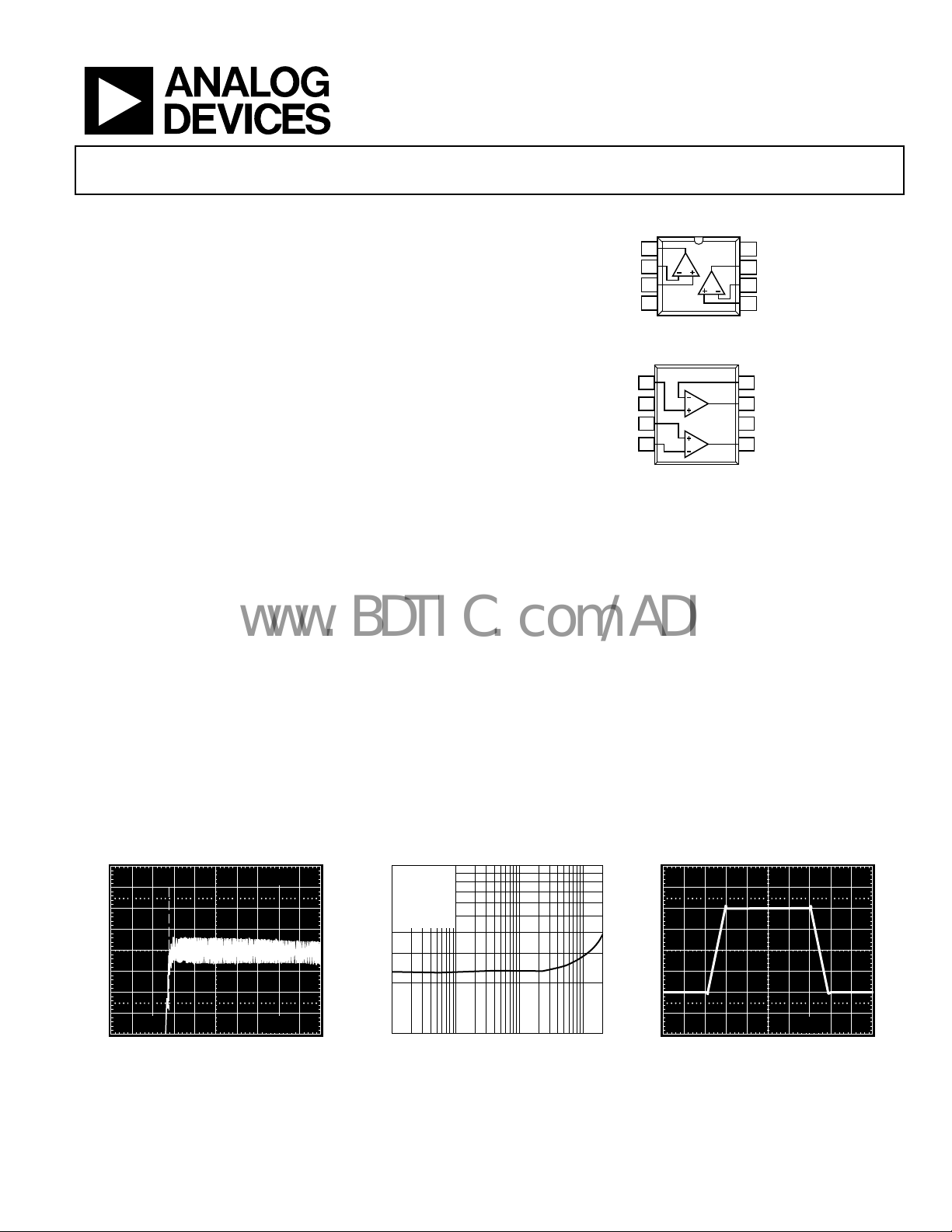
PIN CONFIGURATIONS
UT A
1
OP249
A
2
–IN A
+IN A
3
V–
4
B
Figure 1. 8-Lead CERDIP (Q-8) and
8-Lead
PDIP (N-8)
1
+IN A
+IN B
–IN B
2
V–
3
4
A
OP249
B
Figure 2. 8-Lead SOIC (R-8)
8
7
6
5
8
7
6
5
V+
OUT B
–IN B
+IN B
–IN A
OUT A
V+
OUT B
00296-001
00296-002
GENERAL DESCRIPTION
The OP249 is a high speed, precision dual JFET op amp, similar to
the popular single op amp, the OP42. The OP249 outperforms
available dual amplifiers by providing superior speed with
excellent dc performance. Ultrahigh open-loop gain (1 kV/mV
minimum), low offset voltage, and superb gain linearity makes
the OP249 the industry’s first true precision, dual high speed
amplifier.
With a slew rate of 22 V/μs typical and a fast settling time of less
n 1.2 μs maximum to 0.01%, the OP249 is an ideal choice for
tha
high speed bipolar DAC and ADC applications. The excellent
dc performance of the OP249 allows the full accuracy of high
resolution CMOS DACs to be realized.
0.01
.001
TA = 25°C
= ±15V
V
S
= 10V p-p
V
O
= 10kΩ
R
L
= 1
A
V
20
100 1k 10k 20k
100
870ns
90
10
0%
500ns10mV
00296-003
Figure 3. Fast Settling (0.01%) Figure 4. Low Distortion, A
Symmetrical slew rate, even when driving large load, such as,
600 Ω o
r 200 pF of capacitance and ultralow distortion, make
the OP249 ideal for professional audio applications, active filters,
high speed integrators, servo systems, and buffer amplifiers.
The OP249 provides significant performance upgrades to the
TL072, AD712,
= 1, RL = 10 kΩ Figure 5. Excellent Output Drive, RL = 600 Ω
V
OP215, MC34082, and LT1057.
100
90
10
0%
00296-004
5V 1µs
00296-005
Rev. F
Information furnished by Analog Devices is believed to be accurate and reliable. However, no
responsibility is assumed by Anal og Devices for its use, nor for any infringements of patents or ot her
rights of third parties that may result from its use. Specifications subject to change without notice. No
license is granted by implication or otherwise under any patent or patent rights of Analog Devices.
Trademarks and registered trademarks are the property of their respective owners.
One Technology Way, P.O. Box 9106, Norwood, MA 02062-9106, U.S.A.
Tel: 781.329.4700 www.analog.com
Fax: 781.461.3113 ©2007 Analog Devices, Inc. All rights reserved.
Page 2

OP249
www.BDTIC.com/ADI
TABLE OF CONTENTS
Features .............................................................................................. 1
Applications....................................................................................... 1
Pin Configurations ........................................................................... 1
General Description......................................................................... 1
Revision History ............................................................................... 2
Specifications..................................................................................... 3
Electrical Characteristics............................................................. 3
Absolute Maximum Ratings............................................................ 6
ESD Caution.................................................................................. 6
REVISION HISTORY
5/07—Rev. E to Rev. F
Updated Format..................................................................Universal
Changes to Table 1............................................................................ 3
Changes to Table 2............................................................................ 4
Changes to Table 3 and Table 4....................................................... 5
Changes to Table 5............................................................................ 6
Changes to Figure 31...................................................................... 11
Changes to Figure 37 and Figure 38............................................. 12
Deleted OP249 SPICE Macro-Model Section ............................ 14
Deleted Figure 18; Renumbered Sequentially ............................ 14
Deleted Table I ................................................................................ 15
Changes to Discussion on Driving ADCs Section..................... 17
Updated Outline Dimensions....................................................... 18
Changes to Ordering Guide.......................................................... 19
Typical Perf or m an c e Charac t e r istics ..............................................7
Applications Information.............................................................. 13
Open-Loop Gain Linearity ....................................................... 14
Offset Voltage Adjustment........................................................ 14
Settling Time............................................................................... 14
DAC Output Amplifier.............................................................. 15
Disscusion on Driving ADCs ................................................... 16
Outline Dimensions ....................................................................... 18
Ordering Guide .......................................................................... 19
9/01—Rev. D to Rev. E
E
dits to Features and Pin Connections ..........................................1
Edits to Electrical Characteristics .............................................. 2, 3
Edits to Absolute Maximum Ratings, Package Type, and
Ordering Guide..................................................................................4
Deleted Wafer Test Limits and Dice Characteristics Section ......5
Edits to Typical Performance Characteristics................................8
Edits to Macro-Model Figure........................................................ 15
Edits to Outline Dimensions......................................................... 17
Rev. F | Page 2 of 20
Page 3
OP249
www.BDTIC.com/ADI
SPECIFICATIONS
ELECTRICAL CHARACTERISTICS
VS = ±15 V, TA = 25°C, unless otherwise noted.
Table 1.
OP249A OP249F
Parameter Symbol Conditions
Min Typ Max Min Typ Max
Offset Voltage VOS 0.2 0.5 0.2 0.7 mV
Long Term Offset Voltage
1
VOS 0.8 1.0 mV
Offset Stability 1.5 1.5 µV/month
Input Bias Current IB VCM = 0 V, TA = 25°C 30 75 30 75 pA
Input Offset Current IOS VCM = 0 V, TA = 25°C 6 25 6 25 pA
Input Voltage Range
2
IVR 12.5 12.5 V
±11 ±11 V
−12.5 –12.5 V
Common-Mode Rejection CMR VCM = ±11 V 80 90 80 90 dB
Power-Supply Rejection Ratio PSRR VS = ± 4.5 V to ±18 V 12 31.6 12 50 µV/V
Large Signal Voltage Gain AVO VO = ±10 V, RL = 2 kΩ 1000 1400 500 1200 V/mV
Output Voltage Swing VO RL = 2 kΩ 12.5 12.5 V
±12.0 ±12.0 V
−12.5 –12.5 V
Short-Circuit Current Limit ISC
Output shorted to
ound
gr
36 36 mA
±20 ±50 ±20 ±50 mA
−33 –33 mA
Supply Current ISY No load, VO = 0 V 5.6 7.0 5.6 7.0 mA
Slew Rate SR RL = 2 kΩ, CL = 50 pF 18 22 18 22 V/µs
Gain Bandwidth Product
Settling Time tS 10 V step 0.01%
Phase Margin Θ
3
GBW 3.5 4.7 3.5 4.7 MHz
4
M
0 dB gain 55 55 Degrees
0.9 1.2 0.9 1.2 µs
Differential Input Impedance ZIN 1012||6 1012||6 Ω||pF
Open-Loop Output Resistance RO 35 35 Ω
Voltage Noise en p-p 0.1 Hz to 10 Hz 2 2 µV p-p
Voltage Noise Density en fO = 10 Hz 75 75 nV/√Hz
f
f
f
= 100 Hz 26 26 nV/√Hz
O
= 1 kHz 17 17 nV/√Hz
O
= 10 kHz 16 16 nV/√Hz
O
Current Noise Density in fO = 1 kHz 0.003 0.003 pA/√Hz
Voltage Supply Range VS ±4.5 ±15 ±18 ±4.5 ±15 ±18 V
1
Long-term offset voltage is guaranteed by a 1000 hour life test performed on three independent wafer lots at 125°C with LTPD of three.
2
Guaranteed by CMR test.
3
Guaranteed by design.
4
Settling time is sample tested.
Unit
Rev. F | Page 3 of 20
Page 4

OP249
www.BDTIC.com/ADI
VS = ±15 V, TA = 25°C, unless otherwise noted.
Table 2.
OP249G
Parameter Symbol Conditions
Min Typ Max
Offset Voltage VOS 0.4 2.0 mV
Input Bias Current IB VCM = 0 V, TA = 25°C 40 75 pA
Input Offset Current IOS VCM = 0 V TA = 25°C 10 25 pA
Input Voltage Range
1
IVR 12.5 V
±11 V
−12.0 V
Common-Mode Rejection CMR VCM = ±11 V 76 90 dB
Power Supply Rejection Ratio PSRR VS = ±4.5 V to ±18 V 12 50 µV/V
Large Signal Voltage Gain AVO VO = ±10 V; RL = 2 kΩ 500 1100 V/mV
Output Voltage Swing VO RL = 2 kΩ 12.5 V
±12.0 V
−12.5 V
Short-Circuit Current Limit ISC Output shorted to ground 36 mA
±20 ±50 mA
−33 mA
Supply Current ISY No load; VO = 0 V 5.6 7.0 mA
Slew Rate SR RL = 2 kΩ, CL = 50 pF 18 22 V/µs
Gain Bandwidth Product
2
GBW 4.7 MHz
Settling Time tS 10 V step 0.01% 0.9 1.2 µs
Phase Margin Θ
M
0 dB gain 55 Degree
Differential Input Impedance ZIN 1012||6 Ω||pF
Open-Loop Output Resistance RO 35 Ω
Voltage Noise en p-p 0.1 Hz to 10 Hz 2 V p-p
Voltage Noise Density en fO = 10 Hz 75 nV/√Hz
f
f
f
= 100 Hz 26 nV/√Hz
O
= 1 kHz 17 nV/√Hz
O
= 10 kHz 16 nV/√Hz
O
Current Noise Density in fO = 1 kHz 0.003 pA/√Hz
Voltage Supply Range VS ±4.5 ±15 ±18 V
1
Guaranteed by CMR test.
2
Guaranteed by design.
Unit
Rev. F | Page 4 of 20
Page 5

OP249
www.BDTIC.com/ADI
VS = ±15 V, −40°C ≤ TA ≤ +85°C for F grade and −55°C ≤ TA ≤ +125°C for A grade, unless otherwise noted.
Table 3.
OP249A OP249F
Parameter Symbol Conditions
Offset Voltage VOS 0.12 1.0 0.5 1.1 mV
Offset Voltage Temperature Coefficient TCVOS 1 5 2.2 6 V/°C
Input Bias Current
Input Offset Current
Input Voltage Range
1
1
2
IB 4 20 0.3 4.0 nA
IOS 0.04 4 0.02 1.2 nA
IVR 12.5 12.5 V
±11 ±11 V
−12.5 −12.5 V
Common-Mode Rejection CMR VCM = ±11 V 76 110 80 90 dB
Power Supply Rejection Ratio PSRR VS = ±4.5 V to ±18 V 5 50 7 100 V/V
Large Signal Voltage Gain AVO RL = 2 kΩ; VO = ±10 V 500 1400 250 1200 V/mV
Output Voltage Swing VO RL = 2 kΩ 12.5 12.5 V
±12 ±12 V
−12.5 −12.5 V
Supply Current ISY No load, VO = 0 V 5.6 7.0 5.6 7.0 mA
1
TA = 85°C for F grade; TA = 125°C for A grade.
2
Guaranteed by CMR test.
V
= ±15 V, −40°C ≤ TA ≤ +85°C, unless otherwise noted.
S
Min Typ Max Min Typ Max
Unit
Table 4.
OP249G
Parameter Symbol Conditions
Min Typ Max
Unit
Offset Voltage VOS 1.0 3.6 mV
Offset Voltage Temperature Coefficient TCV
Input Bias Current
Input Offset Current
Input Voltage Range
1
1
2
IB 0.5 4.5 nA
IOS 0.04 1.5 nA
IVR 12.5 V
OS
6 25 µV/°C
±11 V
−12.5 V
Common-Mode Rejection CMR VCM = ±11 V 76 95 dB
Power Supply Rejection Ratio PSRR VS = ±4.5 V to ±18 V 10 100 µV/V
Large Signal Voltage Gain AVO RL = 2 kΩ; VO = ±10 V 250 1200 V/mV
Output Voltage Swing VO RL = 2 kΩ 12.5 V
±12.0 V
−12.5 V
Supply Current ISY No load, VO = 0 V 5.6 7.0 mA
1
TA = 85°C.
2
Guaranteed by CMR test.
Rev. F | Page 5 of 20
Page 6
OP249
www.BDTIC.com/ADI
ABSOLUTE MAXIMUM RATINGS
Table 5.
Parameter
Supply Voltage ±18 V
Input Voltage
Differential Input Voltage
Output Short-Circuit Duration Indefinite
Storage Temperature Range −65°C to +175°C
Operating Temperature Range
OP249A (Q) −55°C to +125°C
OP249F (Q) −40°C to +85°C
OP249G (N, R) −40°C to +85°C
Junction Temperature Range
OP249A (Q), OP249F (Q) −65°C to +175°C
OP249G (N, R) −65°C to +150°C
Lead Temperature (Soldering, 60 sec) 300°C
1
Absolute maximum ratings apply to packaged parts, unless otherwise noted.
2
For supply voltages less than ±18 V, the absolute maximum input voltage is
equal to the supply voltage.
1
2
2
Rating
±18 V
36 V
Stresses above those listed under Absolute Maximum Ratings
may cause permanent damage to the device. This is a stress
rating only; functional operation of the device at these or any
other conditions above those indicated in the operational
section of this specification is not implied. Exposure to absolute
maximum rating conditions for extended periods may affect
device reliability.
Table 6. Thermal Resistance
Package Type θ
8-Lead CERDIP (Q) 134 12 °C/W
8-Lead PDIP (N) 96 37 °C/W
8-Lead SOIC (R) 150 41 °C/W
1
θJA is specified for worst-case mounting conditions, that is, θJA is specified for
device in socket for CERDIP and PDIP packages; θJA is specified for device
soldered to printed circuit board for SOIC package.
1
JA
θ
JC
Unit
ESD CAUTION
Rev. F | Page 6 of 20
Page 7

OP249
www.BDTIC.com/ADI
TYPICAL PERFORMANCE CHARACTERISTICS
120
100
TA = 25°C
V
= ±15V
S
= 2kΩ
R
L
120
100
TA = 25°C
= ±15V
V
S
80
60
40
OPEN-LOOP GAIN (dB)
20
0
–20
1k 10k 100k 1M 10M 100M
GAIN
PHASE
Θm = 55
FREQUENCY (Hz)
Figure 6. Open-Loop Gain, Phase vs. Frequency
65
VS = ±15V
60
Θm
55
GBW
PHASE MARGIN (° C)
50
0
45
90
135
180
225
10
8
6
4
80
60
PHASE (°C)
0296-006
40
POWER SUPPLY REJECTI ON (dB)
20
0
10 100 1k 10k 100k 1M
FREQUENCY (Hz)
+PSRR
–PSRR
00296-009
Figure 9. Power Supply Rejection vs. Frequency
28
VS = ±15V
= 2kΩ
R
L
= 50pF
C
26
L
24
–SR
22
20
SLEW RATE (V/µs)
GAIN BANDWIDT H PRODUCT (MHz)
18
+SR
45
–75 –50 –25 0 25 50 75 100 125
TEMPERATURE ( °C)
2
Figure 7. Phase Margin, Gain Bandwidth Product vs. Temperature
140
TA = 25°C
V
= ±15V
S
120
100
80
60
40
COMMON-MO DE REJECTIO N (dB)
20
0
100 1k 10k 100k 1M 10M
FREQUENCY (Hz)
Figure 8. Common-Mode Rejection vs. Frequency
16
–75 –50 –25 0 25 50 75 100 125
0296-007
TEMPERATURE ( °C)
00296-010
Figure 10. Slew Rate vs. Temperature
28
TA = 25°C
= ±15V
V
S
= 2kΩ
R
L
26
24
22
20
SLEW RATE (V/µs)
18
00296-008
16
0 0.2 0.4 0.6 0.8 1.0
DIFFERENTIAL INPUT VOLTAGE (V)
Figure 11. Slew Rate vs. Di
fferential Input Voltage
00296-011
Rev. F | Page 7 of 20
Page 8

OP249
www.BDTIC.com/ADI
35
TA = 25°C
= ±15V
V
S
30
25
NEGATIVE
20
POSITIVE
15
SLEW RATE (V/µs)
10
5
0 100 200 300 400 500
CAPACITIVE L OAD (pF)
Figure 12. Slew Rate vs. Capacitive Load
10
TA = 25°C
V
= ±15V
8
S
= 1
A
VCL
6
4
2
0
–2
–4
OUTPUT STEP SIZE (V)
–6
–8
–10
0 200 400 600 800 1000
0.1%
0.01%
0.01%
0.1%
SETTLING TIME (ns)
Figure 13. Step Size vs. Settling Time
100
TA = 25°C
V
= ±15V
S
80
60
00296-012
00296-013
0.01
0.001
20 100 1k 10k 20k
TA = 25°C
V
= ±15V
S
V
= 10V p-p
O
R
= 10kΩ
L
A
= 1
V
Figure 15. Distortion vs. Frequency
0.01
0.001
20 100 1k 10k 20k
TA = 25°C
= ±15V
V
S
= 10V p-p
V
O
= 2kΩ
R
L
= 1
A
V
Figure 16. Distortion vs. Frequency
0.01
TA = 25°C
= ±15V
V
S
= 10V p-p
V
O
= 600Ω
R
L
= 1
A
V
00296-015
00296-016
40
20
VOLTAGE NOISE DENSI TY (nV / Hz)
0
0 100 1k 10k
FREQUENCY (Hz)
00296-014
Figure 14. Voltage Noise Density vs. Frequency
Rev. F | Page 8 of 20
0.001
20 100 1k 10k 20k
Figure 17. Distortion vs. Frequency
00296-017
Page 9

OP249
www.BDTIC.com/ADI
0.1
0.01
20 100 1k 10k 20k
TA = 25°C
= ±15V
V
S
= 10V p-p
V
O
= 10kΩ
R
L
= 1
A
V
Figure 18. Distortion vs. Frequency
0.1
0.01
20 100 1k 10k 20k
TA = 25°C
= ±15V
V
S
= 10V p-p
V
O
= 2kΩ
R
L
= 10
A
V
Figure 19. Distortion vs. Frequency
0.1
TA = 25°C
= ±15V
V
S
= 10V p-p
V
O
= 600kΩ
R
L
= 10
A
V
500mV 1s
+1µV
–1µV
00296-018
BANDWIDTH (0.1Hz TO 10Hz)
= 25°C, VS = ±15V
T
A
00296-021
Figure 21. Low Frequency Noise
60
50
A
= 100
VCL
40
30
A
= 10
VCL
20
A
= 5
VCL
10
CLOSED-LOOP GAIN (dB)
0
A
= 1
VCL
–10
–20
00296-019
1k 10k 100k 1M 10M 100M
FREQUENCY (Hz)
TA = 25°C
= ±15V
V
S
00296-022
Figure 22. Closed-Loop Gain vs. Frequency
50
TA = 25°C
= ±15V
V
S
40
30
A
= 1
VCL
0.01
20 100 1k 10k 20k
00296-020
Figure 20. Distortion vs. Frequency
Rev. F | Page 9 of 20
20
IMPEDANCE (Ω)
10
0
100 1k 10k 100k 1M 10M
A
= 100
VCL
FREQUENCY (Hz)
Figure 23. Closed-Loop Outpu
A
= 10
VCL
t Impedance vs. Frequency
00296-023
Page 10

OP249
www.BDTIC.com/ADI
30
25
20
15
AD8512
AD712
1M 10M
OUTPUT VOLTAGE (V p-p)
10
5
0
1k
OP249
FREQUENCY (Hz)
Figure 24. Output Voltage vs. Frequency
90
VS = ±15V
= 2kΩ
R
80
L
= 100mV p-p
V
IN
70
60
50
40
OVERSHOOT (%)
30
20
10
0
0 100 200 300 400 500
A
= 1
VCL
NEGATIVE EDGE
LOAD CAPACITANCE (pF)
A
= 1
VCL
POSITIVE EDGE
A
= 5
VCL
Figure 25. Small Overshoot vs. Load Capacitance
16
TA = 25°C
V
= ±15V
S
14
12
10
8
6
4
MAXIMUM OUTPUT SWING (V)
2
0
100 1k 10k
+V
= |–V
OHM
OHM
LOAD RESISTANCE (Ω)
|
Figure 26. Maximum Output Voltage Swing vs. Load Resistance
20
TA = 25°C
= 2kΩ
R
L
15
10
5
0
–5
–10
OUTPUT VOLTAGE SWING (V)
–15
00296-024
–20
0 ±5 ±10 ±15 ±20
SUPPLY VOLTAGE (V)
00296-027
Figure 27. Output Voltage Swing vs. Supply Voltage
6.0
VS = ±15V
NO LOA D
5.8
5.6
SUPPLY CURRENT (mA)
5.4
00296-025
5.2
–75 –50 –25 0 25 50 75 100 125
TEMPERATURE (° C)
00296-028
Figure 28. Supply Current vs. Temperature
6.0
5.8
5.6
5.4
SUPPLY CURRENT (mA)
5.2
00296-026
5.0
TA = +125°C
TA = –55°C
0 5 10 15 20
SUPPLY VOLTAGE (V)
TA = +25°C
00296-029
Figure 29. Supply Current vs. Supply Voltage
Rev. F | Page 10 of 20
Page 11

OP249
www.BDTIC.com/ADI
180
TA = 25°C
V
= ±15V
160
S
415 × OP249
(830 OP AMPS)
140
120
100
UNITS
80
60
40
20
0
–1000 –800 –600 –400 –200 0 200 400 600 800 1000
(µV)
V
OS
Figure 30. V
Distribution (N-8)
OS
00296-030
10k
VS = ±15V
= 0V
V
CM
1k
100
10
INPUT BIAS CURRENT (pA)
1
–75 –50 –25 0 25 50 75 100 125
TEMPERATURE (° C)
Figure 33. Input Bias Current vs. Temperature
00296-033
300
270
240
210
180
150
UNITS
120
90
60
30
0
024681012141618202224
(µV/°C)
TCV
OS
Figure 31. TCV
Distribution (N-8)
OS
VS = ±15V
–40°C TO +85°C
(830 OP AMPS)
50
VS = ±15V
40
30
20
OFFSET VOLTAGE (µV)
10
4
10
TA = 25°C
V
= ±15V
S
3
10
2
10
BIAS CURRENT (pA)
1
10
00296-031
0
10
–15 –10 –5 0 5 10 15
COMMON-MODE VOLTAGE (V)
00296-034
Figure 34. Bias Current vs. Common-Mode Voltage
50
TA = 25°C
= ±15V
V
S
40
30
20
INPUT BIAS CURRENT (pA)
10
0
01234
TIME AFT ER POWER APPLIED (M inutes)
00296-032
5
Figure 32. Offset Voltage Warm-Up Drift
Rev. F | Page 11 of 20
0
02468
TIME AFTER POWE R APPLIED (M inutes)
Figure 35. Bias Current Warm-Up Drift
00296-035
10
Page 12

OP249
www.BDTIC.com/ADI
80
TA = 25°C
= 0V
V
CM
60
40
20
INPUT OFFSET CURRENT ( pA)
0
–75 –50 –25 0 25 50 75 100 125
TEMPERATURE (° C)
Figure 36. Input Offset Current vs. Temperature
12000
VS = ±15V
10000
8000
6000
4000
OPEN-LOOP GAIN (V/mV)
2000
RL = 10kΩ
RL = 2kΩ
00296-036
80
SOURCE
60
40
20
SHORT-CIRCUIT OUTPUT CURRENT (mA)
0
–75 –50 –25 0 25 50 75 100 125
Figure 38. Short-Circuit Output Cu
SINK
TEMPERATURE ( °C)
rrent vs. Junction Temperature
VS = ±15V
00296-038
0
–75 –50 –25 0 25 50 75 100 125
TEMPERATURE ( °C)
00296-037
Figure 37. Open-Loop Gain vs. Temperature
Rev. F | Page 12 of 20
Page 13

OP249
V
www.BDTIC.com/ADI
APPLICATIONS INFORMATION
+
+IN
V
–IN
Figure 39. Simplified Schematic (1/2 OP249)
2
1/2
+18V
8
1/2
4
–18V
1
5kΩ
7
5kΩ
0296-040
+3V
+3V
OP249
3
6
OP249
5
Figure 40. Burn-In Circuit
The OP249 represents a reliable JFET amplifier design,
featuring an excellent combination of dc precision and high
speed. A rugged output stage provides the ability to drive a
600 Ω load and still maintain a clean ac response. The OP249
features a large signal response that is more linear and symmetric
than previously available JFET input amplifiers.
mpares the large signal response of the OP249 to other
co
Figure 41
industry-standard dual JFET amplifiers.
Typically, the slewing performance of the JFET amplifier is
pecified as a number of V/μs. There is no discussion on the
s
quality, that is, linearity and symmetry of the slewing response.
OUT
V–
100
90
10
0%
1µs5V
A) OP249
100
90
0296-039
10
0%
1µs5V
B) LT1057
100
90
10
0%
1µs5V
C) AD712
00296-041
Figure 41. Large-Signal Transient Response,
= 1, VIN = 20 V p-p, ZL = 2 kΩ//200 pF, VS = ±15 V
A
V
The OP249 was carefully designed to provide symmetrically
matched slew characteristics in both the negative and positive
directions, even when driving a large output load.
The slewing limitation of the amplifier determines the
max
imum frequency at which a sinusoidal output can be
obtained without significant distortion. However, it is important
to note that the nonsymmetric slewing typical of previously
available JFET amplifiers adds a higher series of harmonic
energy content to the resulting response—and an additional
dc output component. Examples of potential problems of
nonsymmetric slewing behavior can be in audio amplifier
applications, where a natural low distortion sound quality is
desired and in servo or signal processing systems where a net
dc offset cannot be tolerated. The linear and symmetric slewing
feature of the OP249 makes it an ideal choice for applications
that exceed the full power bandwidth range of the amplifier.
Rev. F | Page 13 of 20
Page 14

OP249
5
V
www.BDTIC.com/ADI
100
90
10
0%
50mV 1µs
00296-042
Figure 42. Small-Signal Transient Response,
= 1, ZL = 2 kΩ||100 pF, No Compensation, VS = ±15 V
A
V
As with most JFET input amplifiers, the output of the OP249
can undergo phase inversion if either input exceeds the specified
input voltage range. Phase inversion does not damage the
amplifier, nor does it cause an internal latch-up condition.
Supply decoupling should be used to overcome inductance and
r
esistance associated with supply lines to the amplifier. A 0.1 μF
and a 10 μF capacitor should be placed between each supply pin
and ground.
OPEN-LOOP GAIN LINEARITY
The OP249 has both an extremely high open-loop gain of
1 kV/mV minimum and constant gain linearity, which enhances its
dc precision and provides superb accuracy in high closed-loop
gain applications. Figure 43 illustrates the typical open-loop
ga
in linearity—high gain accuracy is assured, even when
driving a 600 Ω load.
OFFSET VOLTAGE ADJUSTMENT
The inherent low offset voltage of the OP249 makes offset
adjustments unnecessary in most applications. However, where
a lower offset error is required, balancing can be performed
with simple external circuitry, as shown in Figure 44 and Figure 45.
VERTICAL 50µV/DIV
INPUT VARIAT ION
R4
0kΩ
+V
V
R5
–V
IN
R1
200kΩ
R3
31Ω
1/2
OP249
R2
VOS ADJUST RANGE = ±V
V
OUT
R2
R1
00296-044
Figure 44. Offset Adjustment for Inverting Amplifier Configuration
+
50kΩ
V
R1
200kΩ
R3
–V
IN
33Ω
R4
R2
Figure 45. Offset Adjustment for Non
R5
1/2
OP249
V
ADJUST RANGE = ±V
OS
V
OUT
GAIN = = 1 +
V
IN
R5
1 +
IF R2 << R4
=
R4
R5
R4 + R2
V
OUT
R2
R1
inverting Amplifier Configuration
00296-045
In Figure 44, the offset adjustment is made by supplying a small
voltage at the noninverting input of the amplifier. Resistors R1
and R2 attenuate the potentiometer voltage, providing a ±2.5 mV
(with V
= ±15 V) adjustment range, referred to the input.
S
Figure 45 shows the offset adjustment for the noninverting
a
mplifier configuration, also providing a ±2.5 mV adjustment
range. As shown in the equations in
eater than R2, a resulting closed-loop gain error must be
gr
Figure 45, if R4 is not much
accounted for.
SETTLING TIME
The settling time is the time between when the input signal begins
to change and when the output permanently enters a prescribed
error band. The error bands on the output are 5 mV and 0.5 mV,
respectively, for 0.1% and 0.01% accuracy.
Figure 46 shows the settling time of the OP249, which is typically
870 n
s. Moreover, problems in settling response, such as thermal
tails and long-term ringing, are nonexistent.
870ns
HORIZONT AL 5V/DIV
OUTPUT CHARGE
00296-043
Figure 43. Open-Loop Gain Linearity; Variation in Open-Loop Gain Results in
rrors in High Closed-Loop Gain Circuits; R
E
= 600 Ω, VS = ±15 V
L
Rev. F | Page 14 of 20
100
90
10
0%
500ns10mV
Figure 46. Settling Characteristics of the OP249 to 0.01%
00296-046
Page 15

OP249
V
www.BDTIC.com/ADI
DAC OUTPUT AMPLIFIER
Unity-gain stability, a low offset voltage of 300 μV typical, and a
fast settling time of 870 ns to 0.01%, makes the OP249 an ideal
amplifier for fast DACs.
For CMOS DAC applications, the low offset voltage of the
P249 results in excellent linearity performance. CMOS DACs,
O
such as the PM7545, typically have a code-dependent output
resistance variation between 11 kΩ and 33 kΩ. The change in
output resistance, in conjunction with the 11 kΩ feedback resistor,
results in a noise gain change, which causes variations in the
offset error, increasing linearity errors. The OP249 features
low offset voltage error, minimizing this effect and maintaining
12-bit linearity performance over the full-scale range of the
converter.
DD
0.1µF
18 20
V
DD
REFERENCE
OR V
IN
Figure 47. Fast Settling and Low Offset Error of the OP249 Enhances CMOS DAC Performance—Unipolar Operation
REFERENCE
OR V
IN
500Ω
19
Figure 48. Fast Settling and Low Offset Error of the OP249 Enhances CMOS DAC Performance—Bipolar Operation
19
500Ω
V
DD
0.1µF
18 20
V
DD
V
PM7545
REF
DB11 TO DB
12
DATA INPUT
V
PM7545
REF
DB11 TO DB
12
DATA INPUT
R
FB
OUT
AGND
DGND
0
3
0
75Ω
1
R
FB
DGND
3
1
2
Because the DAC output capacitance appears at the inputs of
he op amp, it is essential that the amplifier be adequately
t
compensated. Compensation increases the phase margin and
ensures an optimal overall settling response. The required lead
compensation is achieved with Capacitor C in
75Ω
C
+15V
1
OUT
1
23
AGND
C
+15V
33pF
2
1/2
OP249
3
R4
20kΩ
1%
8
33pF
2
0.1µF
1
1/2
OP249
4
–15V
8
R3
10kΩ
1%
0.1µF
1
0.1µF
5
1/2
OP249
6
–15V
10kΩ
4
1%
R5
V
OUT
7
0.1µF
00296-047
V
OUT
00296-048
Figure 48.
Rev. F | Page 15 of 20
Page 16

OP249
V
T
*
www.BDTIC.com/ADI
100
90
10
0%
500mV 1µs
RESPONSE IS GROSSLY UNDERDAMPED,
AND EXHIBITS RI NGING
A
4µs
C = 5pF
Figure 49. Effect of Altering Compensation from Circuit in Figure 47—PM7545 CMOS DAC with 1/2 OP249, Unipolar Operation;
Crit
ically Damped Response Is Obtained with C ≈ 33 pF
Figure 49 illustrates the effect of altering the compensation on
the output response of the circuit in Figure 47. Compensation is
r
equired to address the combined effect of the output capacitance
of the DAC, the input capacitance of the op amp, and any stray
capacitance. Slight adjustments to the compensation capacitor
may be required to optimize settling response for any given
application.
The settling time of the combination of the current output DAC
a
nd the op amp can be approximated by
()( )
+=
SSS
22
AMPtDACtTOTALt
The actual overall settling time is affected by the noise gain of
t
he amplifier, the applied compensation, and the equivalent
input capacitance at the input of the amplifier.
DISSCUSION ON DRIVING ADCs
Settling characteristics of op amps also include the ability of the
amplifier to recover, that is, settle, from a transient current output
load condition. An example of this includes an op amp driving
the input from a SAR-type ADC. Although the comparison
point of the converter is usually diode clamped, the input swing
of plus-and-minus a diode drop still gives rise to a significant
modulation of input current. If the closed-loop output impedance
is low enough and bandwidth of the amplifier is sufficiently
large, the output settles before the converter makes a comparison
decision, which prevents linearity errors or missing codes.
B
4µs
100
90
10
0%
500mV 1µs
FAST RISE T IME CHARACTERI STICS, BUT AT EXPENSE
OF SLIG HT PEAKING I N RESPONSE
C = 15pF
00296-049
Figure 50 shows a settling measurement circuit for evaluating
r
ecovery from an output current transient. An output disturbing
current generator provides the transient change in output load
current of 1 mA.
+15
0.1µF
8
3
1/2
4
–15V
300pF
1.5kΩ
1
0.1µF
2N2907
220Ω
*
1kΩ
0.01µF
*
1kΩ
ΔI
OUT
2N3904
10µF
+
0.47µF
V
REF
ance Test Fixture
=
OP249
2
+15V
TL INPUT
DECOUPLE CLO SE TOG ETHER ON G ROUND
PLANE WITH SHORT LEAD LENGTHS.
+15V
1N4148
1.8kΩ
0.1µF
Figure 50. Transient Output Imped
7A13 PLUG-I N
7A13 PLUG-I N
|
|V
REF
1kΩ
00296-050
Rev. F | Page 16 of 20
Page 17

OP249
V
V
–15V
www.BDTIC.com/ADI
As seen in Figure 51, the OP249 has an extremely fast recovery
of 247 ns (to 0.01%) for a 1 mA load transient. The performance
makes it an ideal amplifier for data acquisition systems.
The combination of high speed and excellent dc performance of
th
e OP249 makes it an ideal amplifier for 12-bit data acquisition
systems. Examining the circuit in
P249 provides a stable −5 V reference voltage for the V
O
Figure 53, one amplifier in the
input of
REF
the ADC912. The other amplifier in the OP249 performs high
speed buffering of the input of the ADC.
By examining the worst-case transient voltage error at the A
IN
node of the ADC, it is shown that the OP249 recovers in less
than 100 ns (see
wide bandwid
100
90
Figure 52). The fast recovery is due to both the
th and low dc output impedance of the OP249.
247.4ns
5mV
100
90
10
0%
100ns
Figure 52. Worst-Case Transient Voltage at Analog In Occurs at
the Ha
lf-Scale Point of the ADC; the OP249 Buffers the
ADC Input from Figure 53 and Recovers in <100 ns
00296-052
10
0%
100ns2V2mV
00296-051
Figure 51. Transient Recovery Time of the OP249 from
a 1
mA Load Transient to 0.01%
A
2
IN
V
–5V
REFIN
10µF|| 0.1µF
+5
24 23
ADC912A
AGND
DGND HBEN
10µF||0 .1µF10µF||0.1µF
CLK IN
BUSY
RD
CS
20
17
22
2119123
00296-053
+15
0.1µF
ANALOG
INPUT
+15V
0.1µF
2
V
IN
REF02
V
OUT
GND
4
6
3
OP249
2
0.1µF
5
1/2
OP249
6
1/2
–15V
8
1
4
0.1µF
1
10Ω
1
Figure 53. OP249 Dual Amplifiers Provide Both Stable −5 V Reference Input and Buffers Input to ADC912A
Rev. F | Page 17 of 20
Page 18

OP249
www.BDTIC.com/ADI
OUTLINE DIMENSIONS
0.400 (10.16)
0.365 (9.27)
0.355 (9.02)
0.210 (5.33)
MAX
0.150 (3.81)
0.130 (3.30)
0.115 (2.92)
0.022 (0.56)
0.018 (0.46)
0.014 (0.36)
8
1
0.070 (1.78)
0.060 (1.52)
0.045 (1.14)
0.100 (2.54)
BSC
5
4
0.280 (7. 11)
0.250 (6.35)
0.240 (6.10)
0.015
(0.38)
MIN
SEATING
PLANE
0.005 (0.13)
MIN
0.060 (1.52)
MAX
0.015 (0.38)
GAUGE
PLANE
0.325 (8.26)
0.310 (7.87)
0.300 (7.62)
0.430 (10.92)
MAX
0.195 (4.95)
0.130 (3.30)
0.115 (2.92)
0.014 (0.36)
0.010 (0.25)
0.008 (0.20)
CONTROLLING DIMENSIONSARE IN INCHES; MILLIMETER DIMENSIONS
(IN PARENTHESES) ARE ROUNDED-OFF INCH EQUIVALENTS FOR
REFERENCE ON LY AND ARE NOT APPRO PRIATE FOR USE IN DESIGN.
CORNER LEADS MAY BE CONFIGURED AS WHOLE OR HALF LEADS.
COMPLIANT TO JEDEC STANDARDS MS-001
070606-A
Figure 54. 8-Lead Plastic Dual In-Line Package [PDIP]
Nar
row Body
(N-8)
Dimensions shown in inches and (millimeters)
5.00 (0.1968)
4.80 (0.1890)
4.00 (0.1574)
3.80 (0.1497)
0.25 (0.0098)
0.10 (0.0040)
COPLANARITY
0.10
CONTROLL ING DIMENSI ONS ARE IN MILLIMETERS; INCH DI MENSIONS
(IN PARENTHESES) ARE ROUNDED-OFF MILLIMETER EQUIVALENTS FOR
REFERENCE ONLY AND ARE NOT APPROPRI ATE FOR USE IN DES IGN.
85
1
1.27 (0.0500)
SEATING
PLANE
COMPLIANT TO JEDEC STANDARDS MS-012-A A
BSC
6.20 (0.2441)
5.80 (0.2284)
4
1.75 (0.0688)
1.35 (0.0532)
0.51 (0.0201)
0.31 (0.0122)
8°
0°
0.25 (0.0098)
0.17 (0.0067)
0.50 (0.0196)
0.25 (0.0099)
1.27 (0.0500)
0.40 (0.0157)
45°
012407-A
Figure 55. 8-Lead Standard Small Outline Package [SOIC_N]
Nar
row Body
(R-8)
Dimensions shown in millimeters and (inches)
Rev. F | Page 18 of 20
Page 19

OP249
www.BDTIC.com/ADI
0.005 (0.13)
0.200 (5.08)
MAX
0.200 (5.08)
0.125 (3.18)
0.023 (0.58)
0.014 (0.36)
CONTROLLING DIMENSIONS ARE IN INCHES; MILLIMETER DIMENSIONS
(IN PARENTHESES) ARE ROUNDED-OFF INCH EQUIVALENTS FOR
REFERENCE ONLY AND ARE NOT APPROPRIATE FOR USE IN DESIGN.
0.055 (1.40)
MIN
14
0.100 (2.54) BSC
0.405 (10.29) MAX
MAX
0.070 (1.78)
0.030 (0.76)
58
0.310 (7.87)
0.220 (5.59)
0.060 (1.52)
0.015 (0.38)
0.150 (3.81)
MIN
SEATING
PLANE
0.320 (8.13)
0.290 (7.37)
15°
0°
0.015 (0.38)
0.008 (0.20)
Figure 56. 8-Lead Ceramic Dual In-Line Package [CERDIP]
(Q-8)
Dim
ensions shown in inches and (millimeters)
ORDERING GUIDE
Model Temperature Range Package Description Package Option
OP249AZ −55°C to +125°C 8-Lead CERDIP Q-8
OP249FZ −40°C to +85°C 8-Lead CERDIP Q-8
OP249GP −40°C to +85°C 8-Lead PDIP N-8
OP249GPZ
OP249GS −40°C to +85°C 8-Lead SOIC_N R-8
OP249GS-REEL −40°C to +85°C 8-Lead SOIC_N R-8
OP249GS-REEL7 −40°C to +85°C 8-Lead SOIC_N R-8
OP249GSZ
OP249GSZ-REEL
OP249GSZ-REEL7
1
Z = RoHS Compliant Part.
For Military processed devices, see the standard microcircuit drawings (SMD) available at www.dscc.dla.mil/programs/milspec/default.asp.
1
1
1
1
−40°C to +85°C 8-Lead PDIP N-8
−40°C to +85°C 8-Lead SOIC_N R-8
−40°C to +85°C 8-Lead SOIC_N R-8
−40°C to +85°C 8-Lead SOIC_N R-8
Table 7.
SMD Part Number Analog Devices, Inc. Equivalent
5962-9151901M2A OP249ARCMDA
5962-9151901MPA OP249AZMDA
Rev. F | Page 19 of 20
Page 20

OP249
www.BDTIC.com/ADI
NOTES
©2007 Analog Devices, Inc. All rights reserved. Trademarks and
registered trademarks are the property of their respective owners.
D00296-0-5/07(F)
Rev. F | Page 20 of 20
 Loading...