

Page 1
Dual, Low Noise, Low Offset
a
Instrumentation Operational Amplifier
FEATURES
Excellent Individual Amplifier Parameters
Low VOS, 80 V Max
Offset Voltage Match, 80 V Max
Offset Voltage Match vs. Temperature, 1 V/ⴗC Max
Stable V
vs. Time, 1 V/MO Max
OS
Low Voltage Noise, 3.9 nV/÷Hz Max
Fast, 2.8 V/s Typ
High Gain, 1.8 Million Typ
High Channel Separation, 154 dB Typ
GENERAL DESCRIPTION
The OP227 is the first dual amplifier to offer a combination of
low offset, low noise, high speed, and guaranteed amplifier matching
characteristics in one device. The OP227, with a VOS match of
25 mV typical, a TCVOS match of 0.3 mV/∞C typical and a 1/f corner
of only 2.7 Hz is an excellent choice for precision low noise designs.
These dc characteristics, coupled with a slew rate
typical and a small-signal bandwidth of 8 MHz typical,
of 2.8 V/ms
allow the
designer to achieve ac performance previously unattainable with
op amp based instrumentation designs.
When used in a three op amp instrumentation configuration, the
OP227 can achieve a CMRR in excess of 100 dB at 10 kHz. In
addition, this device has an open-loop gain of 1.5 M typical with
a 1 kW load. The OP227 also features an I
of ± 10 nA typical,
B
an IOS of 7 nA typical, and guaranteed matching of input currents
between amplifiers. These outstanding input current specifications
are realized through the use of a unique input current cancellation
circuit which typically holds IB and IOS to ± 20 nA and 15 nA
respectively over the full military temperature range.
Other sources of input referred errors, such as PSRR and CMRR,
are reduced by factors in excess of 120 dB for the individual
amplifiers. DC stability is assured by a long-term drift application
of 1.0 mV/month.
Matching between channels is provided on all critical parameters including offset voltage, tracking of offset voltage versus
temperature, noninverting bias current, CMRR, and power
supply rejection ratio. This unique dual amplifier allows the
elimination of external components for offset nulling and
frequency compensation.
PIN CONNECTIONS
–IN (A)
+IN (A)
V– (B)
OUT (B)
V+ (B)
1
2
3
A
4
5
6
7
NULL (A)
NULL (A)
NOTE
DEVICE MAY BE OPERATED EVEN IF INSERTION
1.
IS REVERSED; THIS IS DUE TO INHERENT SYMMETRY
OF PIN LOCATIONS OF AMPLIFIERS A AND B
V–(A) AND V–(B) ARE INTERNALLY CONNECTED VIA
2.
SUBSTRATE RESISTANCE
14
V+ (A)
13
OUT (A)
12
V– (A)
11
+IN (B)
B
10
–IN (B)
9
NULL (B)
8
NULL (B)
OP227
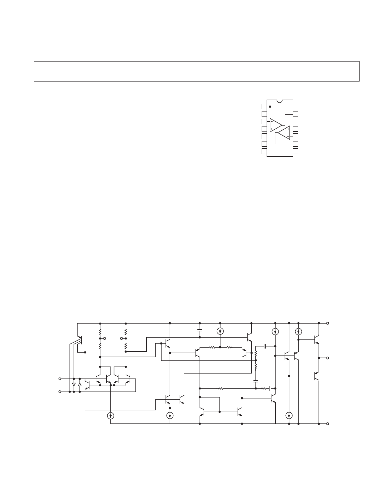
SIMPLIFIED SCHEMATIC
NON
INVERTING
INPUT (+)
INVERTING
INPUT (–)
Q6
Q3
*
R1 AND R2 ARE PREMATURELY ADJUSTED AT WAFER TEST FOR MINIMUM OFFSET VOLTAGE.
R3
NULL
*
R1
Q1A Q1B Q2B Q2A
R4
R2
*
Q21
Q11 Q12
REV. A
Information furnished by Analog Devices is believed to be accurate and
reliable. However, no responsibility is assumed by Analog Devices for its
use, nor for any infringements of patents or other rights of third parties that
may result from its use. No license is granted by implication or otherwise
under any patent or patent rights of Analog Devices.
V+
C2
Q22
R23 R24
Q23 Q24
R5
Q27
One Technology Way, P.O. Box 9106, Norwood, MA 02062-9106, U.S.A.
Tel: 781/329-4700 www.analog.com
Fax: 781/326-8703 © Analog Devices, Inc., 2002
Q28
C1
R9
R12
C3
R11
Q20 Q19
C4
Q26
Q46
OUTPUT
Q45
V-
Page 2

OP227–SPECIFICATIONS
Individual Amplifier Characteristics
(VS = ⴞ15 V, TA = 25ⴗC, unless otherwise noted.)
OP227E OP227G
Parameter Symbol Conditions Min Typ Max Min Typ Max Unit
INPUT OFFSET VOLTAGE V
OS
LONG-TERM VOS STABILITY VOS/Time Notes 2,4 0.2 1.0 0.4 2.0 mV/M
INPUT OFFSET CURRENT I
INPUT BIAS CURRENT I
INPUT NOISE VOLTAGE e
OS
B
n p-p
Note 1 20 80 60 180 mV
O
735 1275nA
± 10 ± 40 ± 15 ± 80 nA
0.1 Hz to 10 Hz 0.08 0.20 0.09 0.28 mV p-p
Notes 3,5
INPUT NOISE VOLTAGE
DENSITY e
INPUT NOISE DENSITY i
n
fO = 10 Hz
f
= 30 Hz
O
fO = 1000 Hz
n
fO = 10 Hz
= 30 Hz
f
O
fO = 1000 Hz
3
3
3, 6
3, 6
3
3, 6
3.5 6.0 3.8 9.0 nV/Hz
3.1 4.7 3.3 5.9 nV/Hz
3.0 3.9 3.2 4.6 nV/Hz
1.7 4.5 1.7 pA/Hz
1.0 2.5 1.0 pA/Hz
0.4 0.7 0.4 0.7 pA/Hz
INPUT RESISTANCE
Differential Mode R
Common Mode R
IN
INCM
Note 7 1.3 6 0.7 4 MW
32GW
INPUT VOLTAGE RANGE IVR ± 11.0 ± 12.3 ± 11.0 ± 12.3 V
COMMON-MODE
REJECTION RATIO CMRR VCM = ± 11 V 114 126 100 120 dB
POWER SUPPLY
REJECTION RATIO PSRR VS = ± 4 V to
± 18 V 1 10 2 20 mV/V
LARGE-SIGNAL
VOLTAGE GAIN A
VO
RL ⱖ 2 kW,
V
= ± 10 V 1000 1800 700 1500 V/mV
O
ⱖ 600 kW,
R
L
VO = ± 10 V 800 1500 600 1500 V/mV
OUTPUT VOLTAGE SWING V
O
RL ⱖ 2 kW±12.0 ± 13.8 ± 11.5 ± 13.5 V
RL ⱖ 600 W±10.0 ± 11.5 ± 10.0 ± 11.5 V
SLEW RATE SR RL ⱖ 2 kW
4
1.7 2.8 1.7 2.8 V/ms
GAIN BANDWIDTH PROD. GBW Note 4 5 8 5 8 MHz
OPEN-LOOP OUTPUT
RESISTANCE R
POWER CONSUMPTION P
O
d
VO = 0, IO = 0 70 70 W
Each Amplifier 90 140 100 170 mW
OFFSET ADJUSTMENT
RANGE Rp = 10 kW±4 ± 4mV
NOTES
1
Input offset voltage measurements are performed by automated test equipment approximately 0.5 seconds after application of power. E Grade specifications are
guaranteed fully warmed up.
2
Long term input offset voltage stability refers to the average trend line of VOS vs. time over extended periods after the first 30 days of operation. Excluding the initial
hour of operation, changes in VOS during the first 30 days are typically 2.5 mV. Refer to the Typical Performance Curve.
3
Sample tested.
4
Parameter is guaranteed by design.
5
See test circuit and frequency response curve for 0.1 Hz to 10 Hz tester.
6
See test circuit for current noise measurement.
7
Guaranteed by input bias current.
Specifications subject to change without notice.
–2–
REV. A
Page 3

SPECIFICATIONS
OP227
Individual Amplifier Characteristics
(VS = ⴞ15 V, –25ⴗC £ TA £ +85ⴗC, unless otherwise noted.)
OP227E OP227G
Parameter Symbol Conditions Min Typ Max Min Typ Max Unit
INPUT OFFSET
VOLTAGE V
OS
Note 1 40 140 85 280 mV
AVERAGE INPUT
OFFSET DRIFT TCV
TCV
OS
OSn
Note 2 0.5 1.0 0.5 1.8 mV/ⴗC
INPUT OFFSET
CURRENT I
OS
10 50 20 135 nA
INPUT BIAS
CURRENT I
B
± 14 ± 60 ± 25 ± 150 nA
INPUT VOLTAGE
RANGE IVR ± 10 ± 11.8 ± 10 ± 11.8 V
COMMON-MODE
REJECTION RATIO CMRR V
= ± 10 V 110 124 96 118 dB
CM
POWER SUPPLY
REJECTION RATIO PSRR V
= ± 4.5 V to
S
± 18 V 2 15 2 32 mV/V
LARGE-SIGNAL
VOLTAGE GAIN A
VO
RL ⱖ 2 kW,
V
= ± 10 V 750 1500 450 1000 V/mV
O
OUTPUT VOLTAGE
SWING V
O
RL ⱖ 2 kW±11.7 ± 13.6 ± 11.0 ± 13.3 V
Matching Characteristics
(VS = ± 15 V, TA = 25ⴗC, unless otherwise noted.)
OP227E OP227G
Parameter Symbol Conditions Min Typ Max Min Typ Max Unit
INPUT OFFSET
VOLTAGE MATCH ⌬V
OS
25 80 55 300 mV
AVERAGE
NONINVERTING Bias
CURRENT I
+
B
II
I
+=
B
++ +
BA BB
2
± 10 ± 40 ± 15 ± 90 nA
NONINVERTING
OFFSET CURRENT IOS+I
+ = IB+A-I
OS
B+B
± 12 ± 60 ± 20 ± 130 nA
INVERTING OFFSET
CURRENT I
-I
OS
- = IB-A-IB-
OS
B
± 12 ± 60 ± 20 ± 130 nA
COMMON-MODE
REJECTION RATIO
MATCH ⌬CMRR V
= ± 11 V 110 123 97 117 dB
CM
POWER SUPPLY
REJECTION RATIO
MATCH ⌬PSRR V
= ± 4 V to
S
± 18 V 2 10 2 20 mV/V
CHANNEL
SEPARATION CS Note 1 126 154 126 154 dB
NOTES
1
Input Offset Voltage measurements are performed by automated equipment approximately 0.5 seconds after application of power.
2
The TCVOS performance is within the specifications unnulled or when nulled with RP = 8 kW to 20 kW, optimum performance is obtained with RP = 8 kW.
3
Sample tested.
Specifications subject to change without notice.
REV. A
–3–
Page 4

OP227–SPECIFICATIONS
Matching Characteristics
(VS = ⴞ15 V, TA = -25ⴗC to +85ⴗC, unless otherwise noted.)
OP227E OP227G
Parameter Symbol Conditions Min Typ Max Min Typ Max Unit
INPUT OFFSET
VOLTAGE MATCH ⌬V
OS
40 140 90 400 mV
INPUT OFFSET
TRACKING TC⌬V
Nulled or Unnulled* 0.3 1.0 0.5 1.8 mV/ⴗC
OS
AVERAGE
NONINVERTING
BIAS CURRENT I
+
B
II
I
+=
B
++ +
BA BB
2
± 14 ± 60 ± 25 ± 170 nA
AVERAGE DRIFT OF
NONINVERTING BIAS
CURRENT TCI
+80180 pA/ⴗC
B
NONINVERTING
OFFSET CURRENT I
+I
OS
+ = IB+A–IB+
OS
B
± 20 ± 90 ± 35 ± 250 nA
AVERAGE DRIFT OF
NONINVERTING
OFFSET CURRENT TCI
+ 130 250 pA/ⴗC
OS
INVERTING OFFSET
CURRENT I
–I
OS
– = IB–A–IB–
OS
B
± 20 ± 90 ± 35 ± 250 nA
COMMON-MODE
REJECTION RATIO
MATCH ⌬CMRR V
= ± 10 V 106 120 90 112 dB
CM
POWER SUPPLY
REJECTION RATIO
MATCH ⌬PSRR V
= ± 4.5 V to ± 18 V 2 15 3 32 mV/V
S
NOTES
*Sample tested.
Specifications subject to change without notice.
–4–
REV. A
Page 5
OP227
WARNING!
ESD SENSITIVE DEVICE
ABSOLUTE MAXIMUM RATINGS
Supply Voltage . . . . . . . . . . . . . . . . . . . . . . . . . . . . . . . . ±22 V
Input Voltage
Output Short-Circuit Duration . . . . . . . . . . . . . . . . . Indefinite
Differential Input Voltage
Differential Input Current
1
. . . . . . . . . . . . . . . . . . . . . . . . . . . . . . . . . . . . . . . . . . . . . . . .
2
. . . . . . . . . . . . . . . . . . . . . . . ±0.7 V
2
. . . . . . . . . . . . . . . . . . . . . ±25 mA
±22 V
Storage Temperature Range . . . . . . . . . . . . . –65∞C to +150∞C
Operating Temperature Range
OP227E, OP227G . . . . . . . . . . . . . . . . . . . . –25∞C to +85∞C
Lead Temperature (Soldering 60 sec) . . . . . . . . . . . . . . 300∞C
NOTES
1
For supply voltages less than ±22 V, the absolute maximum input voltage is equal
to the supply voltage.
2
The OP227 inputs are protected by back-to-back diodes. Current limiting resistors
are not used in order to achieve low noise. If differential input voltage exceeds ±0.7
V, the input current should be limited to 25 mA.
3
is specified for worst-case mounting conditions, i.e.,
JA
in socket for CERDIP package.
is specified for device
JA
THERMAL CHARACTERISTICS
Thermal Resistance
14-Lead CERDIP
3
= 106∞C/W
JA
= 16∞C/W
JC
ORDERING GUIDE
TA = 25ⴗCHermetic Operating
VOS MAX (V) DIP 14-Lead Temperature Range
80 OP227EY IND
180 OP227GY IND
For military processed devices, please refer to the Standard
Microcircuit Drawing (SMD) available at
www.dscc.dla.mil/programs/milspec/default.asp.
SMD Part Number ADI Equivalent
5962-8688701CA
*Not recommended for new design, obsolete April 2002.
*
OP227AYMDA
CAUTION
ESD (electrostatic discharge) sensitive device. Electrostatic charges as high as 4000 V readily
accumulate on the human body and test equipment and can discharge without detection. Although
the OP227 features propriety ESD protection circuitry, permanent damage may occur on devices
subjected to high energy electrostatic discharges. Therefor, proper ESD precautions are
recommended to avoid performance degradation or loss of functionality.
REV. A
–5–
Page 6

OP227
Hz
–Typical Performance Characteristics
BACK-TO-BACK
0.1F
47F
100k⍀
10⍀
D.U.T.
VOLTAGE GAIN
= 50,000
BACK-TO-BACK
2k⍀
5F
10F
TPC 1. Voltage Noise Test Circuit
(0.1 Hz to 10 Hz p-p)
10
9
8
7
6
5
4
3
2
VOLTA GE NOISE DENSITY – nV/ Hz
1
l/f CORNER
= 2.7Hz
1
10 100 1k
FREQUENCY – Hz
TA = 25ⴗC
VS = ⴞ15V
TPC 3. Voltage Noise Density vs.
Frequency
120
OP12
100k⍀
0.1F
24.3k⍀
BACK-TO-BACK
4.3k⍀
4.7F
2.35F
23.5F
SCOPE
R
IN
110k⍀
X 1
= 1M⍀
80
40
0
–40
–80
VOLTA G E NOISE – nV
–120
TPC 2. Low Frequency Noise
(Observation Must Be Limited to 10
Seconds to Ensure 0.1 Hz Cutoff)
100
741
l/f CORNER
10
l/f CORNER
2.7 Hz
VOLTA G E NOISE – nV/ Hz
INSTRUMENTATION
10
1
OP227
RANGE, TO DC
LOW NOISE
AUDIO
OP AMP
l/f CORNER
AUDIO RANGE
10 100 1k
FREQUENCY – Hz
TO 20 kHz
TPC 4. Comparison of Op Amp Voltage
Noise Spectra
1 SEC / DIV
100
90
10
0%
0.1Hz TO 10Hz PEAK-TO-PEAK NOISE
10
1
0.1
rms VOLTAGE NOISE – V
0.01
100
1k 10k 100k
BANDWIDTH – Hz
TPC 5. Input Wideband Noise vs. Bandwidth (0.1 Hz to Frequency Indicated)
T
A
V
S
= 25ⴗC
= ⴞ15V
100
T
= 25ⴗC
A
V
10
AT 10Hz
TOTAL NO ISE – nV/
AT 1kHZ
1
100
= ⴞ15V
S
RESISTOR NOISE ONLY
SOURCE RESISTANCE – ⍀
R1
R2
R
= 2R1
S
1k 10k
TPC 6. Total Noise vs. Source
Resistance
5
VS = ⴞ15V
4
3
2
VOLTA GE NOISE DENSITY – nV/ Hz
1
–50
AT 10Hz
AT 1kHz
–25 0 25 50 75 100 125
TEMPERATURE – ⴗC
TPC 7. Voltage Noise Density vs.
Temperature
–6–
10.0
1.0
l/f CORNER
CURRENT NOISE – pA/ Hz
= 140Hz
0.1
10
100 1k 10k
FREQUENCY – Hz
TPC 8. Current Noise Density vs.
Frequency
REV. A
Page 7

OP227
10
9
8
7
TA = +125ⴗC
6
5
4
(BOTH AMPLIFIERS ON)
SUPPLY CURRENT – mA
3
2
5
TA = +25ⴗC
TA = –55ⴗC
10 15 20 25 30 35 40 45
TOTA L SUPPLY VOLTAGE – V
TPC 9. Supply Current vs. Supply
Voltage
TA = 25ⴗC
V
S
= ⴞ15V
10
OP227G
5
CHANGE IN INPUT OFFSET VOLTAGE – V
0
01 5
TIME AFTER POWER ON – MINUTES
234
TPC 12. Warm-Up Drift
120
100
80
60
40
20
0
–20
–40
OFFSET VOLTAGE – V
–60
–80
–100
–55–35 –15 5 25 45 65 85 105125 145165
–75
TEMPERATURE – ⴗC
TPC 10. Offset Voltage Drift of
Representative Units
30
25
TA = 25ⴗC TA = 70ⴗC
20
15
VOLTA G E – V
10
5
ABSOLUTE CHANGE IN INPUT OFFSET
0
–20
DEVICE IMMERSED
IN 70ⴗ C OIL BATH
020406080100
TIME – Sec
VS = ⴞ15V
THERMAL
SHOCK
RESPONSE
BAND
TPC 13. Offset Voltage Change Due to
Thermal Shock
5
4
3
2
1
0
–1
–2
–3
–4
OFFSET VOLTAGE DRIFT WITH TIME – V
–5
2345678910
0
11112
0.2V/MO.
0.2V/MO.
0.2V/MO.
TIME – MONTHS
TPC 11. Offset Voltage Stability
with Time
50
VS = ⴞ15V
40
30
20
10
INPUT BIAS CURRENT – nA
0
–25 0 25 50 75 100 125 150
–50
TEMPERATURE – ⴗC
TPC 14. Input Bias Current vs.
Temperature
50
VS = ⴞ15V
40
30
20
10
INPUT OFFSET CURRENT – nA
0
–50 –25 0 25 50 75 100 125
–75
TEMPERATURE – ⴗC
TPC 15. Input Offset Current vs.
Temperature
REV. A
130
110
90
70
50
30
OPEN-LOOP GAIN – dB
10
–10
1
10 100 1k 10k 100k 1M 10M 100M
FREQUENCY – Hz
TPC 16. Open-Loop Gain vs. Frequency
–7–
70
⌽M
60
GBW
50
PHASE MARGIN – DEG
4
3
SLEW
2
SLEW RATE – V/s
–50 –25 0 25 50 75 100 125
–75
TEMERATURE – ⴗC
VS = ⴞ15V
10
9
8
7
8
TPC 17. Slew Rate, Gain Bandwidth
Product, Phase Margin vs. Temperature
GAINBANDWIDTH PRODUCT – MHz
Page 8

OP227
25
20
15
10
5
GAIN – dB
0
–5
10
1M
GAIN
PHASE
MARGIN
= 70ⴗ
10M 100M
FREQUENCY – Hz
TA = 25ⴗC
V
S
= ⴞ15V
80
100
120
140
160
180
200
220
TPC 18. Gain, Phase Shift vs.
Frequency
28
24
20
16
12
8
4
PEAK-TO-PEAK OUTPUT VOLTAGE – V
0
1k
10k 100k 1M 10M
FREQUENCY – Hz
TA = 25ⴗC
V
S
= ⴞ15V
TPC 21. Maximum Undistorted Output
vs. Frequency
2.5
2.0
TA = 25ⴗC
1.5
1.0
PHASE SHIFT – DEG
OPEN-LOOP GAIN – V/V
0.5
0.0
0
10 20 30 40 50
TOTA L SUPPLY VOLTAGE – V
= 2k⍀
R
L
RL = 1k⍀
TPC 19. Open-Loop Gain vs. Supply
Voltage
100
80
60
40
PERCENT OVERSHOOT
20
0
0
500 1000 1500 2000 2500
CAPACITIVE LOAD – pF
VS = 615V
VIN = 100mV
AV = +1
TPC 22. Small-Signal Overshoot vs.
Capacitive Load
18
16
14
POSITIVE
12
10
8
6
4
OUTPUT SWING – V
2
0
–2
SWING
TS = 25ⴗC
VS = ⴞ15V
100
NEGATIVE
SWING
LOAD RESISTANCE – ⍀
1k 10k
TPC 20. Output Swing vs. Resistive
Load
60
50
40
30
20
SHORT-CIRCUIT CURRENT – mA
20
01 5
lSC(–)
lSC(+)
TIME FROM OUTPUT SHORTED TO
234
GROUND – MINUTES
T
A
= ⴞ15V
V
S
= ⴞ25ⴗ
TPC 23. Short-Circuit Current vs. Time
100
90
10
0%
= +1, CL= 15pF
A
VCL
V
= ⴞ15V
S
T
= 25ⴗC
A
20mV
+50mV
0V
–50mV
TPC 24. Small-Signal Transient
Response
500ns
100
90
10
0%
A
VCL
V
S
T
A
= +1
= ⴞ15V
= 25ⴗC
2V
+5V
0V
–5V
TPC 25. Large-Signal Transient
Response
2s
140
120
100
⌬CMMR – dB
80
60
1k
10k 100k 1M 10M
FREQUENCY – Hz
TPC 26. Matching Characteristic
CMRR Match vs. Frequency
–8–
REV. A
Page 9

OP227
16
COMMON-MODE RANGE – V
–12
–16
12
8
4
0
–4
–8
TA = +25ⴗC
0
TA = –55ⴗC
TA = –55ⴗC
TA = +125ⴗC
ⴞ5 ⴞ10 ⴞ15
SUPPLY VOLTAGE – V
TA = +125ⴗC
TA = +25ⴗC
ⴞ20
TPC 27. Common-Mode Input Range
vs. Supply Voltage
100
80
60
40
20
0
–20
–40
–60
–80
OFFSET VOLTAGE MATCH – V
–100
–120
–75
–55–35 –15 5 25 45 65 85 105125145 165
TEMPERATURE – ⴗC
2.4
2.2
2.0
1.8
1.6
1.4
1.2
1.0
0.8
OPEN-LOOP VOLTAGE GAIN – V/V
0.6
0.4
100
1k 10k 100k
LOAD RESISTANCE – ⍀
TA = 25ⴗC
VS = ⴞ15V
TPC 28. Open-Loop Voltage Gain vs.
Load Resistance
40
30
20
10
NONINVERTING BIAS CURRENT – ⴞnA
0
–35 –15 5 25 45 65 85 105 125
–55
TEMPERATURE – ⴗC
140
120
100
PSSR – dB
PSRR (+)
80
⌬
PSRR (–)
60
PSRR AND
40
20
1
10 100 1k 10k 100k 1M
FREQUENCY – Hz
⌬ PSRR (–)
⌬ PSRR (+)
TPC 29. PSRR and ⌬PSRR vs.
Frequency
50
40
30
20
OFFSET CURRENT – ⴞnA
10
–35 –15 5 25 45 6585105125
–55
TEMPERATURE – ⴗC
TPC 30. Matching Characteristic:
Drift of Offset Voltage Match of
Representative Units
125
120
115
⌬ CMRR – dB
110
105
–55
–35 –15
525456585105 125
TEMPERATURE – ⴗC
TPC 33. Matching Characteristic:
CMRR Match vs. Temperature
TPC 31. Matching Characteristic:
Average Noninverting Bias Current
vs. Temperature
180
140
120
100
80
CHANNEL SEPARATION – dB
60
100
1k 10k 100k 1M 10M
FREQUENCY – Hz
TPC 34. Channel Separation vs.
Frequency
TPC 32. Matching Characteristic:
Average Offset Current vs. Temperature (Inverting or Noninverting)
REV. A
–9–
Page 10

OP227
BASIC CONNECTIONS
V+(A)
10k⍀
21 14
3
(–)
INPUTS
(+)
(+)
INPUTS
(–)
A
4
OP227
11
B
10
98 7
10k⍀
V+(A)
13
OUT (A)
12
V–(A)
5
V–(B)
6
OUT (B)
Figure 1. Offset Nulling Circuit
APPLICATIONS INFORMATION
Noise Measurements
To measure the 80 nV peak-to-peak noise specification of the
OP227 in the 0.1 Hz to 10 Hz range, the following precautions
must be observed:
•The device must be warmed up for at least five minutes. As
shown in the warm-up drift curve, the offset voltage typically
changes 4 mV due to increasing chip temperature after power-up.
In the 10-second measurement interval, these temperatureinduced effects can exceed tens-of-nanovolts.
∑
For similar reasons, the device must be well shielded from air
currents. Shielding minimizes thermocouple effects.
∑
Sudden motion in the vicinity of the device can also “feedthrough”
∑
The test time to measure 0.1 Hz to 10 Hz noise should not
to increase the observed noise.
exceed 10-seconds. As shown in the noise-tester frequencyresponse curve, the 0.1 Hz corner is defined by only one zero
to eliminate noise contributions from the frequency band
below 0.1 Hz.
∑
A noise-voltage-density test is recommended when measuring
noise on a large number of units. A 10 Hz noise-voltagedensity measurement will correlate well with a 0.1 Hz to 10 Hz
peak-to-peak noise reading, since both results are determined
by the white noise and the location of the 1/f corner frequency.
Instrumentation Amplifier Applications of the OP227
The excellent input characteristics of the OP227 make it ideal
for use in instrumentation amplifier configurations where low
level differential signals are to be amplified. The low noise, low
input offsets, low drift, and high gain, combined with excellent
CMR provide the characteristics needed for high performance
instrumentation amplifiers. In addition, CMR versus frequency
is very good due to the wide gain bandwidth of these op amps.
The circuit of Figure 2 is recommended for applications where
the common-mode input range is relatively low and differential
gain will be in the range of 10 to 1000. This two op amp
instrumentation amplifier features independent adjustment of
common-mode rejection and differential gain. Input impedance is very high since both inputs are applied to non-inverting
op amp inputs.
R0
R2R1
R4
A2
R4R3R3
V
d
]
+
–
( )
R4
V
O
R2
V
CM
R1
V
– 1/2V
CM
VCM + 1/2V
VO =
d
d
R4
1
1+
[ ( )
R3
2
A1
R2R1R3
+
V1
R3
R2 + R3
+
R0
R4
Figure 2. Two Op Amp Instrumentation Amplifier Configuration
The output voltage VO, assuming ideal op amps, is given in
Figure 2. the input voltages are represented as a common-mode
input, V
, plus a differential input, Vd. The ratio R3/R4 is
CM
made equal to the ratio R2/R1 to reject the common mode input
. The differential signal VO is then amplified according to:
V
CM
Ê
R
V
=++
O
R
RRRR
4
1
Á
3
Ë
3423 342
ˆ
+
V where
,
˜
R
O
d
¯
RRR
=
R
1
Note that gain can be independently varied by adjusting RO.
From considerations of dynamic range, resistor tempco matching, and matching of amplifier response, it is generally best to
make R1, R2, R3, and R4 approximately equal. Designing R1,
R2, R3, and R4 as R
allows the output equation to be further
N
simplified:
V
=+
O
Ê
Á
Ë
ˆ
R
N
V where R R R R R
,
˜
dN
R
¯
O
= ===21
123 4
–10–
REV. A
Page 11

OP227
Dynamic range is limited by A1 as well as A2. The output of A1
is:
Ê
V
12=+
Á
Ë
ˆ
R
N
VV
˜
R
¯
O
+–
dCM1
If the instrumentation amplifier was designed for a gain of 10
and maximum V
of ± 1 V, then RN/RO would need to be four
d
and VO would be a maximum of ± 10 V. Amplifier A1 would have
a maximum output of ± 5 V plus 2 VCM, thus a limit of ± 10 V
on the output of A1 would imply a limit of ± 2.5 V on V
nominal value of 10 kW for R
A range of 20 W to 2.5 kW for R
is suitable for most applications.
N
will then provide a gain range
O
CM
. A
of 10 to 1000. The current through RO is Vd/RO, so the amplifiers
must supply ± 10 mV/20 W (or ± 0.5 mA) when the gain is at the
maximum value of 1000 and V
is at ± 10 mV.
d
Rejecting common-mode inputs is important in accurately
amplifying low level differential signals. Two factors determine
the CMR in this instrumentation amplifier configuration (assuming
infinite gain):
∑
CMR of the op amps
∑
Matching of the resistor network ratios (R3/R4 = R2/R1)
In this instrumentation amplifier configuration error due to CMR
effect is directly proportional to the CMR match of the op
For the OP227, this DCMR is a minimum of 97 dB for the
amps.
“G”
and 110 dB for the “E” grades. A DCMR value of 100 dB and a
common-mode input range of ± 2.5 V indicates a peak inputreferred error of only ± 25 mV. Resistor matching is the other
factor affecting CMR. Defining A
as the differential gain of the
d
instrumentation amplifier and assuming that R1, R2, R3, and R4
are approximately equal (RN will be the nominal value), then CMR
for this instrumentation amplifier configuration will be approximately A
divided by 4⌬R/RN. CMR at differential gain of 100
d
would be 88 dB with resistor matching of 0.01%. Trimming R1
to make the ratio R3/R4 equal to R2/R1 will raise the CMR
until limited by linearity and resistor stability considerations.
The high open-loop gain of the OP227 is very important to
achieving high accuracy in the two op amp instrumentation
amplifier configuration. Gain error can be approximated by:
A
Gain Error
1
A
d
+
1
A
O
2
AA
2
OO
d
11
<,
1
where Ad is the instrumentation amplifier differential gain and
is the open loop gain of op amp A2. This analysis assumes
A
O2
equal values of R1, R2, R3, and R4. For example, consider an
OP227 with A
of 700 V/mV. Id the differential gain Ad were
O2
set to 700, then the gain error would be 1/1.001, which is
approximately 0.1%.
Another effect of finite op amp gain is undesired feedthrough of
common-mode input. Defining A
as the open-loop gain of op
O1
amp A1, then the common-mode error (CME) at the output
due to this effect would be approximately:
A
REV. A
CME
2
1
+
d
,
AAA
d
2
O
1
V
CM
1
O
–11–
For Ad/A01 < 1, this simplifies to (2Ad/A01) 3 VCM. If the op amp
gain is 700 V/mV, V
is 2.5 V, and Ad is set to 700, then the
CM
error at the output due to this effect will be approximately 5 mV.
A compete instrumentation amplifier designed for a gain of 100
is shown in Figure 3. It has provision for trimming of input
voltage, CMR, and gain. Performance is excellent due to
offset
the high
fiers combined
gain, high CMR, and low noise of the individual ampli-
with the tight matching characteristics of the
OP227 dual.
CMR
10k⍀
0.1%
50⍀
9.95k⍀
3
– 1/2V
V
CM
d
GAIN
V
– 1/2V
CM
d
4
2.5k⍀
191⍀
10
11
OFFSET
10k⍀
21 14
OP227
10k⍀, 0.1%
10k⍀, 0.1%
ADJUST
V+
13
12
7
6
5
V–
V+
V
V–
= 100V
O
d
Figure 3. Two Op Amp Instrumentation Amplifier Using
OP227 Dual
A three op amp instrumentation amplifier configuration using
the OP227 and OP27 is recommended for applications requiring high accuracy over a wide gain range. This circuit provides
excellent CMR over a wide frequency range. As with the two op
amp instrumentation amplifier circuits, the tight matching of the
two op amps within the OP227 package provides a real boost in
performance. Also, the low noise, low offset, and high gain of
the individual op amps minimize errors.
A simplified schematic is shown in Figure 4. The input stage
(A1 and A2) serves to amplify the differential input V
amplifying the common-mode voltage V
. The output stage
CM
without
d
then rejects the common-mode input. With ideal op amps and
no resistor matching errors, the outputs of each amplifier will
be:
Ê
V
1
=+
–
Á
1
Ë
Ê
V
=+
–
Á
2
Ë
==+
VVV
O
21
=
VAV
Odd
1
–
R
21
R
O
21
R
R
O
ˆ
V
d
V
+
˜
¯
ˆ
˜
¯
Ê
Á
Ë
1
V
2
d
2
+
V
21
R
R
O
CM
CM
ˆ
˜
¯
V
d
Page 12

OP227
The differential gain Ad is 1 + 2R1/R0 and the common-mode
input V
is rejected.
CM
While output error due to input offsets and noise are easily
determined, the effects of finite gain and common-mode rejection are more subtle. CMR of the complete instrumentation
amplifier is directly proportioned to the match in CMR of the
input op amps. This match varies from 97 dB to 110 dB minimum for the OP227. Using 100 dB, then the output response to
a common-mode input V
VAV
[]
would be:
CM
=¥10
O
CM
dCM
5–
CMRR of the instrumentation amplifier, which is defined as
20 log10A
, is simply equal to the ⌬CMRR of the OP227.
d/ACM
While this ⌬CMRR is already high, overall CMRR of the
complete amplifier can be raised by trimming the output stage
resistor network.
Finite gain of the input op amps causes a scale factor error and a
small degradation in CMR. Designating the open-loop gain of
op amp A
as AO1, and op amp A2 as AO2, then the following
1
equation approximates output:
ˆ
˜
¯
Ê
AV
Á
dd
Á
Ë
V
O
++
1
1
Ê
R
1011
Á
RA A
Ë
12
OO
Ê
R
21011
+
RA A
–
Á
Ë
12
OO
ˆ
ˆ
V
˜
˜
CM
˜
¯
¯
This can be simplified by defining AO as the nominal open-loop
gain and ⌬A0 as the differential open-loop gain. Then:
Ê
1
+
1
R
101
RA
V
O
O
AV
Á
dd
Ë
+
R
21
R
0
A
D
O
2
A
O
ˆ
V
˜
CM
¯
The high open-loop gain of each amplifier within the OP227
(700,000 minimum at 25∞C in R
accuracy even at high values of A
≥ 2 kW) assures good gain
L
. The effect of finite open-
d
loop gain on CMR can be approximated by:
2
A
CMRR
O
A
D
O
If ⌬AO/AO were 6% and AO were 600,000, then the CMRR due to
finite gain of the input op amps would be approximately 140 dB.
R1
2R1
= (1 +
) Vd
R0
R2
OP27
A3
R2
V
O
V
– 1/2V
CM
VCM + 1/2V
V
1/2
OP227
A1
d
R0
R1
1/2
OP227
A2
d
O
R2
V1
R2
V2
Figure 4. Three Op Amp Instrumentation Amplifier Using
OP227 and OP27
The unity-gain output stage contributes negligible error to the
overall amplifier. However, matching of the four resistor R2
network is critical to achieving high CMR. Consider a worstcase situation where each R2 resistor had an error of ± ⌬R2. If
the resistor ratio is high on one side and low on the other, then
the common-mode gain will be 2⌬R2/2⌬R2. Since the output
stage gain is unity, CMRR will then be R2/2⌬R2. It is common
practice to maximize overall CMRR for the total instrumentation amplifier circuit.
–12–
REV. A
Page 13

OP227
High Speed Precision Rectifier
The low offsets and excellent load driving capability of the OP27
are key advantages in this precision rectifier circuit. The summing
impedances can be as low as 1 kW which helps to reduce the
effects of stray capacitance.
For positive inputs, D2 conducts and D1 is biased OFF. Amplifiers A1 and A2 act as a follower with output-to-output feedback
and the R1 resistors are not critical. For negative inputs, D1
conducts and D2 is biased OFF. A1 acts as a follower and A2
serves as a precision inverter. In this mode, matching of the two
R1 resistors is critical to gain accuracy.
C
1
30pF
A1 A2
V
1
A1, A2: OP27
Figure 5. High Speed Precision Rectifier
Typical component values are 30 pF for C1 and 2 kW for R3.
The drop across D1 must be less than the drop across the FET
diode D2. A 1N914 for D1 and a 2N4393 for the JFET were
used successfully.
The circuit provides full-wave rectification for inputs of up to
± 10 V and up to 20 kHz in frequency. To assure frequency stability,
be sure to decouple the power supply inputs and minimize any
capactive loading. An OP227, which is two OP27 amplifiers in a
single package, can be used to improve packaging density.
D
1
1N914
R
*
1
1k⍀
2N4393
R
2k⍀
*
D
2
3
MATCHED
R
1k⍀
*
2
V
O
REV. A
–13–
Page 14

OP227
OUTLINE DIMENSIONS
14-Lead Ceramic Dip – Glass Hermetic Seal [CERDIP]
(Q-14)
Dimensions shown in inches and (millimeters)
0.005 (0.13) MIN
PIN 1
0.200 (5.08)
0.200 (5.08)
0.125 (3.18)
CONTROLLING DIMENSIONS ARE IN INCHES; MILLIMETERS DIMENSIONS
(IN PARENTHESES) ARE ROUNDED-OFF INCH EQUIVALENTS FOR
REFERENCE ONLY AND ARE NOT APPROPRIATE FOR USE IN DESIGN
0.785 (19.94) MAX
MAX
0.023 (0.58)
0.014 (0.36)
0.098 (2.49) MAX
14
17
0.100 (2.54) BSC
8
0.070 (1.78)
0.030 (0.76)
0.310 (7.87)
0.220 (5.59)
0.060 (1.52)
0.015 (0.38)
SEATING
PLANE
0.150
(3.81)
MIN
0.320 (8.13)
0.290 (7.37)
15
0
0.015 (0.38)
0.008 (0.20)
–14–
REV. A
Page 15

OP227
Revision History
Location Page
10/02—Data Sheet changed from REV. 0 to REV. A.
Edits to GENERAL DESCRIPTION . . . . . . . . . . . . . . . . . . . . . . . . . . . . . . . . . . . . . . . . . . . . . . . . . . . . . . . . . . . . . . . . . . . . . . . . 1
OP227A and OP227F deleted from Individual Amplifier Characteristics section . . . . . . . . . . . . . . . . . . . . . . . . . . . . . . . . . . . . . . . 2
OP227A and OP227F deleted from Matching Characteristics section . . . . . . . . . . . . . . . . . . . . . . . . . . . . . . . . . . . . . . . . . . . . . . . . 3
Edits to ABSOLUTE MAXIMUM RATINGS . . . . . . . . . . . . . . . . . . . . . . . . . . . . . . . . . . . . . . . . . . . . . . . . . . . . . . . . . . . . . . . . . 5
Edits to ORDERING GUIDE . . . . . . . . . . . . . . . . . . . . . . . . . . . . . . . . . . . . . . . . . . . . . . . . . . . . . . . . . . . . . . . . . . . . . . . . . . . . . . 5
Updated OUTLINE DIMENSIONS . . . . . . . . . . . . . . . . . . . . . . . . . . . . . . . . . . . . . . . . . . . . . . . . . . . . . . . . . . . . . . . . . . . . . . . 14
REV. A
–15–
Page 16

C02685–0–10/02(A)
–16–
PRINTED IN U.S.A.
 Loading...