

Page 1
Dual Low Power Operational Amplifier,
8
7
6
5
1
2
3
4
NC = NO CONNECT
+IN A
V–
+IN B
–IN A
OUT A
V+
OUT B–IN B
a
FEATURES
Excellent TCV
Low Input Offset Voltage, 150 V Max
Low Supply Current, 550 A Max
Single Supply Operation, 5 V to 30 V
Low Input Offset Voltage Drift, 0.75 V/ⴗC
High Open-Loop Gain, 1500 V/mV Min
High PSRR, 3 V/V
Wide Common-Mode Voltage
Range, V– to within 1.5 V of V+
Pin Compatible with 1458, LM158, LM2904
Available in Die Form
GENERAL DESCRIPTION
The OP221 is a monolithic dual operational amplifier that can
be used either in single or dual supply operation. The wide
supply voltage range, wide input voltage range, and low supply
current drain of the OP221 make it well-suited for operation
from batteries or unregulated power supplies.
The excellent specifications of the individual amplifiers combined
with the tight matching and temperature tracking between channels
Match, 2 V/ⴗC Max
OS
Single or Dual Supply
OP221
PIN CONNECTIONS
8-Lead SOIC
(S-Suffix)
provide high performance in instrumentation amplifier designs.
The individual amplifiers feature very low input offset voltage,
low offset voltage drift, low noise voltage, and low bias current.
They are fully compensated and protected.
Matching between channels is provided on all critical parameters
including input offset voltage, tracking of offset voltage vs. temperature, non-inverting bias currents, and common-mode rejection.
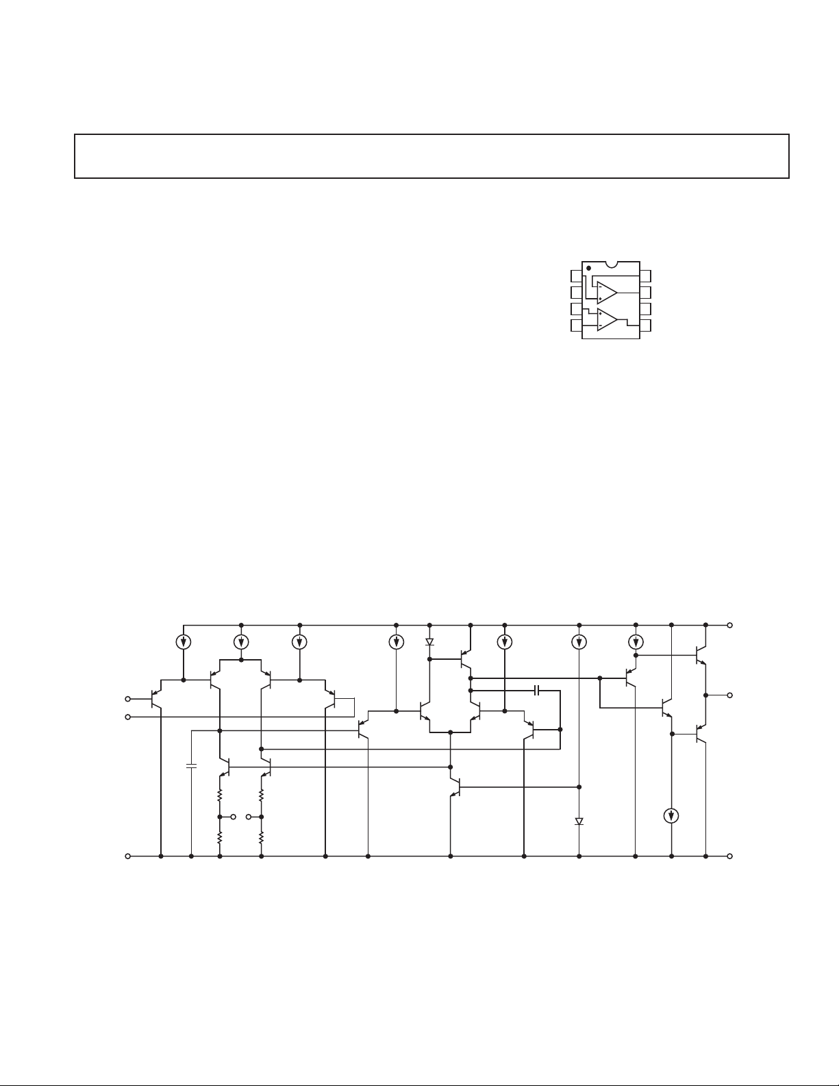
SIMPLIFIED SCHEMATIC
Q3 Q4
–IN
+IN
Q1
Q5
*
NULL
*
ACCESSIBLE IN CHIP FORM ONLY
Q2
Q7
Q6
REV. C
Information furnished by Analog Devices is believed to be accurate and
reliable. However, no responsibility is assumed by Analog Devices for its
use, nor for any infringements of patents or other rights of third parties that
may result from its use. No license is granted by implication or otherwise
under any patent or patent rights of Analog Devices.
V+
Q11
Q12
Q26
Q9 Q10
Q4
Q13
Q33
One Technology Way, P.O. Box 9106, Norwood, MA 02062-9106, U.S.A.
Tel: 781/329-4700 www.analog.com
Fax: 781/326-8703 © Analog Devices, Inc., 2002
Q28
OUTPUT
Q27
Q29
V–
Page 2

OP221–SPECIFICATIONS
(Electrical Characteristics at Vs = ⴞ2.5 V to ⴞ15 V, TA = 25ⴗC, unless otherwise noted.)
OP221G
Parameter Symbol Conditions Min Typ Max Unit
Input Offset Voltage V
OS
250 500 mV
Input Offset Current Ios VCM = 0 1.5 7 nA
Input Bias Current I
B
Input Voltage Range IVR V+ = 5 V, V– = 0 V
VCM = 0 70 120 nA
1
V
= ± 15 V –15/13.5
S
0/3.5
V
Common-Mode CMRR V+ = –5 V, V– = 0 V
Rejection Ratio 0 V £ V
= ± 15 V dB
V
S
–15 V £ V
Power Supply PSRR VS = ± 2.5 V to ± 15 V 32 100
Rejection Ratio V– = 0 V, V+ = 5 V to 30 V 57 180
£ 3.5 V 75 85
CM
£ 13.5 V 80 90
CM
mV/V
Large-Signal Avo VS = ±15 V, RL = 10 kW
Voltage Gain V
Output Voltage V
O
Swing R
= ±10 V 800 V/mV
O
V+ = 5 V, V– = 0 V 0.8/4 V
= 10 kW
L
VS = 15 V, RL = 10 kW±13.5
Slew Rate SR RL = 10 kW
2
0.2 0.3 V/mS
Bandwidth BW 600 kHz
Supply Current I
SY
(Both Amplifiers) VS = ± 15 V, No Load 850 900
VS = ± 2.5 V, No Load 550 650
mA
–2–
REV. C
Page 3

OP221
SPECIFICATIONS
(Electrical Characteristics at VS = ⴞ2.5 V to ⴞ15 V, –40ⴗC £ TA £ +85ⴗC, unless otherwise noted.)
OP221G
Parameter Symbol Conditions Min Typ Max Unit
Average Input TCV
Offset Voltage Drift
1
Input Offset Voltage V
Input Offset Current I
Input Bias Current I
OS
B
OS
OS
VCM = 0 2 10 nA
VCM = 0 80 140 nA
Input Voltage Range IVR V+ = 5 V, V– = 0 V
V
= ± 15 V –15/13.2
S
2
0/3.2
23 mV/∞C
400 700 mV
V
Common-Mode CMRR V+ = –5 V, V– = 0 V
Rejection Ratio 0 V £ V
V
= ±15 V dB
S
–15 V £ V
Power Supply PSRR VS = ± 2.5 V to ± 15 V 57 180
Rejection Ratio V– = 0 V, V+ = 5 V to 30 V 100 320
Large-Signal A
VO
Voltage Gain V
Output Voltage V
O
Swing R
VS = ±15 V, RL = 10 kW
O
V+ = 5 V, V– = 0 V 0.9/3.7
L
£ 3.5 V 70 80
CM
£ 13.5 V 75 85
CM
= ±10 V 600
= 10 kW V
mV/V
V/mV
VS = 15 V, RL = 10 kW 13.2
Supply Current I
SY
VS = ± 2.5 V, No Load 600 750 mA
(Both Amplifiers) VS = ± 15 V, No Load 950 1000
NOTES
1
Sample tested.
2
Guaranteed by CMRR test limits.
Matching Characteristics at Vs = ⴞ15 V, TA = 25ⴗC, unless otherwise noted.
OP221G
Parameter Symbol Conditions Min Typ Max Unit
Input Offset
Voltage Match DV
OS
250 600 mV
Average Noninverting
Bias Current IB+ 120 nA
Noninverting Input I
+410nA
OS
Offset Current
Common-Mode
Rejection Ratio DCMRR V
1
Match
= –15 V to 13.5 V 72 dB
CM
Power Supply
Rejection Ratio DPSRR V
2
Match
NOTES
1
DCMRR is 20 log10 VCM/DCME, where V
2
DPSRR is: Input-Referred Differential Error
DV
S
is the voltage applied to both noninverting inputs and DCME is the difference in common-mode input-referred error.
CM
= ± 2.5 V to ± 15 V 140 mV/V
S
REV. C
–3–
Page 4

(Matching Characteristics at Vs = ⴞ15 V, –40ⴗC £ TA £ +85ⴗC for OP221G, unless other-
OP221–SPECIFICATIONS
.
wise noted. G is sample tested.)
OP221G
Parameter Symbol Conditions Min Typ Max Unit
Input Offset
Voltage Match DV
Average Noninverting I
B
OS
+V
= 0 140 nA
CM
400 800 mV
Bias Current
Input Offset ICDV
OS
35mV∞C
Voltage Tracking
Noninverting Input I
+V
OS
= 0 6 12 nA
CM
Offset Current
Common-Mode
Rejection Ratio DCMRR V
1
Match
= –15 V to 13.2 V 72 80 dB
CM
Power Supply
Rejection Ratio DPSRR 140 mV/V
2
Match
NOTES
1
DCMRR is 20 log10 VCM/DCME, where V
2
DPSRR is: Input-Referred Differential Error
DV
S
is the voltage applied to both noninverting inputs and DCME is the difference in common-mode input-referred error.
CM
–4–
REV. C
Page 5

OP221
WARNING!
ESD SENSITIVE DEVICE
ABSOLUTE MAXIMUM RATINGS (Note 1)
Supply Voltage . . . . . . . . . . . . . . . . . . . . . . . . . . . . . . . . ± 18 V
Differential Input Voltage . . . . . . . . . .30 V or Supply Voltage
Input Voltage . . . . . . . . . . . . . . . . . . . . . . . . . . Supply Voltage
Output Short-Circuit Duration . . . . . . . . . . . . . . . . Indefinite
Storage Temperature Range . . . . . . . . . . . . –65∞C to +150∞C
Operating Temperature Range
OP221G . . . . . . . . . . . . . . . . . . . . . . . . . . . . –40∞C to +85∞C
Lead Temperature (Soldering 60 sec) . . . . . . . . . . . . . . 300∞C
Junction Temperature (T
) . . . . . . . . . . . . . –65∞C to +150∞C
J
Package Type JA (Note 2)
JC
Unit
8-Lead SOIC(S) 158 43 ∞C/W
NOTES
1
Absolute maximum ratings apply to both DICE and packaged parts, unless
otherwise noted.
2
is specified for device soldered to printed circuit board for SOIC package.
JA
ORDERING GUIDE
TA = +25ⴗC Operating Package
V
MAX Plastic Temperature Options
OS
(V) 8-Lead Range
150
150
300
500
500
500 OP221GS XIND RN-8
Figure 1. Dice Characteristics
CAUTION
ESD (electrostatic discharge) sensitive device. Electrostatic charges as high as 4000 V readily
accumulate on the human body and test equipment and can discharge without detection. Although
the OP221 features proprietary ESD protection circuitry, permanent damage may occur on devices
subjected to high-energy electrostatic discharges. Therefore, proper ESD precautions are
recommended to avoid performance degradation or loss of functionality.
REV. C
–5–
Page 6

OP221–Typical Perfomance Characteristics
140
120
100
dc
10Hz
80
60
10 0H z
1kHz
140
120
100
dc
10Hz
80
60
10 0Hz
1kHz
140
120
100
T
= 25ⴗC
A
RL = 15k⍀
80
60
40
OPEN-LOOP GAIN – dB
VS = ⴞ15V
20
0
–25 0 25 50 75 100 125
–50
TEMPERATURE – ⴗC
TPC 1. Open-Loop Gain at ±15 V vs.
Temperature
120
100
80
60
40
OPEN-LOOP GAIN – dB
20
0
0.1
VS = ⴞ5V
110100 1k 10k 100k 1M 10M
FREQUENCY – Hz
VS = ⴞ15V
TPC 4. Open-Loop Gain at ±15 V vs.
Frequency
40
OPEN-LOOP GAIN – dB
VS = ⴞ15V
20
0
–25 0 25 50 75 100 125
–50
TEMPERATURE – ⴗC
TPC 2. Open-Loop Gain at ± 5 V vs.
Temperature
70
60
50
40
30
20
10
CLOSED-LOOP GAIN – dB
0
–10
110
100
1k 10k 100k 1M 10M
FREQUENCY – Hz
TPC 5. Closed-Loop Gain vs.
Frequency
40
OPEN-LOOP GAIN – dB
20
0
0
ⴞ5 ⴞ10 ⴞ15
SUPPLY VOLTAGE – V
TPC 3. Open-Loop Gain at vs.
Supply Voltage
25
PHASE
TA = 25ⴗC
= ⴞ15V
V
S
20
15
10
VOLTA G E GAIN – dB
–5
–10
⵰m = 42ⴗ
5
GAIN
0
100k 1M 10M
FREQUENCY – Hz
TPC 6. Gain and Phase Shift vs.
Frequency
80
100
120
140
160
180
PHASE SHIFT – Degrees
200
220
55
50
45
Degrees
40
PHASE MARGIN –
0.35
SLEW RATE
0.30
0.25
V/sec
SLEW RATE –
0.20
–25 0 25 50 75 100 125
–50
PHASE MARGIN
GAIN BANDWIDTH
TEMPERATURE – ⴗC
VS = ⴞ15V
TPC 7. Phase Margin, Gain Bandwidth,
and Slew Rate vs. Temperature
850k
800k
750k
700k
650k
120
100
80
60
PSRR – dB
GAIN BANDWIDTH – Hz
40
20
0
T
A
V
= ⴞ15V
S
10
–PSRR
= 25ⴗC
100 1k 10k 100k
FREQUENCY – Hz
TPC 8. PSRR vs. Frequency
+PSRR
120
100
80
60
CMRR – Hz
40
20
0
1
10 100
FREQUENCY – Hz
TA = 25ⴗC
V
S
1k 10k 100k
TPC 9. CMRR vs. Frequency
= ⴞ15V
–6–
REV. C
Page 7

30
28
24
20
16
12
8
PEAK-TO-PEAK AMPLITUTDE – V
4
0
1K 1M
10k 100k
FREQUENCY – Hz
TA = 25ⴗC
V
= ⴞ15V
S
R
= 10k⍀
L
TPC 10. Maximum Output Swing
vs. Frequency
16
TA = 25ⴗC
14
V
= ⴞ15V
S
12
10
MAXIMUM OUTPUT – V
POSITIVE
8
6
4
2
0
100 100k
LOAD RESISTANCE – ⍀
NEGATIVE
1k 10k
TPC 11. Maximum Output Voltage
vs. Load Resistance
OP221
TA = 25ⴗC
2.0
V
= ⴞ2.5V
S
1.0
MAXIMUM OUTPUT – V
0
100 100k1k 10k
LOAD RESISTANCE – ⍀
TPC 12. Maximum Output Voltage
vs. Load Resistance
NEGATIVE
POSITIVE
100
80
70
60
50
40
30
20
VOLTAGE NOISE – nV/ Hz
10
11k10 100
FREQUENCY – Hz
TPC 13. Voltage Noise Density vs.
Frequency
10
1.0
CURRENT NOISE – pA Hz
0.1
11k
10 100
FREQUENCY – Hz
TPC 13. Current Noise Density vs.
Frequency
REV. C
–7–
Page 8

OP221
Figure 2a. Noninverting Step Response
Figure 2b. Noninverting Step Response
INPUT
OUTPUT
10k⍀
Figure 3a. Inverting Step Response
Figure 3b. Inverting Step Response
10k⍀
INPUT
10k⍀
OUTPUT
Figure 4. Noninverting Test Circuit
–8–
Figure 5. Inverting Test Circuit
REV. C
Page 9

OP221
SPECIAL NOTES ON THE APPLICATION OF DUAL
MATCHED OPERATIONAL AMPLIFIERS
Advantages of Dual Monolithic Operational Amplifiers
Dual matched operational amplifiers provide the engineer with a
powerful tool for designing instrumentation amplifiers and many
other differential-input circuits. These designs are based on the
principle that careful matching between two operational amplifiers
can minimize the effect of dc errors in the individual amplifiers.
Reference to the circuit shown in Figure 6, a differential-in,
differential-out amplifier, shows how the reductions in error can
be accomplished. Assuming the resistors used are ideally matched,
the gain of each side will be identical. If the offset voltages of
each amplifier are perfectly matched, then the net differential
voltage at the amplifier’s output will be zero. Note that the output
offset error of this amplifier is not a function of the offset voltage
of the individual amplifiers, but only a function of the difference
(degree of matching) between the amplifiers’ offset voltages. This
error-cancellation principle holds for a considerable number of
input referred error parameters—offset voltage, offset voltage
drift, inverting and noninverting bias currents, common mode
and power supply rejection ratios. Note also that the impedances
of each input, both common-mode and differential-mode, are
high and tightly matched, an important feature not practical with
single operation amplifier circuits.
R3
R1
+
INPUT
–
SIDE
‘A’
OP221
R2
SIDE
‘R’
R4
+
OUTPUT
–
Figure 6. Differential-In, Differential-Out Amplifier
INSTRUMENTATION AMPLIFIER APPLICATIONS
Two-Op Amp Configuration
The two-op amp circuit (Figure 7) is recommended where the
common-mode input voltage range is relatively limited; the
common-mode and differential voltage both appear at V1. The
high open-loop gain of the OP221 is very important in achieving
good CMRR in this configuration. Finite open-loop gain of A1
(Ao1) causes undesired feedthrough of the common-mode input.
For Ad/Ao, << 1, the common-mode error (CME) at the output due to this effect is approximately (2 Ad/Ao1) x VCM. This
circuit features independent adjustment of CMRR and differential gain.
Three-Op Amp Configuration
The three-op amp circuit (Figure 8) has increased commonmode voltage range because the common-mode voltage is not
amplified as it is in Figure 7. The CMR of this amplifier is directly
proportional to the match of the CMR of the input op amps. CMRR
can be raised even further by trimming the output stage resistors.
R0
GAIN
ADJ
R1
V
– 1/2V
CM
D
–
V
d
+
V
+ 1/2V
CM
D
R4
1 +
V
=
O
R3
R2
V1
R3
R2 + R3
R0
AD = 2 1+
R4
OP221
A2
Vd +
1/2
OP221
A1
1
R3
R2
+
2
R1
+
R4
IF R1 = R2 = R3 = R4, THEN VO = 2 1 +
1/2
R1
R0
– ADVD
V
O
R4
R2
R3
–
R3
VCM
R1
R4
R1
V
D
R0
Figure 7. Two-Op Amp Circuit
R1
V
– 1/2V
CM
–
V
d
+ 1/2V
V
CM
A1
D
OP221
R0
R1
V+
A2
–
D
OP221
V–
1/2
1/2
VO = 2 1 +
R2
V1
R2
V2
R2
2R1
R2
V+
OP221
A3
V–
V
D
R0
V
O
Figure 8. Three-Op Amp Circuit
REV. C
–9–
Page 10

OP221
OUTLINE DIMENSIONS
8-Lead Standard Small Outline Package [SOIC]
Narrow Body
(RN-8)
Dimensions shown in millimeters and (inches)
5.00 (0.1968)
4.80 (0.1890)
4.00 (0.1574)
3.80 (0.1497)
85
6.20 (0.2440)
5.80 (0.2284)
41
1.27 (0.0500)
0.25 (0.0098)
0.10 (0.0040)
COPLANARITY
0.10
CONTROLLING DIMENSIONS ARE IN MILLIMETERS; INCH DIMENSIONS
(IN PARENTHESES) ARE ROUNDED-OFF MILLIMETER EQUIVALENTS FOR
REFERENCE ONLY AND ARE NOT APPROPRIATE FOR USE IN DESIGN
BSC
SEATING
PLANE
COMPLIANT TO JEDEC STANDARDS MS-012AA
1.75 (0.0688)
1.35 (0.0532)
0.51 (0.0201)
0.33 (0.0130)
0.25 (0.0098)
0.19 (0.0075)
0.50 (0.0196)
0.25 (0.0099)
8ⴗ
0ⴗ
1.27 (0.0500)
0.41 (0.0160)
ⴛ 45ⴗ
–10–
REV. C
Page 11

OP221
Revision History
Location Page
10/02—Data Sheet changed from REV. B to REV. C.
Deleted 8-Lead CERDIP Package (Q-8) . . . . . . . . . . . . . . . . . . . . . . . . . . . . . . . . . . . . . . . . . . . . . . . . . . . . . . . . . . . . . . . .Universal
Edits to SPECIFICATIONS . . . . . . . . . . . . . . . . . . . . . . . . . . . . . . . . . . . . . . . . . . . . . . . . . . . . . . . . . . . . . . . . . . . . . . . . . . . . . 2–4
Edits to ABSOLUTE MAXIMUM RATINGS . . . . . . . . . . . . . . . . . . . . . . . . . . . . . . . . . . . . . . . . . . . . . . . . . . . . . . . . . . . . . . . . . 5
Edits to ORDERING GUIDE . . . . . . . . . . . . . . . . . . . . . . . . . . . . . . . . . . . . . . . . . . . . . . . . . . . . . . . . . . . . . . . . . . . . . . . . . . . . . . 5
Updated OUTLINE DIMENSIONS . . . . . . . . . . . . . . . . . . . . . . . . . . . . . . . . . . . . . . . . . . . . . . . . . . . . . . . . . . . . . . . . . . . . . . . 10
6/02—Data Sheet changed from REV. A to REV. B.
Edits to 8-Lead SOIC Package (R-8) . . . . . . . . . . . . . . . . . . . . . . . . . . . . . . . . . . . . . . . . . . . . . . . . . . . . . . . . . . . . . . . . . . . . . . . . 10
09/01—Data Sheet changed from REV. 0 to REV. A.
Edits to PIN CONNECTIONS . . . . . . . . . . . . . . . . . . . . . . . . . . . . . . . . . . . . . . . . . . . . . . . . . . . . . . . . . . . . . . . . . . . . . . . . . . . . . 1
Global deletion of references to OP221B and OP221C . . . . . . . . . . . . . . . . . . . . . . . . . . . . . . . . . . . . . . . . . . . . . . . . . . . . . . . 2, 3, 4
Edits to WAFER TEST LIMITS . . . . . . . . . . . . . . . . . . . . . . . . . . . . . . . . . . . . . . . . . . . . . . . . . . . . . . . . . . . . . . . . . . . . . . . . . . . 4
Edits to ABSOLUTE MAXIMUM RATINGS . . . . . . . . . . . . . . . . . . . . . . . . . . . . . . . . . . . . . . . . . . . . . . . . . . . . . . . . . . . . . . . . . 5
Edits to ORDERING GUIDE . . . . . . . . . . . . . . . . . . . . . . . . . . . . . . . . . . . . . . . . . . . . . . . . . . . . . . . . . . . . . . . . . . . . . . . . . . . . . . 5
Edits to PACKAGE TYPE . . . . . . . . . . . . . . . . . . . . . . . . . . . . . . . . . . . . . . . . . . . . . . . . . . . . . . . . . . . . . . . . . . . . . . . . . . . . . . . . 5
REV. C
–11–
Page 12

C00324–0–10/02(C)
–12–
PRINTED IN U.S.A.
 Loading...