

Page 1
OUT A
–IN A
+IN A
V–
V+
OUT B
–IN B
+IN B
1
2
3
4
5
6
7
8
OP220
Dual Micropower
+IN A
V–
+IN B
–IN B
–IN A
OUT A
V+
OUT B
1
2
3
4
5
6
7
8
a
FEATURES
Excellent TCV
Low Input Offset Voltage: 150 V Max
Low Supply Current: 100 A
Single-Supply Operation: 5 V to 30 V
Low Input Offset Voltage Drift: 0.75 V/ⴗC Max
High Open-Loop Gain: 2,000 V/mV
High PSRR: 3 V/V
Low Input Bias Current: 12 nA
Wide Common-Mode Voltage Range: V– to Within
1.5 V of V+
Pin Compatible with 1458, LM158, and LM2904
Available in Die Form
GENERAL DESCRIPTION
The OP220 is a monolithic dual operational amplifier that can
be used either in single or dual supply operation. The low offset
voltage and input offset voltage tracking as low as 1.0 mV/∞C,
make this the first micropower precision dual operational amplifier.
The excellent specifications of the individual amplifiers combined with the tight matching and temperature tracking between
channels provides high performance in instrumentation amplifier designs. The individual amplifiers feature extremely low
input offset voltage, low offset voltage drift, low noise voltage,
and low bias current. They are fully compensated and protected.
Matching between channels is provided on all critical parameters
including input offset voltage, tracking of offset voltage versus
temperature, noninverting bias currents, and common-mode
rejection ratios.
Match: 2 V/ⴗC Max
OS
Operational Amplifier
PIN CONFIGURATIONS
8-Lead Hermatic Dip
(Z-Suffix)
8-Lead SOIC
(S-Suffix)
OP220
8-Lead Plastic Dip
(P-Suffix)
OUT A
1
OP220
–IN A
2
+IN A
3
V–
4
8-Lead TO-99
(J-Suffix)
8
7
6
5
V+
OUT B
–IN B
+IN B
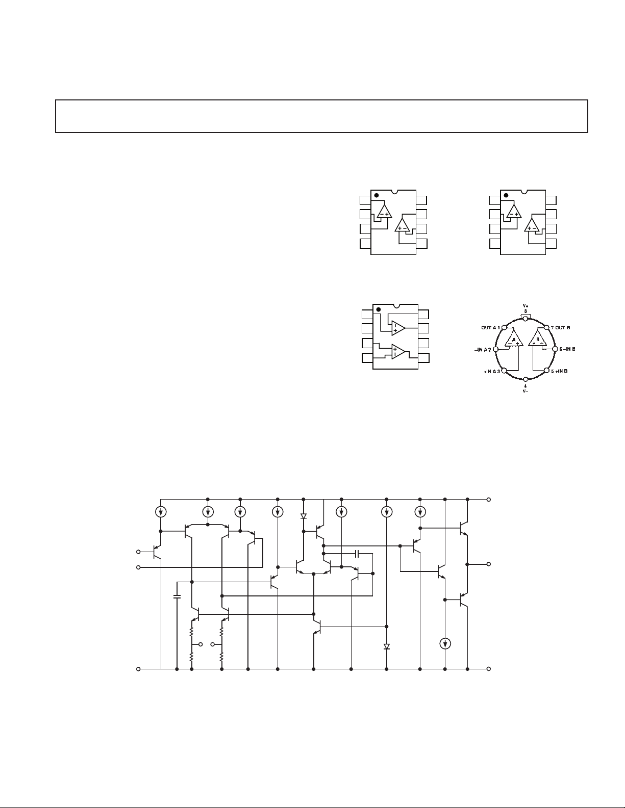
V+
Q11
Q27
Q28
OUTPUT
Q29
V–
Q3 Q4
–IN
+IN
Q1
Q5
NULL*
*ACESSIBLE IN CHIP FORM ONLY
REV. A
Information furnished by Analog Devices is believed to be accurate and
reliable. However, no responsibility is assumed by Analog Devices for its
use, nor for any infringements of patents or other rights of third parties that
may result from its use. No license is granted by implication or otherwise
under any patent or patent rights of Analog Devices.
Q2
Q7
Q6
Figure 1. Simplified Schematic
Q12
Q26
Q9
Q10
Q8
Q13
Q33
One Technology Way, P.O. Box 9106, Norwood, MA 02062-9106, U.S.A.
Tel: 781/329-4700 www.analog.com
Fax: 781/326-8703 © Analog Devices, Inc., 2002
Page 2

OP220–SPECIFICA TIONS
ELECTRICAL CHARACTERISTICS
Parameter Symbol Conditions Min Typ Max Min Typ Max Min Typ Max Unit
Input Offset Voltage V
Input Offset Current I
Input Bias Current I
Input Voltage Range IVR V+ = 5 V, V– = 0 V 0/3.5 0/3.5 0/3.5 V
Common-Mode CMRR V+ = 5 V, V– = 0 V 90 100 85 90 75 85 dB
Rejection Ratio 0 V £ VCM £ 3.5 V
Power Supply PSRR V
Rejection Ratio V– = 0 V, V+ = 5 V to 30 V 6 18 18 57 57 180 mV/V
Large-Signal A
Voltage Gain RL = 100 kW,
Output Voltage V
Swing RL = 10 kW
Slew Rate* SR RL =25 kW 0.05 0.05 0.05 V/ms
Bandwidth BW A
Supply Current I
(Both Amplifiers) VS = ± 15 V, No Load 140 170 150 190 205 220 mA
OS
OS
B
VO
O
SY
VS = ± 2.5 V to ± 15 V 120 150 250 300 500 750 mV
VCM = 0 0.15 1.5 0.2 2 0.2 3.5 nA
VCM = 0 12 201325 1430nA
VS = ± 15 V –15/+13.5 –15/+13.5 –15/+13.5 V
VS = ± 15 V 95 100 90 95 80 90 dB
–15 V £ VCM £ +13.5 V
= ± 2.5 V to ± 15 V, 3 10 10 32 32 100 mV/V
S
V+ = 5 V, V– = 0 V, 500 1,000 500 800 300 500 V/mV
1 V £ VO £ 3.5 V
VS = ± 15 V, RL = 25 kW 1,000 2,000 1,000 2,000 800 1,600 V/mV
VO = ± 10 V
V+ = 5 V, V– = 0 V 0.7/4 0.7/4 0.8/4 V
VS = ± 15 V, RL = 25 kW±14 ± 14 ± 14 V
= 1, RL =25 kW 200 200 200 kHz
VCL
VS = ± 2.5 V, No Load 100 115 115 125 125 135 mA
(@ VS = ⴞ2.5 V to ⴞ15 V, TA = 25ⴗC, unless otherwise noted.)
OP220A/E OP220F OP220C/G
*Sample tested.
(Vs = ⴞ2.5 V to ⴞ15 V, –55ⴗC £ TA £ +125ⴗC for OP220A/C, –25ⴗC £ TA £ +85ⴗC for OP220E/F,
ELECTRICAL CHARACTERISTICS
Parameter Symbol Conditions Min Typ Max Min Typ Max Min Typ Max Unit
Input Offset Voltage TCV
Drift*
Input Offset Voltage V
Input Offset Current I
Input Bias Current I
Input Voltage Range IVR V+ = 5 V, V– = 0 V 0/3.2 0/3.2 0/3.2 V
Common-Mode CMRR V+ = 5 V, V– = 0 V 86 90 80 85 70 80 dB
Rejection Ratio 0 V £ VCM £ 3.2 V
Power Supply PSRR VS = ± 2.5 V to ± 15 V, 6 18 18 57 57 180 mV/V
Rejection Ratio V– = 0 V, V+ = 5 V to 30 V 10 32 32 100 100 320 mV/V
Large-Signal A
Voltage Gain VO = ± 10 V
Output Voltage V
Swing RL = 20 kW
Supply Current I
(Both Amplifiers) VS = ± 15 V, No Load 190 250 200 280 275 330 mA
OS
OS
B
VO
O
SY
VS = ± 15 V 0.75 1.5 1.2 2 2 3 mV/∞C
OS
VCM = 0 0.5 2 0.6 2.5 0.6 5 nA
VCM = 0 12 251330 1440nA
VS = ± 15 V –15/+13.2 –15/+13.2 –15/+13.2 V
VS = ± 15 V 90 958590 7585 dB
–15 V £ VCM £ +13.2 V
VS = ± 15 V, RL = 50 kW 500 1,000 500 800 400 500 V/mV
V+ = 5 V, V– = 0 V 0.9/3.8 0.9/3.8 1.0/3.8 V
VS = ± 15 V, RL = 50 kW±13.6 ± 13.6 ± 13.6 V
VS = ± 2.5 V, No Load 135 170 155 185 170 210 mA
–40ⴗC £ TA £ +85ⴗC for OP220G unless otherwise noted.)
OP220A/E OP220F OP220C/G
200 300 400 500 1,000 1,300 mV
*Sample tested.
–2–
REV. A
Page 3

OP220
MATCHING CHARACTERISTICS
(@ VS = ⴞ15 V, TA = 25ⴗC, unless otherwise noted.)
OP220A/E OP220F OP220C/G
Parameter Symbol Conditions Min Typ Max Min Typ Max Min Typ Max Unit
Input Offset Voltage DV
OS
150 300 250 500 300 800 mV
Match
Average Noninverting I
+V
B
= 0 10 2015252030nA
CM
Bias Current
Noninverting Offset I
+VCM = 0 0.7 1.5 1 2 1.4 2.5 nA
OS
Current
Common-Mode DCMRR VCM = –15 V to +13.5 V 92 100 87 95 72 85 dB
Rejection Ratio Match
Power Supply DPSRR VS = ± 2.5 V to ± 15 V, 6 14 18 44 57 140 mV/V
Rejection Ratio Match
NOTES
1
DCMRR is 20 log10 VCM/DCME, where VCM is the voltage applied to both noninverting inputs and D CME is the difference in common-mode input-referred error.
2
DPSRR is
3
Sample tested.
Input Referred Differential Error
DV
1
2
S
.
(Vs = ⴞ15 V, –55ⴗC £ TA £ +125ⴗC for OP220A/C, –25ⴗC £ TA £ +85ⴗC for OP220E/F,
MATCHING CHARACTERISTICS
Parameter Symbol Conditions Min Typ Max Min Typ Max Min Typ Max Unit
Input Offset Voltage DV
Match
Input Offset Voltage TCDV
1
Tracking
Average Noninverting IB+V
Bias Current
Average Drift of TCIB+VCM = 0 15 2515303050pA/∞C
Noninverting
Bias Current
1
Noninverting Offset IOS+VCM = 0 0.7 2 1 2.5 2.5 5 nA
Current
Average Drift of TCIOS+VCM = 0 7 15 12 22.5 15 30 pA/∞C
Noninverting Offset
1
Current
Common-Mode DCMRR VCM = –15 V to +13 V 87 96 82 96 72 80 dB
Rejection Ratio Match
Power Supply DPSRR VS = ± 2.5 V to ± 15 V, 10 26 30 78 57 250 mV/V
Rejection Ratio Match
NOTES
1
Sample tested.
2
DCMRR is 20 log10 VCM/DCME, where VCM is the voltage applied to both noninverting inputs and D CME is the difference in common-mode input-referred error.
3
DPSRR is
Input Referred Differential Error
DV
OS
OS
= 0 10 2515302240nA
CM
2
3
S
.
–40ⴗC £ TA £ +85ⴗC for OP220G unless otherwise noted. Grades E, F are sample tested.)
OP220A/E OP220F OP220C/G
250 500 400 800 800 1,800 mV
12 1.5 3 1.5 5 mV/∞C
TYPICAL ELECTRICAL CHARACTERISTICS
(@ Vs = ⴞ15 V, TA = 25ⴗC, unless otherwise noted.)
OP220N
Parameter Symbol Conditions Typical Unit
Average Input Offset Voltage Drift TCV
Large-Signal Voltage Gain A
VO
REV. A
OS
RL = 25 kW 2000 V/mV
–3–
1.5 mV/∞C
Page 4
OP220–SPECIFICA TIONS
ABSOLUTE MAXIMUM RATINGS*
Supply Voltage . . . . . . . . . . . . . . . . . . . . . . . . . . . . . . . . ± 18 V
Differential Input Voltage . . . . . . . . . .30 V or Supply Voltage
Input Voltage . . . . . . . . . . . . . . . . . . . . . . . . . . Supply Voltage
Output Short-Circuit Duration Indefinite
Storage Temperature Range . . . . . . . . . . . . –65∞C to +150∞C
Junction Temperature (T
) . . . . . . . . . . . . . –65∞C to +150∞C
i
Operating Temperature Range
OP220A/OP220C . . . . . . . . . . . . . . . . . . –55∞C to +125∞C
OP220E/OP220F . . . . . . . . . . . . . . . . . . . . –25∞C to +85∞C
OP220G . . . . . . . . . . . . . . . . . . . . . . . . . . . –40∞C to +85∞C
Lead Temperature Range (Soldering, 60 sec) . . . . . . . . 300∞C
NOTES
*Absolute Maximum Ratings apply to packaged parts, unless otherwise noted.
DIE CHARACTERISTICS
1. INVERTING INPUT (A)
2. NONINVERTING INPUT (A)
3. BALANCE (A)
4. V–
5. BALANCE (B)
6. NONINVERTING INPUT (B)
7. INVERTING INPUT (B)
8. BALANCE (B)
9. V+
10. OUT (B)
11. V+
12. OUT (A)
13. V+
DIE SIZE 0.097 INCH ⴛ 0.063 INCH, 6111 SQ. MILS
(2.464 mm ⴛ 1.600 mm, 3.94 SQ. mm)
NOTE : ALL V+ PADS ARE INTERNALL CONNECTED
14. BALANCE (A)
Package Type
*
JA
JC
Unit
8-Lead Hermetic DIP (Q) 148 16 ∞C/W
8-Lead Plastic DIP (N) 103 43 ∞C/W
8-Lead SOL (RN) 158 43 ∞C/W
TO-99 (H) 150 18 ∞C/W
*
is specified for worst-case mounting conditions, i.e., JA is specified for device
JA
in socket for CERDIP and PDIP packages; JA is specified for device soldered to
printed circuit board for SO packages.
ORDERING GUIDE
TA = 25∞C Package Options Operating
MAX Temperature
V
OS
(mV) CERDIP Plastic TO-99 Range
150 OP220AZ* MIL
150 OP220EZ* IND
300 OP220FZ* IND
750 OP220CJ* MIL
750 OP220GZ* OP220GP* XIND
750 OP220GS XIND
For military processed devices, please refer to the Mil Standard
Data Sheet
OP220AJ/883*.
*Not for new design. Obsolete April 2002.
WAFER TEST LIMITS
(@ VS = ⴞ2.5 V, to ⴞ15 V, TA = 25ⴗC, unless otherwise noted.)
OP220N
Parameter Symbol Conditions Limit Unit
Input Offset Voltage V
Input Offset Voltage Match ⌬V
Input Offset Current I
Input Bias Current I
OS
B
OS
OS
VCM = 0 2 nA Max
VCM = 0 25 nA Max
200 mV Max
300 mV Max
Input Voltage Range IVR VS = ± 15 V –15/13.5 V Min
Common-Mode CMRR V– = 0 V, V+ = 5 V, 0 V £ V
£ 3.5 V 88 dB Min
CM
Rejection Ratio –15 V £ VCM £ 13.5 V, VS = ± 15 V 93
Power Supply PSRR V
= ± 2.5 V to ± 15 V 12.5 mV/V Max
S
Rejection Ratio V– = 0 V, V+ = 5 V to 30 V 22.5
Large-Signal A
VO
RL = 25 kW, VS = ± 15 V 1000 V/mV Min
Voltage Gain VO = ± 10 V
Output Voltage Swing V
O
V+ = 5 V, V– = 0 V, RL = 10 kW 0.7/4 V Min
VS = ± 15 V, RL = 25 kW±14
Supply Current I
SY
VS = ± 2.5 V, No Load 125 mA Max
(Both Amplifiers) VS = ± 15 V, No Load 190
NOTE
Electrical tests are performed at wafer probe to the limits shown. Due to variations in assembly methods and normal yield loss, yield after packing is not guaranteed
for standard product dice. Consult factory to negotiate specifications based on die lot qualification through sample lot assembly and testing.
–4–
REV. A
Page 5

INPUT OFFSET VOLTAGE – V
TEMPERATURE – ⴗC
14
0
–100 150
INPUT BIAS CURRENT – nA
–50 0 50 100
12
10
8
6
4
2
VS = 15V
–100
150
100
–50
Typical Performance Characteristics–
VS = 15V
50
0
OP220
–150
–50 125–25
0255075100
TEMPERATURE – ⴗC
TPC 1. Normalized Offset Voltage vs. Temperature
80
TA = 25ⴗC
60
40
20
0
–20
⌬ INPUT OFFSET VOLTAGE – V
–40
–60
0
4 8 12 16
POWER SUPPLY VOLTAGE – V
20
TPC 2. Input Offset Voltage vs. Power Supply Voltage
110
VS = 15V
100
90
80
70
60
50
40
OPEN-LOOP GAIN – dB
30
20
10
0
–75 125–50
–25 0 25 50 75 100
10Hz
100Hz
1kHz
TEMPERATURE – ⴗC
TPC 3. Open-Loop Gain vs. Temperature
TPC 4. Input Bias Current vs. Temperature
700
VS = 15V
600
500
400
300
200
INPUT OFFSET CURRENT – pA
100
0
–100 150
–50 0 50 100
TEMPERATURE – ⴗC
TPC 5. Input Offset Current vs. Temperature
200
180
160
140
120
100
SUPPLY CURRENT – A
80
60
0
TA = 125ⴗC
TA = 25ⴗC
TA = –55ⴗC
7.5 10.0 12.5
5.02.5 15.0
SUPPL Y V OL T A GE – V
TPC 6. Supply Current vs. Supply Voltage
17.5
REV. A
–5–
Page 6

OP220
k
k
FREQUENCY – Hz
160
0
0.01 1M0.1
OPEN-LOOP GAIN – dB
1101001k10k 100k
140
80
60
40
20
120
100
TA = 25ⴗC
V
S
= 15V
GAIN
PHASE
⌽m = 53ⴗ
0
45
90
135
180
PHASE SHIFT – Degrees
120
100
80
60
CMRR – dB
40
20
TA = 25ⴗC
V
= 15V
S
0
0.01 1
130
120
110
100
90
80
PSRR – dB
70
60
50
40
1100
17
15
10
5
PEAK OUTPUT VOLTAGE – V
0
110010
TPC 9. Maximum Output Voltage vs. Load Resistance
0.1
110100
FREQUENCY – Hz
TPC 7. CMRR vs. Frequency
–PSRR
10
100 1k 10k
FREQUENCY – Hz
TPC 8. PSRR vs. Frequency
TA = 25ⴗC
V
LOAD RESISTANCE – k⍀
+PSRR
VS = 15V
= 5V
S
TPC 10. Open-Loop Voltage Gain and Phase vs. Frequency
36
T
A
V
S
= 25ⴗC
= 15V
TA = 25ⴗC
32
= 15V
V
S
28
24
20
16
12
8
PEAK-TO-PEAK AMPLITUDE – V
4
0
100 1M1k
10k 100k
FREQUENCY – Hz
TPC 11. Maximum Output Swing vs. Frequency
0.09
0.08
0.07
0.06
sec
0.05
0.04
0.03
SLEW RATE – V/
0.02
0.01
0
–75 150–50 –25 0 25 50 75 100 125
TPC 12. Slew Rate vs. Temperature
VS = 15V
VS = 5V
TEMERATURE – ⴗC
–6–
REV. A
Page 7

OP220
k
k
1,000
100
VOLTAGE NOISE DENSITY – nV/ Hz
10
0.1 1
110100
FREQUENCY – Hz
TPC 13. Voltage Noise Density vs. Frequency
10
Hz
1
0.1
CURRENT NOISE DENSITY – pA/
0.01
0.1 1
110100
FREQUENCY – Hz
TPC 14. Noise Density vs. Frequency
REV. A
–7–
Page 8

OP220
T
25k⍀
2s
OUTPU
100pF
INPUT
100
90
10
0%
50mV
20mV
OP220
Figure 2. Small-Signal Transient Response
2V
100
90
200s
R0
GAIN
R1 R2
V
– 1/2 V
CM
D
–
V
D
+ 1/2 V
È
4
Í
3
Î
1
+
D
12213
RRR
Ê
Á
Ë
V
CM
R
V
=+ +
ODCM
R
If then,
1234 21
=== =+
RRRR V
1/2
OP220
4
R
A1
R3
RR
ˆ
+
˜
¯
OD
ADJ
V1
23043342
+
R
Ê
Á
Ë
R4
A2
1/2
OP220
˘
RRRRR
Ê
+-
V
˙
˚
1
R
0
R
Á
Ë
ˆ
V
˜
¯
V
R
O
ˆ
V
˜
¯
1
Figure 4. Two Op Amp Instrumentation Amplifier
Configuration
The input voltages are represented as a common-mode input
plus a differential input VD. The ratio R3/R4 is made equal
V
CM
to the ratio R2/R, to reject the common-mode input V
differential signal V
is then amplified according to:
D
CM
. The
10
0%
5V
INPUT
OUTPUT
C
L
100pF
10k⍀
OP220
40k⍀
R
L
25k⍀
Figure 3. Large-Signal Transient Response
INSTRUMENTATION AMPLIFIER APPLICATIONS OF
THE OP220
Two Op Amp Configuration
The excellent input characteristics of the OP220 make it ideal for
use in instrumentation amplifier configurations where low-level
differential signals are to be amplified. The low-noise, low input
offsets, low drift, and high gain combined with excellent CMRR
provide the characteristics needed for high-performance instrumentation amplifiers. In addition, the power supply current
drain is very low.
The circuit of Figure 4 is recommended for applications where
the common-mode input range is relatively low and differential
gain will be in the range of 10 to 1,000. This two op amp instrumentation amplifier features independent adjustment of common-mode
rejection and differential gain. Input impedance is very high since
both inputs are applied to noninverting op amp inputs.
Ê
R
V
4
=++
O
R
3
3423 342
RRRR
1
Á
Ë
ˆ
+
R
O
˜
¯
V
D
,where
RRR
=
R
1
Note that gain can be independently varied by adjusting RO.
From considerations of dynamic range, resistor tempco matching, and matching of amplifier response, it is generally best to
make RX, R2, R3, and R4 approximately equal. Designating
R1, R2, R3, and R4 as RN allows the output equation to be
further simplified:
V
=+
O
Ê
Á
Ë
ˆ
R
N
VRRRRR
˜
DN
R
¯
O
=== =21 1 2 3 4,where
Dynamic range is limited by A1 as well as A2; the output of A1 is:
V
11 2=- +
Ê
Á
Ë
ˆ
R
N
VV
˜
DCM
R
¯
O
+
If the instrumentation amplifier were designed for a gain of 10
and maximum V
would be a maximum of ± 10 V. Amplifier A1 would
and V
O
have a maximum output of ± 5 V plus 2 V
± 10 V on the output of A1 would imply a limit of ±2.5 V on V
A nominal value of 100 kW for R
tions. A range of 200 W to 25 kW for R
range of 10 to 1,000. The current through R
of ± 1 V, then RN/RO would need to be four
D
, thus a limit of
CM
is suitable for most applica-
N
will then provide a gain
O
is VD/RO, so the
O
CM
.
amplifiers must supply ± 10 mV/200 W when the gain is at the
maximum value of 1,000 and V
is at ± 10 mV.
D
Rejecting common-mode inputs is most important in accurately
amplifying low-level differential signals. Two factors determine
the CMR of this instrumentation amplifier configuration (assuming
infinite gain):
1. CMRR of the op amps
2. Matching of the resistor network (R3/R4 = R2/R1)
–8–
REV. A
Page 9

OP220
V
R
R
V
V
V
R
R
V
V
VVV
R
R
V
VAV
O
D
CM
O
D
CM
O
O
D
ODD
11
21
2
21
21
2
211
21
=- +
Ê
Ë
Á
ˆ
¯
˜
+
=+
Ê
Ë
Á
ˆ
¯
˜
+
=-=+
Ê
Ë
Á
ˆ
¯
˜
=
In this instrumentation amplifier configuration, error due to
CMRR effect is directly proportional to the differential CMRR
of the op amps. For the OP220A/E, this combined CMRR is a
minimum of 98 dB. A combined CMRR value of 100 dB and
common-mode input range of ± 2.5 V indicates a peak inputreferred error of only ± 25 mV.
Resistor matching is the other factor affecting CMRR. Defining
Ad as the differential gain of the instrumentation amplifier and
assuming that R1, R2, R3 and R4 are approximately equal (R
N
will be the nominal value), then CMRR will be approximately
divided by 4DR/RN. CMRR at differential gain of 100 would
A
D
be 88 dB with resistor matching of 0.1%. Trimming R1 to make
the ratio R3/R4 equal to R2/R1 will directly raise the CMRR
until it is limited by linearity and resistor stability considerations.
The high open-loop gain of the OP220 is very important in
achieving high accuracy in the two-op-amp instrumentation
amplifier configuration. Gain error can be approximated by:
GainError =
1
A
+
1
A
A
D
<
,
AA
2
D
01 02
02
1
where AD is the instrumentation amplifier differential gain and
A
is the open-loop gain of op amp A2. This analysis assumes
02
equal values of R1, R2, R3, and R4. For example, consider an
OP220 with A
of 700 V/mV. If the differential gain AD were
02
set to 700, the gain error would be 1/1.001 which is approximately 0.1%.
Another effect of finite op amp gain is undesired feedthrough of
common-mode input. Defining A
as the open-loop gain of op
01
amp A1, then the common-mode error (CME) at the output
due to this effect will be approximately:
THREE OP AMP CONFIGURATION
A three op amp instrumentation amplifier configuration using
the OP220 and OP777 is recommended for applications requiring
high accuracy over a wide gain range. This circuit provides
excellent CMR over a wide input range. As with the two op amp
instrumentation amplifier circuits, tight matching of the two op
amps provides a real boost in performance.
R1
V
– 1/2 V
CM
D
–
R0 A3
V
D
+ 1/2 V
V
CM
+
D
1/2
OP220
1/2
OP220
A1
R1
V+
A2
V–
V
O
R2
V1
R2
V2
= VD 1 +
V–
R2
2R1
R0
R2
V+
OP777
V
O
Figure 5. Three Op Amp Instrumentation Amplifier Using
OP220 and OP777
A simplified schematic is shown in Figure 2. The input stage
(A1 and A2) serves to amplify the differential input V
amplifying the common-mode voltage V
. The output stage
CM
without
D
then rejects the common-mode input. With ideal op amps and
no resistor matching errors, the outputs of each amplifier will be:
For AD/A01, < 1, this simplifies to (2 AD/A01) ⫻ VCM. If the op
amp gain is 700 V/mV, V
the error at the output due to this effect will be approximately 5 mV.
The OP220 offers a unique combination of excellent dc performance, wide input range, and low supply current drain that is
particularly attractive for instrumentation amplifier design.
REV. A
A
1
CME
D
=
A
+21
A
is 2.5 V, and AD is set to 700, then
CM
V
CM
A
D
01
01
The differential gain AD is 1 + 2R1/RO and the common-mode
input V
is rejected.
CM
This three op amp instrumentation amplifier configuration using an
OP220 at the input and an OP777 at the output provides excellent
performance over a wide gain range with very low power consumption. A gain range of 1 to 2,000 is practical and CMR of over
120 dB is readily achievable.
–9–
Page 10

OP220
OUTLINE DIMENSIONS
8-Lead Ceramic DIP – Glass Hermatic Seal [CERDIP]
(Q-8)
Dimensions shown in inches and (millimeters)
0.005 (0.13)
PIN 1
0.200 (5.08)
MAX
0.200 (5.08)
0.125 (3.18)
0.023 (0.58)
0.014 (0.36)
CONTROLLING DIMENSIONS ARE IN INCH; MILLIMETERS DIMENSIONS
(IN PARENTHESES) ARE ROUNDED-OFF MILLIMETER EQUIVALENTS FOR
REFERENCE ONLY AND ARE NOT APPROPRIATE FOR USE IN DESIGN
0.055 (1.40)
MIN
0.100 (2.54) BSC
0.405 (10.29) MAX
MAX
85
1
4
0.070 (1.78)
0.030 (0.76)
0.310 (7.87)
0.220 (5.59)
0.060 (1.52)
0.015 (0.38)
0.150 (3.81)
MIN
SEATING
PLANE
0.320 (8.13)
0.290 (7.37)
15
0
0.015 (0.38)
0.008 (0.20)
8-Lead Plastic Dual-in-Line Package [PDIP]
(N-8)
Dimensions shown in inches and (millimeters)
8-Lead Standard Small Outline Package [SOIC]
Narrow Body
(RN-8)
Dimensions shown in millimeters and (inches)
5.00 (0.1968)
4.80 (0.1890)
4.00 (0.1574)
3.80 (0.1497)
0.25 (0.0098)
0.10 (0.0040)
COPLANARITY
0.10
CONTROLLING DIMENSIONS ARE IN MILLIMETERS; INCH DIMENSIONS
(IN PARENTHESES) ARE ROUNDED-OFF MILLIMETER EQUIVALENTS FOR
REFERENCE ONLY AND ARE NOT APPROPRIATE FOR USE IN DESIGN
85
1.27 (0.0500)
SEATING
PLANE
COMPLIANT TO JEDEC STANDARDS MS-012AA
BSC
6.20 (0.2440)
5.80 (0.2284)
41
1.75 (0.0688)
1.35 (0.0532)
0.51 (0.0201)
0.33 (0.0130)
0.25 (0.0098)
0.19 (0.0075)
0.50 (0.0196)
0.25 (0.0099)
8ⴗ
0ⴗ
1.27 (0.0500)
0.41 (0.0160)
8-Lead Metal Can [TO-99]
(H-08)
Dimensions shown in inches and (millimeters)
ⴛ 45ⴗ
0.375 (9.53)
0.365 (9.27)
0.355 (9.02)
8
1
0.100 (2.54)
0.180
(4.57)
MAX
0.150 (3.81)
0.130 (3.30)
0.110 (2.79)
0.022 (0.56)
0.018 (0.46)
0.014 (0.36)
CONTROLLING DIMENSIONS ARE IN INCHES; MILLIMETERS DIMENSIONS
(IN PARENTHESES)
COMPLIANT TO JEDEC STANDARDS MO-095AA
BSC
5
4
0.295 (7.49)
0.285 (7.24)
0.275 (6.98)
0.015
(0.38)
MIN
SEATING
PLANE
0.060 (1.52)
0.050 (1.27)
0.045 (1.14)
0.325 (8.26)
0.310 (7.87)
0.300 (7.62)
0.150 (3.81)
0.135 (3.43)
0.120 (3.05)
0.015 (0.38)
0.010 (0.25)
0.008 (0.20)
REFERENCE PLANE
0.5000 (12.70)
0.1850 (4.70)
0.1650 (4.19)
0.3700 (9.40)
0.3350 (8.51)
0.3350 (8.51)
0.3050 (7.75)
0.0400 (1.02) MAX
0.0400 (1.02)
0.0100 (0.25)
COMPLIANT TO JEDEC STANDARDS MO-002AK
CONTROLLING DIMENSIONS ARE IN INCHES; MILLIMETERS DIMENSIONS
(IN PARENTHESES) ARE ROUNDED-OFF EQUIVALENTS FOR
REFERENCE ONLY AND ARE NOT APPROPRIATE FOR USE IN DESIGN
MIN
0.2500 (6.35) MIN
0.0500 (1.27) MAX
0.2000
(5.08)
BSC
0.0190 (0.48)
0.0160 (0.41)
0.0210 (0.53)
0.0160 (0.41)
BASE & SEATING PLANE
0.1000 (2.54) BSC
4
3
2
0.1000
(2.54)
BSC
5
1
0.0340 (0.86)
0.0280 (0.71)
0.1600 (4.06)
0.1400 (3.56)
6
7
8
45 BSC
0.0450 (1.14)
0.0270 (0.69)
–10–
REV. A
Page 11

OP220
Revision History
Location Page
10/02—Data Sheet changed from REV. 0 to REV. A.
Edits to TYPICAL ELECTRICAL CHARACTERISTICS . . . . . . . . . . . . . . . . . . . . . . . . . . . . . . . . . . . . . . . . . . . . . . . . . . . . . . . 3
Edits to WAFER TEST LIMITS . . . . . . . . . . . . . . . . . . . . . . . . . . . . . . . . . . . . . . . . . . . . . . . . . . . . . . . . . . . . . . . . . . . . . . . . . . . 4
Change to ORDERING GUIDE . . . . . . . . . . . . . . . . . . . . . . . . . . . . . . . . . . . . . . . . . . . . . . . . . . . . . . . . . . . . . . . . . . . . . . . . . . . . 4
Updated OUTLINE DIMENSIONS . . . . . . . . . . . . . . . . . . . . . . . . . . . . . . . . . . . . . . . . . . . . . . . . . . . . . . . . . . . . . . . . . . . . . . . 10
REV. A
–11–
Page 12

C00323–0–10/02(A)
–12–
PRINTED IN U.S.A.
 Loading...