

Page 1
Dual Precision JFET-Input
a
FEATURES
High Slew Rate: 10 V/s Min
Fast Settling Time: 0.9 s to 0.1% Type
Low Input Offset Voltage Drift: 10 V/C Max
Wide Bandwidth: 3.5 MHz Min
Temperature-Compensated Input Bias Currents
Guaranteed Input Bias Current: 18 nA Max (125C)
Bias Current Specified Warmed Up over Temperature
÷
Low Input Noise Current: 0.01 pA/
High Common-Mode Rejection Ratio 86 dB Min
Pin Compatible with Standard Dual Pinouts
Models with MIL-STD-883 Class B Processing Available
GENERAL DESCRIPTION
The OP215 offers the proven JFET-input performance advantages
of high speed and low input bias current with the tracking and
convenience advantages of a dual op amp configuration.
Low input offset voltages, low input currents, and low drift are
featured in these high-speed amplifiers.
On-chip zener-zap trimming is used to achieve low V
bias-current compensation scheme gives a low input bias current
Hz Type
while a
OS,
Operational Amplifier
OP215
at elevated temperature. Thus, the OP215 features an input bias
current of 1.4 nA at 70∞C ambient (not junction) temperature
which greatly extends the application usefulness of this device.
Applications include high-speed amplifiers for current output
DACs, active filters, sample-and-hold buffers, and photocell
amplifiers. For additional precision JFET op amps, see the
OP249 and AD712 data sheets.
V+
NOMINV
INPUT+
V–
R1
J2
J1
C1
J3
J4
7.4
pF
Q5
Q8
Q12
J5
Q6
R3
–INV
INPUT
NULL
Q7
J11
R8
R9
J8 J7
Q11
R4
R7
Q1
NULL
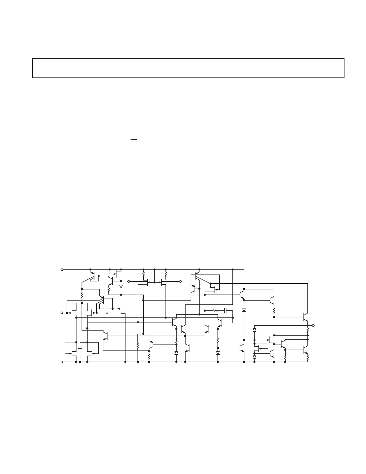
Figure 1. Simplified Schematic (1/2 OP215)
REV. A
Information furnished by Analog Devices is believed to be accurate and
reliable. However, no responsibility is assumed by Analog Devices for its
use, nor for any infringements of patents or other rights of third parties that
may result from its use. No license is granted by implication or otherwise
under any patent or patent rights of Analog Devices.
Q10
Q9
J6
C2
R2
7.4pF
Q3
R5
3.6
Q13
k
Q16
One Technology Way, P.O. Box 9106, Norwood, MA 02062-9106, U.S.A.
Tel: 781/329-4700 www.analog.com
Fax: 781/326-8703 © Analog Devices, Inc., 2002
Q4
Q2
R6
3.6k
Q15
NOTE
R7, R8 ARE ELECTRONICALLY ADJUSTED
ON-CHIP FOR MINIMUM OFFSET VOLTAGE
Q19
Q14
Q17
Q18
Q21
J9
Q24
J10
Q20
R13
Q23
R11
Q22
Q25
OUTPUT
R10
R12
Page 2

OP215–SPECIFICATIONS
ELECTRICAL CHARACTERISTICS
(at VS = ±15 V, TA = 25C, unless otherwise noted.)
OP215E OP215G
Parameter Symbol Conditions Min Type Max Min Type Max Unit
Input Offset Voltage V
OS
RS = 50 W 0.2 1.0 2.0 4.0 mV
‘G’ Grade 2.5 6.0 mV
Input Offset Current
1
I
OS
Tj = 25∞C3503100 pA
Device Operating 5 100 5 200 pA
Input Bias Current
1
I
B
Tj = 25∞C ± 15 ± 100 ± 15 ± 300 pA
Device Operating ± 18 ± 300 ± 18 ±600 pA
Input Resistance R
Large-Signal Voltage A
IN
VO
1,2
10
RL ⱖ 2 kW, 150 500 50 200 V/mV
10
1,2
W
Gain VO = ± 10 V
Output Voltage Swing V
O
RL = 10 kW±12 ± 13 ± 12 ± 13 V
RL = 2 kW±11 ± 12.7 ± 11 ± 12.7 V
Supply Current I
SY
6.0 8.5 7.0 10.0 mA
‘G’ Grade 7.0 12.0 mA
Slew Rate SR A
Gain Bandwidth GBW 3.5 5.7 3.0 5.4 MHz
Product
3
Closed-Loop Bandwidth CLBW A
Setting Time t
S
= 1 10 18 5 15 V/s
VCL
= 1 13 12 MHz
VCL
To 0.01% 2.3 2.4 s
To 0.05%
2
1.1 1.2 s
To 0.10% 0.9 1.0 s
Input Voltage Range IVR 10.2 14.8 10.1 14.8 V
–10.2 –11.5 –10.1 –11.5 V
Common-Mode CMRR V
= ± IVR 82 100 80 96 dB
CM
Rejection Ratio E, G Grades
Power Supply Rejection PSRR V
= ± 10 V to ± 16 V 10 51 V/V
S
Ratio VS = ± 10 V to ± 15 V 16 100 V/V
Input Noise Voltage nf
= 100 Hz 20 20 nV/÷Hz
O
Density fO = 1,000 Hz 15 15 nV/÷Hz
Input Noise Current I
n
fO = 100 Hz 0.01 0.01 pA/÷Hz
Density fO = 1,000 Hz 0.01 0.01 pA/÷Hz
Input Capacitance C
NOTES
1
Input bias current is specified for two different conditions. The Tj = 25∞C specification is with the junction at ambient temperature; the device operating specification is
with the device operating in a warmed up condition at 25∞ C ambient. The warmed up bias-current value is correlated to the junction temperature value via the curves
of IS versus Tj and IS versus TA. PMI has a bias-current compensation circuit that gives improved bias current and bias current over temperature versus standard
JFET input op amps. IS and IOS are measured at VCM = 0.
2
Setting time is defined here for a unity gain inverter connection using 2 kW resistors. It is the time required for the error voltage (the voltage at the inverting input pin
on the amplifier) to settle to within a specified percent of its final value from the time a 10 V step input is applied to the inverter. See setting time test circuit.
3
Sample tested.
Specifications are subject to change without notice.
IN
33pF
–2–
REV. A
Page 3

OP215
SPECIFICATIONS
(at VS = ±15 V, 0C ⱕ TA ⱕ 70C for E Grade, –40C ⱕ TA ⱕ +85C for G Grade, unless
ELECTRICAL CHARACTERISTICS
Parameter Symbol Conditions Min Type Max Min Type Max Unit
Input Offset Voltage V
Average Input Offset
Voltage Drift
Without External Trim
With External Trim TCV
Input Offset Current
Input Bias Current
2
Input Voltage Range IVR 10.2 14.7 10.1 14.7 V
Common-Mode CMRR V
Rejection Ratio
Power Supply Rejection PSRR V
Ratio VS = ± 10 V to ± 15 V 20 159 V/V
Large-Signal A
Voltage Gain VO = ± 10 V
Output Voltage Swing V
NOTES
1
Sample tested.
2
Input bias current is specified for two different conditions. The Tj = 25∞C specification is with the junction at ambient temperature; the Device Operating specification is
with the device operating in a warmed up condition at 25∞ C ambient. The warmed up bias-current value is correlated to the junction temperature value via the curves
of IS versus Tj and IS versus TA. PMI has a bias-current compensation circuit that gives improved bias current and bias current over temperature versus standard
JFET input op amps. IS and IOS are measured at VCM = 0.
Specifications are subject to change without notice.
OS
1
TCV
OS
OSn
2
I
OS
I
S
VO
O
otherwise noted.)
OP215E OP215G
RS = 50 W 0.4 1.65 3.5 8.0 mV
315 6 V/∞C
RP = 100 kW 34V/∞C
Tj = 70∞C 0.06 0.45 0.08 0.65 nA
= 70∞C 0.08 0.80 0.10 1.2 nA
T
A
Device Operating
Tj = 70∞C ± 0.12 ± 0.70 ± 0.14 ± 0.9 nA
T
= 70∞C ± 0.16 ± 1.40 ± 0.19 ± 1.8 nA
A
Device Operating
–10.2 –11.4 –10.1 –11.3 V
= ± IVR 80 98 7694 dB
CM
= ± 10 V to ± 16 V 13 100
S
RL ⱖ 2 kW 50 180 35 130 V/mV
RL ⱖ 10 kW±12 ± 13 ± 12 ± 13 V
REV. A
–3–
Page 4

OP215
WARNING!
ESD SENSITIVE DEVICE
ABSOLUTE MAXIMUM RATINGS
1
Supply Voltage
OP215E, OP215G . . . . . . . . . . . . . . . . . . . . . . . . . . . ± 18 V
Operating Temperature Range
OP215E . . . . . . . . . . . . . . . . . . . . . . . . . . . . +0∞C to +70∞C
OP215G . . . . . . . . . . . . . . . . . . . . . . . . . . . –40∞C to +85∞C
Maximum Junction Temperature (T
) . . . . . . . . . . . . . . 150∞C
j
Differential Input Voltage
OP215E . . . . . . . . . . . . . . . . . . . . . . . . . . . . . . . . . . . . ±40 V
OP215G . . . . . . . . . . . . . . . . . . . . . . . . . . . . . . . . . . . ± 30 V
Input Voltage
2
OP215E . . . . . . . . . . . . . . . . . . . . . . . . . . . . . . . . . . . . ±20 V
OP215G . . . . . . . . . . . . . . . . . . . . . . . . . . . . . . . . . . . ± 16 V
Output Short-Circuit Duration . . . . . . . . . . . . . . . . Indefinite
Storage Temperature Range . . . . . . . . . . . . –65∞C to +150∞C
Lead Temperature (Soldering, 60 sec) . . . . . . . . . . . . . 300∞C
Junction Temperature (T
NOTES
1
Absolute maximum ratings apply to packaged parts, unless otherwise noted.
2
Unless otherwise specified, the absolute maximum negative input voltage is equal
to one volt more positive than the negative power supply voltage.
) . . . . . . . . . . . . . –65∞C to +150∞C
j
ORDERING INFORMATION
Package Temperature TA = 25∞C,
Model Type Range VOS Max (mV)
OP215EZ
OP215GP
2
8-Lead CerDIP COM 1.0
2
8-Lead Plastic DIP XIND 6.0
Package Type
*
JA
JC
Unit
8-Lead Hermetic DIP (Z) 134 12 ∞C/W
8-Lead Plastic DIP (P) 96 37 ∞C/W
*JA is specified for worst-case mounting conditions, i.e., JA is specified for
device in socket for CerDIP and P-DIP packages.
PIN CONFIGURATION
OUT A
1
–IN A
+IN A
V–
1
AB
2
–
+–+
3
4
8
7
6
5
V+
OUT B
–IN B
+IN B
For military processed devices, please refer to the standard microcircuit drawing
(SMD) available at www.dscc.dla.mil/programs/milspec/default.asp
SMD Part Number ADI Equivalent
5962-8853801GA
5962-8853801PA OP215AZMDA
5962-8838032A
NOTES
1
Burn-in is available on commercial and industrial temperature range parts in CerDIP and plastic
DIP packages.
2
Not for new design, obsolete April 2002.
2
2
OP215AJMDA
OP215BRCMDA
CAUTION
ESD (electrostatic discharge) sensitive device. Electrostatic charges as high as 4000 V readily
accumulate on the human body and test equipment and can discharge without detection. Although
the OP215 features proprietary ESD protection circuitry, permanent damage may occur on devices
subjected to high-energy electrostatic discharges. Therefore, proper ESD precautions are
recommended to avoid performance degradation or loss of functionality.
–4–
REV. A
Page 5

Typical Performance Characteristics–OP215
10
V
= 15V
S
T
500ns
100
90
100
90
100ns
= 25C
A
A
= –1
V
5
10mV 5mV 1mV
0
10
0%
5V
TPC 1. Large-Signal Transient
Response
18
16
14
12
10
8
6
4
2
GAIN – dB
0
–2
–4
VS = 15V
–6
T
–8
–10
1M
= 25C
A
PHASE MARGIN = 66
AV > 10
AV = 1
10M 100M
FREQUENCY – Hz
TPC 4. Closed-Loop Bandwidth and
Phase Shift vs. Frequency
90
100
110
120
130
140
150
160
170
180
190
PHASE SHIFT – Degrees
200
10
0%
20mV
TPC 2. Small-Signal Transient
Response
28
VS = 15V
24
BANDWIDTH VARIATION FROM
< 20V IS < 5%
5 < V
20
16
12
BANDWIDTH – MHz
8
4
0
–50
S
CLOSED-LOOP
BANDWIDTH A
GAIN BANDWIDTH
PRODUCT
–25 0 25 50 75 100 125
TEMPERATURE – C
= 1
V
TPC 5. Bandwidth vs. Temperature
10mV 5mV 1mV
–5
OUTPUT VOLTAGE SWING FROM 0V – V
–10
0.5 1.0 1.5 2.0 2.5
0
SETTLING TIME – s
TPC 3. Settling Time
120
100
80
60
40
20
OPEN-LOOP VOLTAGE GAIN – dB
0
-20
10 100 1k 10k 100k 1M
1
FREQUENCY – Hz
VS = 15V
T
= 25C
A
TPC 6. Open-Loop Frequency
Response
10M
100M
28
24
20
16
12
8
PEAK-TO-PEAK AMPLITUDE – V
4
0
100K
1M 10M
FREQUENCY– Hz
VS = 15V
T
= 25C
A
A
= 1
V
TPC 7. Maximum Output Swing vs.
Frequency
REV. A
70
AV = 1
V
= 15V
S
60
50
40
30
SLEW RATE – V/s
20
10
0
–50
POSITIVE
–25 0 25 50 75 100
AMBIENT TEMPERATURE – C
NEGATIVE
125
TPC 8. Slew Rate vs. Temperature
–5–
100
80
60
40
20
COMMON-MODE REJECTION RATIO – dB
0
1
10 100 1k 10k 100k 1M 10M 100M
FREQUENCY– Hz
VS = 15V
T
= 25C
A
TPC 9. Common-Mode Rejection
Ratio vs. Frequency
Page 6

OP215
T
120
110
100
90
80
NEGATIVE
70
SUPPLY
60
50
40
30
20
POWER SUPPLY REJECTION – dB
10
0
10
100 1k 10k 100k 1M 10M
FREQUENCY – Hz
TA = 25C
POSITIVE
SUPPLY
TPC 10. Power Supply Rejection vs.
Frequency
BASIC CONNECTIONS
2k 0.1%
10V
0
+15V
–15V
SCOPE
2k 0.1%
5k
0.1%
SUMMING
MODE
2
3
2k
8
OP215
A
4
5k 0.1%
2N4416
Figure 2. Settling Time Test Circuit
100
VS = 15V
= 25C
T
A
AV = 100
10
AV = 10
1
OUTPUT IMPEDANCE –
AV = 1
0.1
10k 100k 1M 10M
1k
FREQUENCY – Hz
TPC 11. Output Impedance vs.
Frequency
V+
1
100pF
3k
A
V
= –1
2N4416
V
OUT
+15V
–IN
+IN
NOTE
V
CAN BE TRIMMED WITH POTENTIOMETERS RANGING FROM
OS
10 k TO 1 M. FOR MOST UNITS TCV
V
IS ADJUSTED WITH A 100k POTENTIOMETER.
OS
140
VS = 15V
T
= 25C
120
S
100
80
60
40
20
VOLTA GE NOISE DENSITY – nV/ Hz
0
10 100 1k 10k
1
FREQUENCY – Hz
1/f CORNER
FREQUENCY
TPC 12. Voltage Noise Density vs.
Frequency
Rp
100k
OP215
A
V–
OS
OUT A
WILL BE MINIMUM WHEN
Figure 4. Input Offset Voltage Nulling
–5V
+15V
+5V
0V
V
IN
2
8
OP215
A
3
4
2k 100pF
–15V
Figure 3. Slew Rate Test Circuit
1
V
OU
–6–
REV. A
Page 7

OP215
,
APPLICATIONS INFORMATION
Dynamic Operating Considerations
As with most amplifiers, care should be taken with lead dress,
component placement, and supply de-coupling in order to ensure
stability. For example, resistors from the output to an input should
be placed with the body close to the input to minimize “pick up”
and maximize the frequency of the feedback pole by minimizing
the capacitance from the input to ground.
A feedback pole is created when the feedback around any amplifier
is resistive. The parallel resistance and capacitance from the
input of the device (usually the inverting input) to ac ground
sets the frequency of the pole. In many instances, the frequency
of this pole is much greater than the expected 3 dB frequency of
the closed-loop gain and, consequently, there is negligible effect
on stability margin. However, if the feedback pole is less than
approximately six times the expected 3 dB frequency, a lead
capacitor should be placed from the output to the negative input
of the op amp. The value of the added capacitor should be such
that the RC time constant of this capacitor and the resistance it
parallels is greater than, or equal to, the original feedback pole
time constant.
BASIC CONNECTIONS
100k
200
100k
NOTES
1. T
A
2. RESISTORS ARE TYPE
RN55D
Figure 5. Burn-In Circuit
6
OP215
5
2
OP215
3
= 125C TO 150C
1%
+15V
B
A
–15V
8
7
1
4
PIN 1
0.200 (5.08)
MAX
0.200 (5.08)
0.125 (3.18)
0.005 (0.13)
MIN
85
1
0.100 (2.54) BSC
0.405 (10.29) MAX
0.023 (0.58)
0.014 (0.36)
8-Lead CERDIP
(Z-Suffix)
0.055 (1.4)
MAX
0.310 (7.87)
0.220 (5.59)
4
0.060 (1.52)
0.015 (0.38)
0.150
(3.81)
MIN
0.070 (1.78)
0.030 (0.76)
SEATING
PLANE
0.320 (8.13)
0.290 (7.37)
15°
0°
OUTLINE DIMENSIONS
Dimensions shown in inches and (mm).
PIN 1
0.210
(5.33)
MAX
0.160 (4.06)
0.115 (2.93)
0.015 (0.38)
0.008 (0.20)
0.022 (0.558)
0.014 (0.356)
8-Lead Plastic DIP
(P-Suffix)
0.430 (10.92)
0.348 (8.84)
8
0.100 (2.54)
1
BSC
5
0.280 (7.11)
0.240 (6.10)
4
0.070 (1.77)
0.045 (1.15)
0.060 (1.52)
0.015 (0.38)
0.130
(3.30)
MIN
SEATING
PLANE
0.325 (8.25)
0.300 (7.62)
0.015 (0.381)
0.008 (0.204)
0.195 (4.95)
0.115 (2.93)
REV. A
–7–
Page 8

OP215
Revision History
Location Page
Data Sheet changed from REV. 0 to REV. A.
Edits to GENERAL DESCRIPTION . . . . . . . . . . . . . . . . . . . . . . . . . . . . . . . . . . . . . . . . . . . . . . . . . . . . . . . . . . . . . . . . . . . . . . . . 1
Edits to ELECTRICAL CHARACTERISTICS . . . . . . . . . . . . . . . . . . . . . . . . . . . . . . . . . . . . . . . . . . . . . . . . . . . . . . . . . . . . . . 2, 3
Edits to ORDERING INFORMATION . . . . . . . . . . . . . . . . . . . . . . . . . . . . . . . . . . . . . . . . . . . . . . . . . . . . . . . . . . . . . . . . . . . . . . 4
Edits to PIN CONNECTIONS . . . . . . . . . . . . . . . . . . . . . . . . . . . . . . . . . . . . . . . . . . . . . . . . . . . . . . . . . . . . . . . . . . . . . . . . . . . . . 4
Edits to ABSOLUTE MAXIMUM RATINGS . . . . . . . . . . . . . . . . . . . . . . . . . . . . . . . . . . . . . . . . . . . . . . . . . . . . . . . . . . . . . . . . . 4
Edits to PACKAGE TYPE . . . . . . . . . . . . . . . . . . . . . . . . . . . . . . . . . . . . . . . . . . . . . . . . . . . . . . . . . . . . . . . . . . . . . . . . . . . . . . . . 4
Deleted WAFER TEST LIMITS . . . . . . . . . . . . . . . . . . . . . . . . . . . . . . . . . . . . . . . . . . . . . . . . . . . . . . . . . . . . . . . . . . . . . . . . . . . 4
Deleted DICE CHARACTERISTICS . . . . . . . . . . . . . . . . . . . . . . . . . . . . . . . . . . . . . . . . . . . . . . . . . . . . . . . . . . . . . . . . . . . . . . . 4
Deleted TYPICAL ELECTRICAL CHARACTERISTICS . . . . . . . . . . . . . . . . . . . . . . . . . . . . . . . . . . . . . . . . . . . . . . . . . . . . . . . 4
Edits to BURN-IN CIRCUIT figure . . . . . . . . . . . . . . . . . . . . . . . . . . . . . . . . . . . . . . . . . . . . . . . . . . . . . . . . . . . . . . . . . . . . . . . . . 7
C02683–0–4/02(A)
–8–
PRINTED IN U.S.A.
REV. A
 Loading...