

Page 1
www.BDTIC.com/ADI
5 MHz Single-Supply
FEATURES
Single supply: 3 V to 36 V
Wide bandwidth: 5 MHz
Low offset voltage: 1 mV
High slew rate: 10 V/μs
Low noise: 10 nV/√Hz
Unity gain stable
Input and output range includes GND
No phase reversal
APPLICATIONS
Multimedia
Telecom
ADC buffers
Wide band filters
Microphone preamplifiers
GENERAL DESCRIPTION
Operational Amplifier
OP183
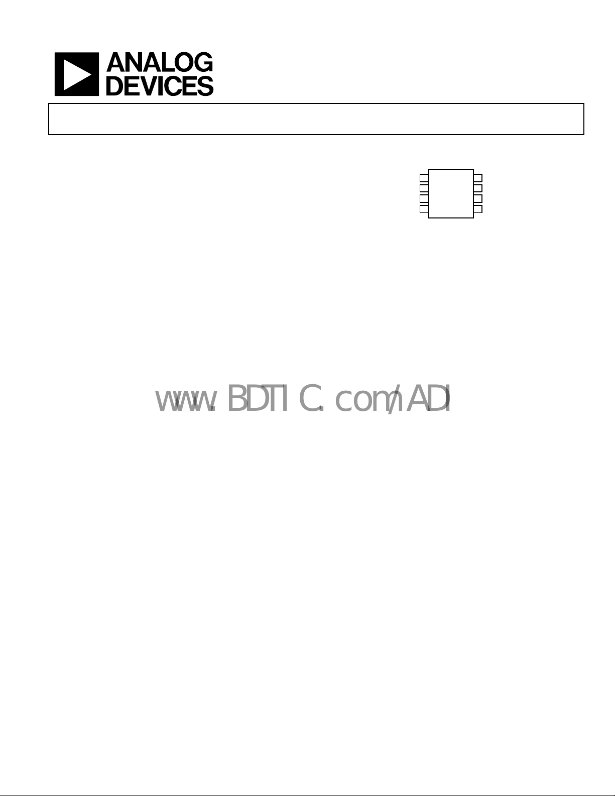
PIN CONNECTION
1
NULL
–IN
+IN
Figure 1. 8-Lead Narrow Body SOIC
V–
OP183
2
3
TOP VIEW
(Not to Scale)
4
(S Suffix)
8
NC
7
V+
6
OUT
5
NULL
00292-001
The OP183 is a single-supply, 5 MHz bandwidth amplifier with
slew rates of 10 V/μs. It can operate from voltages as low as 3 V
and up to 36 V. This combination of slew rate and bandwidth
yields excellent single-supply ac performance, making this
amplifier ideally suited for telecom and multimedia audio
applications.
The OP183 also provides good dc performance with guaranteed
1 mV o
ffset. Noise is a respectable 10 nV/√Hz. Supply current is
only 1.2 mA per amplifier.
This amplifier is well suited for single-supply applications that
equire moderate bandwidth even when used in high gain
r
configurations. This makes it useful in filters and instrumentation. The output drive capability and very wide full-power
bandwidth of the OP183 make it a good choice for multimedia
headphone drivers or microphone input amplifiers.
The OP183 is available in a SO-8 surface-mount package. It is
sp
ecified over the extended industrial (−40°C to +85°C)
temperature range.
Rev. D
Information furnished by Analog Devices is believed to be accurate and reliable.
However, no responsibility is assumed by Analog Devices for its use, nor for any
infringements of patents or other rights of third parties that may result from its use.
Specifications subject to change without notice. No license is granted by implication
or otherwise under any patent or patent rights of Analog Devices. Trademarks and
registered trademarks are the property of their respective owners.
One Technology Way, P.O. Box 9106, Norwood, MA 02062-9106, U.S.A.
Tel: 781.329.4700 www.analog.com
Fax: 781.461.3113 ©2005 Analog Devices, Inc. All rights reserved.
Page 2

OP183
www.BDTIC.com/ADI
TABLE OF CONTENTS
Specifications..................................................................................... 3
Direct Access Arrangement...................................................... 13
Electrical Characteristics @ V
Electrical Characteristics @ V
Electrical Characteristics @ V
Absolute Maximum Ratings............................................................ 6
ESD Caution.................................................................................. 6
Typical Performance Characteristics .............................................7
Applications..................................................................................... 13
Offset Adjust ...............................................................................13
Phase Reversal............................................................................. 13
= 5 V......................................... 3
S
= 3 V......................................... 4
S
= ±15 V.................................... 5
S
REVISION HISTORY
5/05—Rev. C to Rev. D
Updated Format.................................................................. Universal
Removed OP283 .................................................................Universal
Updated Outline Dimensions........................................................16
Changes to Ordering Guide...........................................................16
5 V Only Stereo DAC for Multimedia..................................... 13
Low Voltage Headphone Amplifiers........................................ 14
Low Noise Microphone Amplifier for Multimedia ............... 14
3 V 50 Hz/60 Hz Active Notch Filter with False Ground .....14
Low Voltage Frequency Synthesizer for Wireless
Transceiver ..................................................................................15
Outline Dimensions....................................................................... 16
Ordering Guide .......................................................................... 16
Revision 0: Initial Version
2/02—Rev. B to Rev. C
dits to FEATURES...........................................................................1
E
Edits to GENERAL DESCRIPTION...............................................1
Edits to SPECIFICATIONS......................................................... 2–3
Edits to Package Type........................................................................4
Edits to ORDERING GUIDE...........................................................4
Edits to ABSOLUTE MAXIMUM RATINGS ...............................4
Edits to OUTLINE DIMENSIONS...............................................12
Rev. D | Page 2 of 16
Page 3
OP183
www.BDTIC.com/ADI
SPECIFICATIONS
ELECTRICAL CHARACTERISTICS @ VS = 5 V
TA = 25°C, unless otherwise noted.
Table 1.
Parameter Symbol Conditions Min Typ Max Unit
INPUT CHARACTERISTICS
Offset Voltage VOS V
−40°C ≤ TA ≤ +85°C 1.25 mV
Input Bias Current IB V
−40°C ≤ TA ≤ +85°C 430 750 nA
Input Offset Current IOS V
−40°C ≤ TA ≤ +85°C 11 ±50 nA
Input Voltage Range 0 3.5 V
Common-Mode Rejection Ratio CMRR VCM = 0 to 3.5 V
Large Signal Voltage Gain AVO R
Offset Voltage Drift ΔVOS/ΔT 4 μV/°C
Bias Current Drift ΔIB/ΔT −1.6 nA/°C
OUTPUT CHARACTERISTICS
Output Voltage High VOH R
Output Voltage Low VOL R
Short-Circuit Limit ISC Source 25 mA
Sink 30 mA
POWER SUPPLY
Power Supply Rejection Ratio PSRR VS = 4 V to 6 V,
Supply Current/Amplifier ISY V
Supply Voltage Range VS
DYNAMIC PERFORMANCE
Slew Rate SR RL = 2 kΩ 5 10
Full Power Bandwidth BWp 1% Distortion
Settling Time tS To 0.01%
Gain Bandwidth Product GBP
Phase Margin фm
NOISE PERFORMANCE
Voltage Noise en p-p 0.1 Hz to 10 Hz
Voltage Noise Density en f = 1 kHz, VCM = 2.5 V
Current Noise Density in
= 2.5 V, V
CM
= 2.5 V, V
CM
= 2.5 V, V
CM
−40°C ≤ TA ≤ +85°C
= 2 kΩ, 0.2 ≤ VO ≤ 3.8 V 100 V/mV
L
= 2 kΩ to GND 4.0 4.22 V
L
= 2 kΩ to GND 50 75 mV
L
= 2.5 V, 0.025 1.0 mV
OUT
= 2.5 V, 350 600 nA
OUT
= 2.5 V, nA
OUT
70 104 dB
−40°C ≤ T
= 2.5 V,
O
−40°C ≤ T
≤ +85°C 70 104
A
≤ +85°C
A
3
1.2 1.5 mA
>50
1.5
5
46
2
10
0.4
dB
±18 V
V/μs
kHz
μs
MHz
Degrees
μV p-p
nV/√Hz
pA/√Hz
Rev. D | Page 3 of 16
Page 4
OP183
www.BDTIC.com/ADI
ELECTRICAL CHARACTERISTICS @ VS = 3 V
TA = 25°C, unless otherwise noted.
Table 2.
Parameter Symbol Conditions Min Typ Max Unit
INPUT CHARACTERISTICS
Offset Voltage VOS V
Input Bias Current IB V
Input Offset Current IOS V
Input Voltage Range
Common-Mode Rejection Ratio CMRR VCM = 0 V to 1.5 V,
Large Signal Voltage Gain AVO R
OUTPUT CHARACTERISTICS
Output Voltage High VOH R
Output Voltage Low VOL R
Short-Circuit Limit ISC Source
POWER SUPPLY
Power Supply Rejection Ratio PSRR VS = 2.5 V to 3.5 V,
Supply Current/Amplifier ISY −40°C ≤ TA ≤ +85°C, VO = 1.5 V
DYNAMIC PERFORMANCE
Gain Bandwidth Product GBP
NOISE PERFORMANCE
Voltage Noise Density en f = 1 kHz, VCM = 1.5 V
= 1.5 V, V
CM
−40°C ≤ T
= 1.5 V, V
CM
−40°C ≤ T
= 1.5 V, V
CM
−40°C ≤ T
= 1.5 V,
OUT
≤ +85°C
A
= 1.5 V,
OUT
≤ +85°C
A
= 1.5 V,
OUT
≤ +85°C
A
0.3 1.0 mV
1.25 mV
350 600 nA
750 nA
0
11 ±50 nA
1.5 V
nA
−40°C ≤ T
= 2 kΩ, 0.2 ≤ VO ≤ 1.8 V 100 260
L
≤ +85°C 70 103
A
dB
V/mV
= 2 kΩ to GND 2.0 2.25
L
= 2 kΩ to GND
L
Sink
90 125 mV
25
30
V
mA
mA
−40°C ≤ T
≤ +85°C 60 113
A
1.2 1.5 mA
dB
5
MHz
10
nV/√Hz
Rev. D | Page 4 of 16
Page 5
OP183
www.BDTIC.com/ADI
ELECTRICAL CHARACTERISTICS @ VS = ±15 V
TA = 25°C, unless otherwise noted.
Table 3.
Parameter Symbol Conditions Min Typ Max Unit
INPUT CHARACTERISTICS
Offset Voltage VOS
Input Bias Current IB
Input Offset Current IOS −40 ≤ TA ≤ +85°C
Input Voltage Range
Common-Mode Rejection Ratio CMRR VCM = −15 V to +13.5 V,
Large Signal Voltage Gain AVO R
Offset Voltage Drift ΔVOS/ΔT
Bias Current Drift ΔIB/ΔT
Long-Term Offset Voltage VOS Note
OUTPUT CHARACTERISTICS
Output Voltage High VOH
Output Voltage Low VOL
Short-Circuit Limit ISC Source
Open-Loop Output Impedance Z
POWER SUPPLY
Power Supply Rejection Ratio PSRR VS = ± 2.5 V to ± 18 V,
Supply Current/Amplifier ISY V
Supply Voltage Range VS
DYNAMIC PERFORMANCE
Slew Rate SR RL = 2 kΩ 10 15
Full Power Bandwidth BWp 1% Distortion
Settling Time tS To 0.01%
Gain Bandwidth Product GBP
Phase Margin фm
NOISE PERFORMANCE
Voltage Noise en p-p 0.1 Hz to 10 Hz
Voltage Noise Density en f = 1 kHz
Current Noise Density in
1
Long-term offset voltage is guaranteed by a 1,000 hour life test performed on three independent lots at 125°C, with an LTPD of 1.3.
−40°C ≤ T
A
−40°C ≤ T
A
≤ +85°C
≤ +85°C
−15
0.01 1.0 mV
1.25 mV
300 600 nA
400 750 nA
11 ±50 nA
+13.5 V
–40°C ≤ TA ≤ +85°C 70 86
= 2 kΩ 100 1000
L
1
3
−1.6
1.5 mV
dB
V/mV
μV/°C
nA/°C
RL = 2 kΩ to GND, −40°C ≤ TA ≤ +85°C
RL = 2 kΩ to GND, −40°C ≤ TA ≤ +85°C
Sink
f = 1 MHz, AV = +1
OUT
13.9 14.1
−14.05 −13.9 V
30
50
15
V
mA
mA
Ω
−40°C ≤ T
= ±18 V, VO = 0 V,
S
−40°C ≤ T
≤ +85°C 70 112
A
≤ +85°C
A
3
1.2 1.75 mA
dB
±18 V
50
1.5
5
56
V/μs
kHz
μs
MHz
Degrees
2
10
0.4
μV p-p
nV/√Hz
pA/√Hz
Rev. D | Page 5 of 16
Page 6

OP183
www.BDTIC.com/ADI
ABSOLUTE MAXIMUM RATINGS
Table 4.
Parameter Rating
Supply Voltage ±18 V
Input Voltage ±18 V
Differential Input Voltage
Output Short-Circuit Duration to GND Indefinite
Storage Temperature Range
S Package −65°C to +150°C
Operating Temperature Range
OP183 −40°C to +85°C
Junction Temperature Range
S Package −65°C to +150°C
Lead Temperature Range (Soldering 60 sec) 300°C
1
For supply voltages less than ±7 V, the absolute maximum input voltage is
equal to the supply voltage. Maximum input current should not exceed
2 mA.
1
±7 V
ESD CAUTION
ESD (electrostatic discharge) sensitive device. Electrostatic charges as high as 4000 V readily accumulate on
the human body and test equipment and can discharge without detection. Although this product features
proprietary ESD protection circuitry, permanent damage may occur on devices subjected to high energy
electrostatic discharges. Therefore, proper ESD precautions are recommended to avoid performance
degradation or loss of functionality.
Stresses above those listed under Absolute Maximum Ratings
y cause permanent damage to the device. This is a stress
ma
rating only; functional operation of the device at these or any
other conditions above those indicated in the operational
section of this specification is not implied. Exposure to absolute
maximum rating conditions for extended periods may affect
device reliability.
Absolute maximum ratings apply to packaged parts, unless
herwise noted.
ot
Table 5.
Package Type θ
8-Lead SOIC (S) 158 43 °C/W
1
θJA is specified for worst-case conditions; in other words, θJA is specified for
device soldered in circuit board for SOIC packages.
1
θ
JA
JC
Units
Rev. D | Page 6 of 16
Page 7

OP183
www.BDTIC.com/ADI
TYPICAL PERFORMANCE CHARACTERISTICS
80
70
60
50
40
QUANTITY
30
20
VS = 5V
300X
OP AMPS
160
140
120
100
80
60
QUANTITY (Amplifiers)
40
–40°C = TA +85°C
300X OP AMPS
PLASTIC PACKAGE
10
0
–600 –400 –200 0 200 400 600
INPUT OFFSET VOLTAGE (μV)
Figure 2. OP183 Input Offset Voltage Distribution @ 5 V
80
70
60
50
40
QUANTITY
30
20
10
0
–600 –400 –200 0 200 400 600
INPUT OFFSET VOLTAGE (μV)
VS = 5V
300X
OP AMPS
Figure 3. OP183 Input Offset Voltage Distribution @ ±15 V
160
140
120
100
80
60
QUANTITY (Amplifiers)
40
20
0
02468101
TCV
OS
Figure 4. OP183 Input Offset Voltage Drift (TCV
–40°C = TA +85°C
300X OP AMPS
PLASTIC PACKAGE
(μV/°C)
) Distribution @ 5 V
OS
00292-002
00292-003
00292-004
2
20
0
02468101
Figure 5. OP183 Input Offset Voltage Drift (TCV
3
2
1
MAXIMUM OUTPUT SWING (V p-p)
0
1k 10k 100k 1M 10M
TCV
(μV/°C)
OS
FREQUENCY (Hz)
) Distribution @ ±15 V
OS
TA = 25°C
R
L
V
S
Figure 6. OP183 Maximum Output Swing vs. Frequency @ 3 V
5
4
3
2
1
MAXIMUM OUTPUT SWING (V p-p)
0
1k 10k 100k 1M 10M
FREQUENCY (Hz)
TA = 25°C
R
L
V
S
Figure 7. OP183 Maximum Output Swing vs. Frequency @ 5 V
= 2kΩ
= 3V
= 2kΩ
= 5V
00292-005
2
00292-006
00292-007
Rev. D | Page 7 of 16
Page 8

OP183
www.BDTIC.com/ADI
30
25
TA = 25°C
R
= 2kΩ
L
V
= 15V
S
500
400
VS = ±15V,
V
= +5V
S
20
15
10
MAXIMUM OUTPUT SWING (V p-p)
5
0
1k 10k 100k 1M 10M
FREQUENCY (Hz)
Figure 8. OP183 Maximum Output Swing vs. Frequency @ ±15 V
1
SINK
100m
10m
OUTPUT VOLTAGEΔ TO RAIL (V)
SOURCE
00292-008
300
200
INPUT BIAS CURRENT (nA)
100
0
–75 –50 –25 0 25 50 75
VS = +3V
TEMPERATURE (°C)
Figure 11. Input Bias Current vs. Temperature
1.50
VS = ±18V
R
=
∞
1.25
1.00
0.75
0.50
0.25
SUPPLY CURRENT AMPLIFIER (mA)
L
VS = +3V
R
=
∞
L
VS = +5V
R
=
L
100 125
00292-011
∞
1m
1μ 10μ 100μ 1m 10m
LOAD CURRENT (A)
Figure 9. Output Voltage vs. Sink & Source Current
600
TA = 25°C
V
= ±15V
500
400
300
200
INPUT BIAS CURRENT (nA)
100
0
–15 –10 –5 0 5 10 13.5
COMMON MODE VOLTAGE (V)
S
Figure 10. Input Bias Current vs. Common-Mode Voltage
00292-009
00292-010
0
–75 –50 –25 0 25 50 75
TEMPERATURE (°C)
Figure 12. Supply Current per Amplifier vs. Temperature
1.50
TA = 25°C
1.25
1.00
0.75
0.50
0.25
SUPPLY CURRENT AMPLIFIER (mA)
0
0 ±2.5 ±5.0 ±7.5 ±10.0 ±12.5 ±15.0
SUPPLY VOLTAGE (V)
Figure 13. Supply Current per Amplifier vs. Supply Voltage
100 125
±17.5 ±20.0
00292-012
00292-013
Rev. D | Page 8 of 16
Page 9

OP183
www.BDTIC.com/ADI
60
50
40
30
20
SHORT-CIRCUIT CURRENT (mA)
10
–1
SC
+1
SC
140
120
100
80
60
40
COMMON-MODE REJECTION (dB)
20
+PSRR
–PSRR
TA = 25°C
V
= ±15V
S
0
–75 –50 –25 0 25 50 75
TEMPERATURE (°C)
100 125
Figure 14. Short-Circuit Current vs. Temperature @ 5 V
60
–1
50
40
30
20
SHORT-CIRCUIT CURRENT (mA)
10
0
–75 –50 –25 0 25 50 75
SC
+1
SC
TEMPERATURE (°C)
100 125
Figure 15. Short-Circuit Current vs. Temperature @ ±15 V
140
120
100
80
60
40
COMMON-MODE REJECTION (dB)
20
0
100 1k 10k 100k 1M
FREQUENCY (Hz)
TA = 25°C
V
S
Figure 16. Commo n-Mode Re jection v s. Frequency
= ±15V
00292-014
00292-015
00292-016
0
100 1k 10k 100k 1M
FREQUENCY (Hz)
Figure 17. Power Supply Rejection vs. Frequency
90
80
70
60
50
40
GAIN (dB)
30
20
10
0
–10
1k 10k 100k 1M 10M
GAIN
PHASE
FREQUENCY (Hz)
TA = 25°C
V
= 3V
S
R
= 10kΩ
L
PHASE
MARGIN
= 43°
Figure 18. Open-Loop Gain and Phase vs. Frequency @ 3 V
90
80
70
60
50
40
GAIN (dB)
30
20
10
0
–10
1k 10k 100k 1M 10M
GAIN
PHASE
FREQUENCY (Hz)
TA = 25°C
V
= 5V
S
R
= 10kΩ
L
PHASE
MARGIN
= 46°
Figure 19. Open-Loop Gain and Phase vs. Frequency @ 5 V
195
90
45
0
–45
195
90
45
0
–45
00292-017
PHASE (Degrees)
00292-018
PHASE (Degrees)
00292-019
Rev. D | Page 9 of 16
Page 10

OP183
www.BDTIC.com/ADI
90
80
70
60
50
40
GAIN (dB)
30
20
10
0
–10
1k 10k 100k 1M 10M
Figure 20. Open-Loop Gain and Phase vs. Frequency @ ±15 V
GAIN
PHASE
FREQUENCY (Hz)
TA = 25°C
V
= ±15V
S
R
= 10kΩ
L
PHASE
MARGIN
= 56°
195
90
45
0
–45
PHASE (Degrees)
00292-020
25
20
s)
μ
15
10
SLEW RATE (V/
5
0
–75 –50 –25 0 25 50 75
VS = ±15V
R
= 2kΩ
L
±SLEW RATE
VS = ±15V
R
= 2kΩ
L
±SLEW RATE
TEMPERATURE (°C)
Figure 23. Slew Rate vs. Temperature
100 125
00292-023
1000
900
800
700
600
500
400
300
OPEN-LOOP GAIN (V/mV)
200
100
0
–75 –50 –25 0 25 50 75
VS = ±15V
OR
V
= +3V
S
R
= 2kΩ
L
VS = +5V
R
= 2kΩ
L
TEMPERATURE (°C)
Figure 21. Open-Loop Gain vs. Temperature
50
AV = 100
AV = 10
AV = 1
CLOSED-LOOP GAIN (dB)
–10
40
30
20
10
0
100 125
TA = 25°C
V
= ±15V
S
00292-021
30
25
Hz)
√
20
15
10
5
VOLTAGE NOISE DENSITY (nA
0
10 100 1k 10k
FREQUENCY (Hz)
TA = +25°C
V
= ±15V
S
OR
V
= +3V, +15V
S
Figure 24. Voltage Noise Density vs. Frequency
Hz)
√
CURRENT NOISE DENSITY (pA
6
5
4
3
2
1
TA = 25°C
V
= ±15V
S
OR
V
= +3V, +15V
S
00292-024
–20
1k 10k 100k 1M 10M
FREQUENCY (Hz)
00292-022
Figure 22. Closed-Loop Gain vs. Frequency
Rev. D | Page 10 of 16
0
10 100 1k 10k
FREQUENCY (Hz)
Figure 25. Current Noise Density vs. Frequency
00292-025
Page 11

OP183
www.BDTIC.com/ADI
100
90
80
70
)
Ω
60
50
40
IMPEDANCE (
30
20
10
0
100 1k 10k 100k 1M
FREQUENCY (Hz)
Figure 26. Closed-Loop Output Impedance vs. Frequency
80
TA = 25°C
70
V
= 5V
S
R
= 10kΩ
L
60
TA = 25°C
V
AV = 10
= ±15V
S
AV = 1
00292-026
Figure 29. Small Signal Performance @ ±15 V
00292-029
50
40
30
20
SMALL SIGNAL OVERSHOOT (%)
10
0
0 100 200 300
NEGATIVE
EDGE
CAPACITANCE (pF)
POSITIVE
EDGE
Figure 27. Small Signal Overshoot vs. Load Capacitance
Figure 28. Large Signal Performance @ ±15 V
00292-027
00292-028
00292-030
Figure 30. 0.1 Hz to 10 Hz Noise @ ±2.5 V
00292-031
Figure 31. 0.1 Hz to 10 Hz Noise @ ±15 V
Rev. D | Page 11 of 16
Page 12

OP183 Preliminary Technical Data
www.BDTIC.com/ADI
0.1
OP183
V
=±2.5V
S
A
= +1
V
R
= 0
F
V
= 1V
IN
80kHz LOW-PASS FILTER
0.010
RMS
600
Ω
1k
Ω
2k
Ω
5k
Ω
DISTORTION (%)
10
0.001
0.0005
20 100 1k 10k 20k
FREQUENCY (Hz)
Figure 32. THD + Noise vs. Frequency for Various Loads
Ω
NO
LOAD
00292-032
Rev. D | Page 12 of 16
Page 13

OP183
2
www.BDTIC.com/ADI
APPLICATIONS
OFFSET ADJUST
Figure 33 shows how the offset voltage of the OP183 can be
adjusted by connecting a potentiometer between Pins 1 and 5,
and connecting the wiper to V
the potentiometer is 10 kΩ. This will give an adjustment range
of approximately ±1 mV. If a larger adjustment span is desired, a
50 kΩ potentiometer will yield a range of ±2.5 mV.
3
OP183
2
. The recommended value for
EE
V
CC
7
6
4
5
V
1
EE
V
OS
This arrangement drives the transformer differentially so that
he drive to the transformer is effectively doubled over a single
t
amplifier arrangement. This application takes advantage of the
ability of the OP183 to drive capacitive loads and to save power
in single-supply applications.
300pF
37.4kΩ
20kΩ
20kΩ
A2
475Ω
RxA
0.1μF
A1
0.0047μF
OP183
3.3kΩ
OP183
00292-033
Figure 33. OP183 Offset Adjust
PHASE REVERSAL
The OP183 is protected against phase reversal as long as both of
the inputs are within the range of the positive supply and the
negative supply −0.6 V. If there is a possibility of either input
going beyond these limits, however, the inputs should be
protected with a series resistor to limit input current to 2 mA.
DIRECT ACCESS ARRANGEMENT
The OP183 can be used in a single supply direct access
arrangement (DAA) as shown in Figure 34. This figure shows a
ortion of a typical DAA capable of operating from a single 5 V
p
supply; with minor modifications it should also work on 3 V
supplies. Amplifiers A2 and A3 are configured so that the
transmit signal TxA is inverted by A2 and not inverted by A3.
AD1868
V
1
L
16-BIT
LL
2
DL
3
CK
4
DR
5
LR
6 11
7 10
DGND
VBR
8 9
DAC
18-BIT
SERIAL
REG.
18-BIT
SERIAL
REG.
16-BIT
DAC
V
V
VBL
16
15
14
VOL
AGND
VOR
13
12
V
S
REF
REF
Figure 35. 5 V Only 18-Bit Stereo DAC
7.68kΩ
330pF
7.68kΩ
330pF
TxA
.5V
0.1μF
REF
20kΩ
750pF
OP183
22.1kΩ
20kΩ
20kΩ
0.33μF
A3
00292-034
Figure 34. Direct Access Arrangement
5 V ONLY STEREO DAC FOR MULTIMEDIA
The low noise and single-supply capability of the OP183 are
ideally suited for stereo DAC audio reproduction or sound
synthesis applications, such as multimedia systems. Figure 35
sho
ws an 18-bit stereo DAC output setup that is powered from a
single 5 V supply. The low noise preserves the 18-bit dynamic
range of the AD1868.
8
9.76kΩ
9.76kΩ
3
OP183
2
6
OP183
5
4
7.68kΩ
7.68kΩ
100pF
100pF
220μF
+–
1
220μF
+–
7
47kΩ
47kΩ
LEFT
CHANNEL
OUTPUT
RIGHT
CHANNEL
OUTPUT
00292-035
Rev. D | Page 13 of 16
Page 14

OP183
www.BDTIC.com/ADI
LOW VOLTAGE HEADPHONE AMPLIFIERS
Figure 36 shows a stereo headphone output amplifier for the
AD1849 16-bit SoundPort® Stereo Codec device. The
pseudoreference voltage is derived from the common-mode
voltage generated internally by the AD1849, thus providing a
convenient bias for the headphone output amplifiers.
OPTIONAL
GAIN
1kΩ
V
REF
10μF
21
LOUT1L
AD1849
CMOUT
LOUT1R
10kΩ
V
REF
19
10kΩ
20
10μF
L VOLUME
CONTROL
R VOLUME
CONTROL
1kΩ
V
Figure 36. Headphone Output Amplif
OP183
OP183
OPTIONAL
GAIN
REF
5kΩ
5V
220μF
16Ω
47kΩ
5V
OP183
220μF
16Ω
47kΩ
5kΩ
ier for Multimedia Sound Codec
HEADPHONE
LEFT
HEADPHONE
RIGHT
LOW NOISE MICROPHONE AMPLIFIER FOR MULTIMEDIA
The OP183 is ideally suited as a low noise microphone preamp
for low voltage audio applications. Figure 37 shows a gain of 100
tereo preamp for the AD1849 16-bit SoundPort Stereo Codec
s
chip. The common-mode output buffer serves as a phantom
power driver for the microphones.
10kΩ
5V
17
19
18
MINL
AD1849
CMOUT
MINR
00292-037
20Ω
20Ω
10μF
10μF
5V
1/2
OP219
50Ω
10kΩ
100Ω
10kΩ
50Ω
LEFT
ELECTRET
CONDENSER
MIC
INPUT
RIGHT
ELECTRET
CONDENSER
MIC
INPUT
Figure 37. Low Noise Stereo Microphone Amplifier for
Multimedia Sound Codec
OP183
100Ω
OP183
10kΩ
00292-036
3 V 50 HZ/60 HZ ACTIVE NOTCH FILTER WITH FALSE GROUND
To process ac signals, it may be easier to use a false-ground bias
rather than the negative supply as a reference ground. This
would reject the power line frequency interference which can
often obscure low frequency physiological signals, such as heart
rates, blood pressures, EEGs, and ECGs.
Figure 38 shows a 50 Hz/60 Hz active notch filter for
liminating line noise in patient monitoring equipment. It has
e
several kilohertz bandwidth and is not sensitive to false-ground
perturbations. The simple false-ground circuit shown achieves
good rejection of low frequency interference using standard offthe-shelf components.
R2
2.67kΩ
R1
A1
3V
R10
25kΩ
2.67kΩ3VC1
4
1
5
3
A3
4
2.67kΩ
(1μF × 2)
0.015μF
OP183
1μF
R3
1μF
C5
V
IN
10kΩ
2
3
R6
OP183
R9
75kΩ
C4
1μF
Figure 38. 3 V Supply 50 Hz/60 Hz Notch Filter with Pseudo Ground
Amplifier A3 biases A1 and A2 to the middle of their input
common-mode range. When operating on a 3 V supply, the
center of the common-mode range of the OP183 is 0.75 V. This
notch filter effectively squelches 60 Hz pickup at a filter Q of
0.75. To reject 50 Hz interference, change the resistors in the
twin-T section (R1 through R5) from 2.67 kΩ to 3.16 kΩ.
The filter section uses OP183 op amps in a twin-T
co
nfiguration whose frequency selectivity is very sensitive to
the relative matching of the capacitors and resistors in the twinT section. Mylar is the material of choice for the capacitors, and
the relative matching of the capacitors and resistors determines
the filter’s pass-band symmetry. Using 1% resistors and 5%
capacitors produces satisfactory results.
C3
10kΩ
R11
1
C2
1μF
R4
2.67kΩ
R5
1.33kΩ
(2.67kΩ÷ 2)
R12
70Ω
0.75V
OP183
6
A2
8
R7
1kΩ
R8
1kΩ
Q = 0.75
NOTE:
FOR 50Hz APPLICATIONS
CHANGE R1–R4 TO 3.1Ω
AND R5 TO 1.58Ω (3.16Ω÷ 2).
C6
1μF
7
V
O
00292-038
Rev. D | Page 14 of 16
Page 15

OP183
www.BDTIC.com/ADI
LOW VOLTAGE FREQUENCY SYNTHESIZER FOR
WIRELESS TRANSCEIVER
The low noise and low voltage operation capability of the
OP183 serves well for the loop filter of a frequency synthesizer.
CRYSTAL
REFERENCE
OSCILLATOR
PHASE
DETECTOR
3V
OP183
Figure 39 shows a typical application in a radio transceiver. The
ph
ase noise performance of the synthesizer depends on low
noise contribution from each component in the loop as the
noise is amplified by the frequency division factor of the
prescaler.
The resistors used in the low-pass filter should be of low to
oderate values to reduce noise contribution due to the input
m
bias current as well as the resistors themselves. The filter cutoff
frequency should be chosen to optimize the loop constant.
QB4
BA
QB2
RB2 RB1
QB5A
JB1
QB3
QB1
QB9
CB1
R10
R3LT
RB3
2
1
R3AT
R1 R2
Q1 Q2
R3A
R3B
Z1
CC1
QB10
R4A
R4B
R11
R4AT
R4LT
Figure 39. Low Voltage Frequency Synthesizer for a Wireless Transceiver
RB4 RB5 RB6
QB6
3
5
QB7
QD1
Q3 Q4
QB12
PRESCALER
Q7 Q8
QB8
Q5
CF1 R5
QB13
QB14
Q6
V
÷
CC3
Q10
RF
OUT
QB11
QD2
R9
CC2
QD3
CO
R7
CONTROL
VCO
900MHz
R8
7
Q12
Q11
00292-039
6
Figure 40. OP183 Simplified Schematic
Rev. D | Page 15 of 16
4
00292-040
Page 16

OP183
www.BDTIC.com/ADI
OUTLINE DIMENSIONS
5.00 (0.1968)
4.80 (0.1890)
4.00 (0.1574)
3.80 (0.1497)
85
6.20 (0.2440)
5.80 (0.2284)
41
1.27 (0.0500)
BSC
0.25 (0.0098)
0.10 (0.0040)
COPLANARITY
0.10
CONTROLLING DIMENSIONS ARE IN MILLIMETERS; INCH DIMENSIONS
(IN PARENTHESES) ARE ROUNDED-OFF MILLIMETER EQUIVALENTS FOR
REFERENCE ONLY AND ARE NOT APPROPRIATE FOR USE IN DESIGN
SEATING
PLANE
COMPLIANT TO JEDEC STANDARDS MS-012-AA
1.75 (0.0688)
1.35 (0.0532)
0.51 (0.0201)
0.31 (0.0122)
0.25 (0.0098)
0.17 (0.0067)
0.50 (0.0196)
0.25 (0.0099)
8°
1.27 (0.0500)
0°
0.40 (0.0157)
× 45°
Figure 41. 8-Lead Standard Small Outline Package [SOIC_N]
Nar
row Body
(R-8)
S-Suffix
Dimensions shown in millimeters and (inches)
ORDERING GUIDE
Model Temperature Range Package Description Package Option
OP183GS −40°C to +85°C 8-Lead SOIC_N S-Suffix (R-8)
OP183GS-REEL −40°C to +85°C 8-Lead SOIC_N S-Suffix (R-8)
OP183GS-REEL7 −40°C to +85°C 8-Lead SOIC_N S-Suffix (R-8)
OP183GSZ
OP183GSZ-REEL1 −40°C to +85°C 8-Lead SOIC_N S-Suffix (R-8)
OP183GSZ-REEL71 −40°C to +85°C 8-Lead SOIC_N S-Suffix (R-8)
1
Z = Pb free part.
1
−40°C to +85°C 8-Lead SOIC_N S-Suffix (R-8)
©2005 Analog Devices, Inc. All rights reserved. Trademarks and
registered trademarks are the property of their respective owners.
C00292-0-5/05(D)
Rev. D | Page 16 of 16
 Loading...