

Page 1
5 MHz Single-Supply
1
2
3
4
8
7
6
5
TOP VIEW
(Not to Scale)
OP183
NULL
–IN
+IN
V–
NC = NO CONNECT
NC
V+
OUT
NULL
1
2
3
4
8
7
6
5
OP183
1
2
3
4
8
7
6
5
TOP VIEW
(Not to Scale)
OP283
OUTA
–INA
+INA
V–
V+
OUTB
–INB
+INB
1
2
3
4
8
7
6
5
OP283
a
FEATURES
Single-Supply – +3 Volts to +36 Volts
Wide Bandwidth – 5 MHz
Low Offset Voltage – <1 mV
High Slew Rate – 10 V/ms
Low Noise – 10 nV/√
Unity-Gain Stable
Input and Output Range Includes GND
No Phase Reversal
APPLICATIONS
Multimedia
Telecom
ADC Buffers
Wide Band Filters
Microphone Preamplifiers
GENERAL DESCRIPTION
The OP183 is a single-supply, 5 MHz bandwidth amplifier with
slew rates of 10 V/µs. The OP283 is a dual version. Both can
operate from voltages as low as 3 volts and up to 36 volts. This
combination of slew rate and bandwidth yields excellent singlesupply ac performance making them ideally suited for telecom and
multimedia audio applications.
Hz
Operational Amplifiers
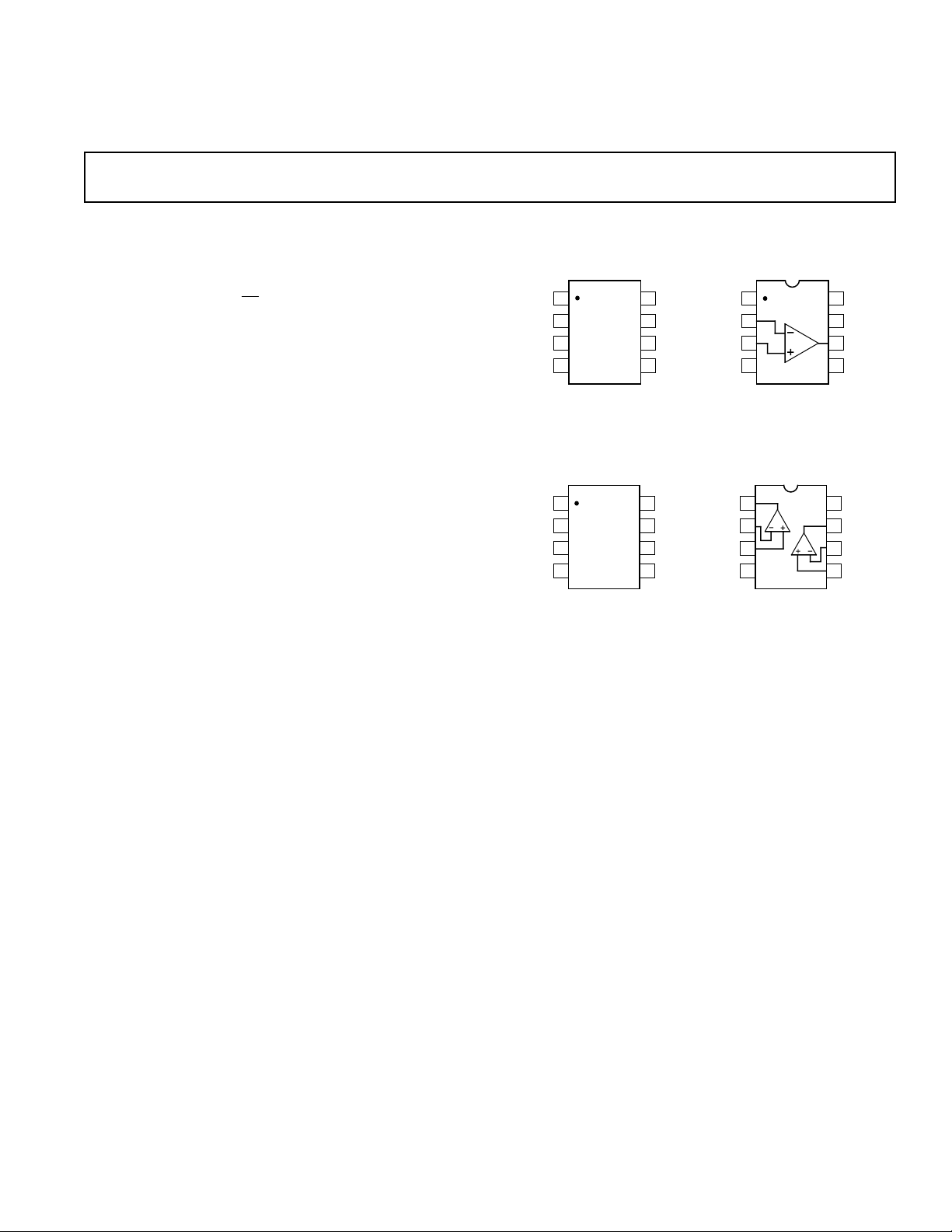
PIN CONNECTIONS
8-Lead Narrow-Body SO
(S Suffix)
8-Lead Narrow-Body SO
(S Suffix)
OP183/OP283
8-Lead Epoxy DIP
(P Suffix)
8-Lead Epoxy DIP
(P Suffix)
In addition to its ac characteristics, the OP183 family provides
good dc performance with guaranteed 1 mV offset. Noise is a
respectable 10 nV/√Hz. Supply current is only 1.2 mA per amplifier.
These amplifiers are well suited for single-supply applications that
require moderate bandwidths even when used in high gain configurations. This makes them useful in filters and instrumentation.
Their output drive capability and very wide full power bandwidth
make them a good choice for multimedia headphone drivers or
microphone input amplifiers.
The OP183 and OP283 are available in 8-pin plastic DIP and SO-8
surface mount packages. They are specified over the extended
industrial (–40°C to +85°C) temperature range.
REV. B
Information furnished by Analog Devices is believed to be accurate and
reliable. However, no responsibility is assumed by Analog Devices for its
use, nor for any infringements of patents or other rights of third parties
which may result from its use. No license is granted by implication or
otherwise under any patent or patent rights of Analog Devices.
One Technology Way, P.O. Box 9106, Norwood. MA 02062-9106, U.S.A.
Tel: 617/329-4700 Fax: 617/326-8703
Page 2

OP183/OP283–SPECIFICA TIONS
ELECTRICAL CHARACTERISTICS
(@ VS = +5.0 V, TA = +258C unless otherwise noted)
Parameter Symbol Conditions Min Typ Max Units
INPUT CHARACTERISTICS
Offset Voltage V
Input Bias Current I
Input Offset Current I
OS
B
OS
VCM = 2.5 V, V
–40°C ≤ TA ≤ +85°C 1.25 mV
VCM = 2.5 V, V
–40°C ≤ TA ≤ +85°C 430 750 nA
VCM = 2.5 V, V
–40°C ≤ TA ≤ +85°C11±50 nA
= 2.5 V, 0.025 1.0 mV
OUT
= 2.5 V, 350 600 nA
OUT
= 2.5 V, nA
OUT
Input Voltage Range 0 +3.5 V
Common-Mode Rejection Ratio CMRR VCM = 0 to 3.5 V
–40°C ≤ TA ≤ +85°C 70 104 dB
Large Signal Voltage Gain A
Offset Voltage Drift ∆VOS/∆T4µV/°C
VO
RL = 2 kΩ, 0.2 ≤ VO ≤ 3.8 V 100 V/mV
Bias Current Drift ∆IB/∆T –1.6 nA/°C
OUTPUT CHARACTERISTICS
Output Voltage High V
Output Voltage Low V
Short Circuit Limit I
OH
OL
SC
RL = 2 kΩ to GND +4.0 4.22 V
RL = 2 kΩ to GND 50 75 mV
Source 25 mA
Sink 30 mA
POWER SUPPLY
Power Supply Rejection Ratio PSRR VS = +4 V to +6 V,
–40°C ≤ TA ≤ +85°C 70 104 dB
Supply Current/Amplifier I
Supply Voltage Range V
SY
S
VO = 2.5 V,
–40°C ≤ TA ≤ +85°C 1.2 1.5 mA
+3 ±18 V
DYNAMIC PERFORMANCE
Slew Rate SR RL = 2 kΩ 510 V/µs
Full-Power Bandwidth BWp 1% Distortion >50 kHz
Settling Time t
Gain Bandwidth Product GBP 5 MHz
S
To 0.01% 1.5 µs
Phase Margin φm 46 Degrees
NOISE PERFORMANCE
Voltage Noise en
Voltage Noise Density e
Current Noise Density i
p-p
n
n
0.1 Hz to 10 Hz 2 µV p-p
f = 1 kHz, VCM = 2.5 V 10 nV/√Hz
0.4 pA/√Hz
ELECTRICAL CHARACTERISTICS
(@ VS = +3.0 V, TA = +258C unless otherwise noted)
Parameter Symbol Conditions Min Typ Max Units
INPUT CHARACTERISTICS
Offset Voltage V
Input Bias Current I
Input Offset Current I
OS
B
OS
VCM = 1.5 V, V
–40°C ≤ TA ≤ +85°C 1.25 mV
VCM = 1.5 V, V
–40°C ≤ TA ≤ +85°C 750 nA
VCM = 1.5 V, V
–40°C ≤ TA ≤ +85°C11±50 nA
= 1.5 V, 0.3 1.0 mV
OUT
= 1.5 V, 350 600 nA
OUT
= 1.5 V, nA
OUT
Input Voltage Range 0 +1.5 V
Common-Mode Rejection Ratio CMRR VCM = 0 V to 1.5 V,
–40°C ≤ TA ≤ +85°C 70 103 dB
Large Signal Voltage Gain A
VO
RL = 2 kΩ, 0.2 ≤ VO ≤ 1.8 V 100 260 V/mV
OUTPUT CHARACTERISTICS
Output Voltage High V
Output Voltage Low V
Short Circuit Limit I
OH
OL
SC
RL = 2 kΩ to GND +2.0 2.25 V
RL = 2 kΩ to GND 90 125 mV
Source 25 mA
Sink 30 mA
POWER SUPPLY
Power Supply Rejection Ratio PSRR VS = +2.5 V to +3.5 V,
–40°C ≤ TA ≤ +85°C 60 113 dB
Supply Current/Amplifier I
SY
–40°C ≤ TA ≤ +85°C, VO = 1.5 V 1.2 1.5 mA
DYNAMIC PERFORMANCE
Gain Bandwidth Product GBP 5 MHz
NOISE PERFORMANCE
Voltage Noise Density e
n
f = 1 kHz, VCM = 1.5 V 10 nV/√Hz
–2–
REV. B
Page 3

OP183/OP283
ELECTRICAL CHARACTERISTICS
(@ VS = 615.0 V, TA = +258C unless otherwise noted)
Parameter Symbol Conditions Min Typ Max Units
INPUT CHARACTERISTICS
Offset Voltage V
Input Bias Current I
Input Offset Current I
OS
–40°C ≤ T
B
–40°C ≤ T
OS
–40 ≤ TA ≤ +85°C11±50 nA
≤ +85°C 1.25 mV
A
≤ +85°C 400 750 nA
A
0.01 1.0 mV
300 600 nA
Input Voltage Range –15 +13.5 V
Common-Mode Rejection Ratio CMRR VCM = –15 V to +13.5 V,
≤ +85°C7086dB
A
Large Signal Voltage Gain A
Offset Voltage Drift ∆V
Bias Current Drift ∆I
Long Term Offset Voltage V
–40°C ≤ T
VO
/∆T3µV/°C
OS
/∆T –1.6 nA/°C
B
OS
RL = 2 kΩ 100 1000 V/mV
Note 1 1.5 mV
OUTPUT CHARACTERISTICS
Output Voltage High V
Output Voltage Low V
Short-Circuit Limit I
OH
OL
SC
RL = 2 kΩ to GND, –40°C ≤ TA ≤ +85°C +13.9 14.1 V
RL = 2 kΩ to GND, –40°C ≤ TA ≤ +85°C –14.05 –13.9 V
Source 30 mA
Sink 50 mA
Open -Loop Output Impedance Z
OUT
f = 1 MHz, AV = +1 15 Ω
POWER SUPPLY
Power Supply Rejection Ratio PSRR VS = ±2.5 V to ±18 V,
Supply Current/Amplifier I
Supply Voltage Range V
–40°C ≤ T
SY
VS = ±18 V, VO = 0 V,
–40°C ≤ T
S
≤ +85°C 70 112 dB
A
≤ +85°C 1.2 1.75 mA
A
+3 ±18 V
DYNAMIC PERFORMANCE
Slew Rate SR RL = 2 kΩ 10 15 V/µs
Full-Power Bandwidth BW
Settling Time t
S
p
1% Distortion 50 kHz
To 0.01% 1.5 µs
Gain Bandwidth Product GBP 5 MHz
Phase Margin φm 56 degrees
NOISE PERFORMANCE
Voltage Noise e
Voltage Noise Density e
Current Noise Density i
NOTES
1
Long term offset voltage is guaranteed by a 1000 hour life test performed on three independent lots at +125°C, with an LTPD of 1.3.
Specifications subject to change without notice.
WAFER TEST LIMITS
n p-p
n
n
(@ VS = +5.0 V, TA = +258C unless otherwise noted)
0.1 Hz to 10 Hz 2 µV p-p
f = 1 kHz 10 nV/√Hz
0.4 pA/√Hz
Parameter Symbol Conditions Limit Units
Offset Voltage V
Input Bias Current I
Input Offset Current I
OS
B
OS
Common-Mode Rejection CMRR V
VS = ±15 V, VO = 0 V 1.0 mV max
VCM = 2.5 V ±600 nA max
VCM = 2.5 V ±50 nA max
= 0 V to 3.5 V 70 dB min
CM
Power Supply Rejection Ratio PSRR V = ±2.5 V to ±18 V 70 dB min
Large Signal Voltage Gain A
Output Voltage High V
Output Voltage Low V
Supply Current/Amplifier I
NOTE
Electrical tests and wafer probe to the limits shown. Due to variations in assembly methods and normal yield loss, yield after packaging is not guaranteed for standard
product dice. Consult factory to negotiate specifications based on dice lot qualifications through sample lot assembly and testing.
VO
OH
OL
SY
REV.B
RL = 2 kΩ, 0.2 ≤ VO ≤ 3.8 V 100 V/mV min
RL = 2 kΩ 4.0 V min
RL = 2 kΩ 75 mV max
VS = ±15 V, VO = 0 V, RL = ∞ 1.5 mA max
–3–
Page 4
OP183/OP283
ABSOLUTE MAXIMUM RATINGS
1
Supply Voltage . . . . . . . . . . . . . . . . . . . . . . . . . . . . . . . . . . ±18 V
Input Voltage . . . . . . . . . . . . . . . . . . . . . . . . . . . . . . . . . . . . ±18 V
2
Differential Input Voltage
. . . . . . . . . . . . . . . . . . . . . . . . . . . ±7V
Output Short-Circuit Duration to GND . . . . . . . . . . . . Indefinite
Storage Temperature Range
P, S Package . . . . . . . . . . . . . . . . . . . . . . . . . . –65°C to +150°C
Operating Temperature Range
OP183/OP283G . . . . . . . . . . . . . . . . . . . . . . . . –40°C to +85°C
Junction Temperature Range
P, S Package . . . . . . . . . . . . . . . . . . . . . . . . . . .–65°C to +150°C
Lead Temperature Range (Soldering 60 Sec) . . . . . . . . . . +300°C
Package Type θ
3
JA
θ
JC
Units
8-Pin Plastic DIP (P) 103 43 °C/W
8-Pin SOIC (S) 158 43 °C/W
NOTES
1
Absolute maximum ratings apply to both DICE and packaged parts, unless
otherwise noted.
2
For supply voltages less than ±7 V, the absolute maximum input voltage is equal
to the supply voltage. Maximum input current should not exceed 2 mA.
3
θJA is specified for the worst case conditions, i.e., θJA is specified for device in socket
for P-DIP packages; θJA is specified for device soldered in circuit board for SOIC
packages.
ORDERING GUIDE
DICE CHARACTERISTICS
V+ OUT NULL
NULL
–IN IN+ V–
OP183 Die Size 0.058 X 0.063 Inch, 3,717 Sq. Mils
Substrate (Die Backside) Is Connected to V–.
Transistor Count, 30.
V+ OUTB –INB
+INB
Temperature Package Package
Model Range Description Option
OP183GP –40°C to +85°C 8-Pin Plastic DIP N-8
OP183GS –40°C to +85°C 8-Pin SOIC SO-8
OP283GP –40°C to +85°C 8-Pin Plastic DIP N-8
OP283GS –40°C to +85°C 8-Pin SOIC SO-8
OUTA –INA V–
+INA
OP283 Die Size 0.063 X 0.092 Inch, 5,796 Sq. Mils
Substrate (Die Backside) Is Connected to V–.
Transistor Count, 55.
–4–
REV. B
Page 5

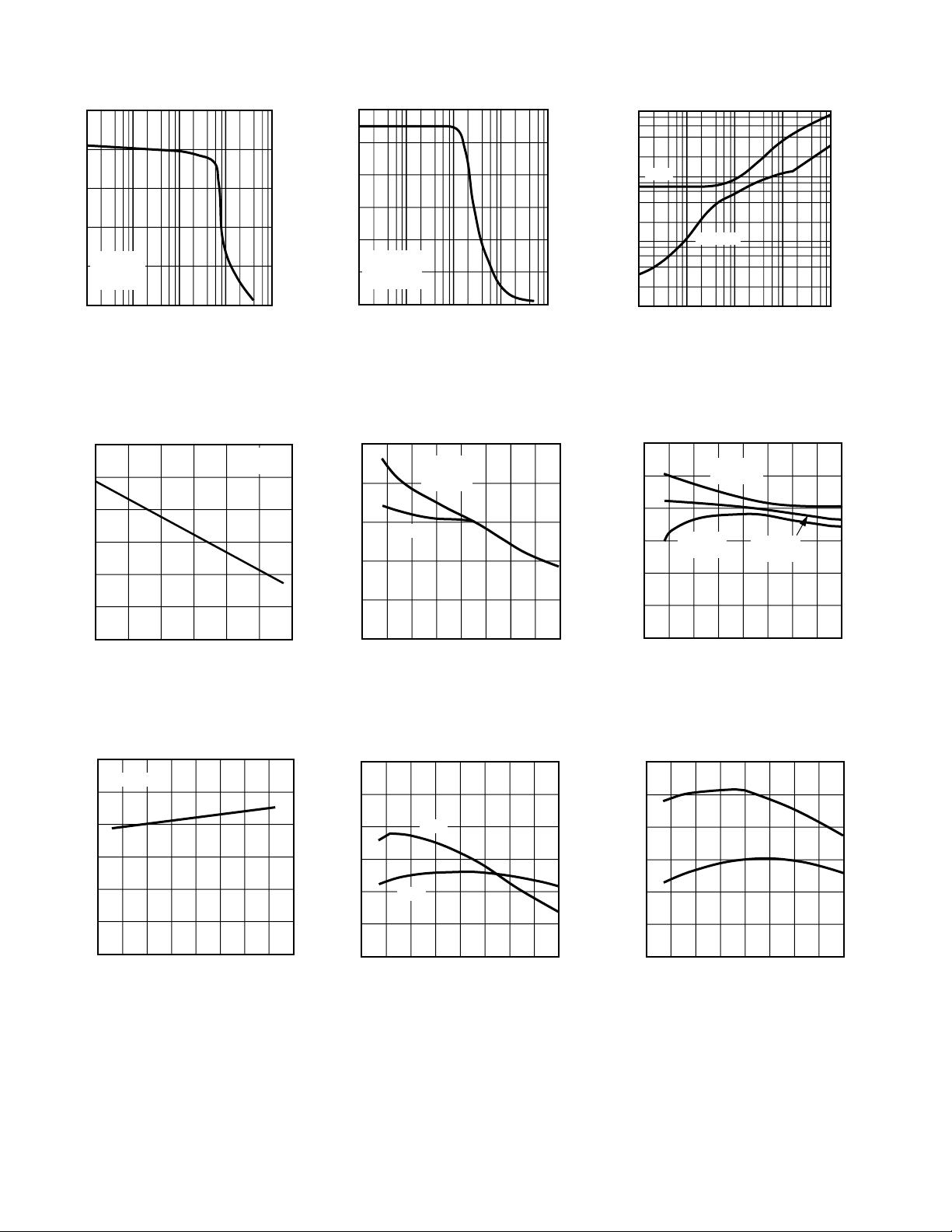
80
160
0
40
20
80
60
100
120
140
+600+400+2000–200–400–600
INPUT OFFSET VOLTAGE – µV
QUANTITY
VS = +5V
590X
OP AMPS
3
1
0
1k
10k 10M1M100k
2
FREQUENCY – Hz
MAXIMUM OUTPUT SWING – Volts
p-p
ΩTA = +25°C
R
L
= 2kΩ
V
S
= +3V
70
60
50
40
QUANTITY
30
20
10
0
VS = +5V
300X
OP AMPS
INPUT OFFSET VOLTAGE – µV
T ypical Characteristics–OP183/OP283
80
70
60
50
40
QUANTITY
30
20
10
+600 +400 +200 0–200 –400 –600
0
INPUT OFFSET VOLTAGE – µV
VS = ±15V
300X
OP AMPS
+600+400+2000–200–400–600
Figure 1. OP183 Input Offset Voltage
Distribution @ +5 V
160
140
120
100
80
QUANTITY
60
40
20
0
INPUT OFFSET VOLTAGE – µV
VS = ±15V
590X
OP AMPS
+600+400+2000–200–400–600
Figure 4. OP283 Input Offset Voltage
Distribution @ ±15 V
200
180
160
140
120
100
80
60
QUANTITY – Amplifiers
≤–40°C ≤ TA ≤ +85°C
590X OP AMPS
PLASTIC PACKAGE
Figure 2. OP183 Input Offset Voltage
Distribution @ ±15 V
160
140
120
100
80
60
QUANTITY – Amplifiers
40
20
0
20
≤–40°C ≤ TA ≤ +85°C
300X OP AMPS
PLASTIC PACKAGE
TCVOS – µV/°C
10864
12
Figure 5. OP183 Input Offset Voltage
Drift (TCVOS) Distribution @ +5 V
200
180
160
140
120
100
80
60
QUANTITY – Amplifiers
≤–40°C ≤ TA ≤ +85°C
590X OP AMPS
PLASTIC PACKAGE
Figure 3. OP283 Input Offset Voltage
Distribution @ +5 V
160
140
120
100
80
60
QUANTITY – Amplifiers
40
20
0
20
≤–40°C ≤ TA ≤ +85°C
300X OP AMPS
PLASTIC PACKAGE
TCVOS – µV/°C
12
10864
Figure 6. OP183 Input Offset Voltage
Drift (TCV
) Distribution @ ±15 V
OS
20
0
Figure 7. OP283 Input Offset Voltage
Drift (TCVOS) Distribution @ +5 V
REV.B
2400
TCVOS – µV/°C
20
0
1481046 12
16
2400
TCVOS – µV/°C
Figure 8. OP283 Input Offset Voltage
Drift (TCVOS) Distribution @ ±15 V
16
1481046 12
Figure 9. OP183/OP283 Maximum
Output Swing vs. Frequency @ +3 V
–5–
Page 6
60
0
125
30
10
–50
20
–75
50
40
1007550250–25
TEMPERATURE – °C
SHORT CIRCUIT CURRENT – mA
–I
SC
+I
SC
OP183/OP283–Typical Characteristics
5
p-p
4
3
2
ΩTA = +25°C
1
R
= 2kΩ
L
V
= +5V
S
MAXIMUM OUTPUT SWING – Volts
0
1k
10k 10M1M100k
FREQUENCY – Hz
30
p-p
25
20
15
10
ΩTA = +25°C
R
= 2kΩ
L
5
V
= ±15V
S
MAXIMUM OUTPUT SWING – Volts
0
1k
10k 10M1M100k
FREQUENCY – Hz
1
SINK
100m
10m
OUTPUT VOLTAGE ∆ TO RAIL – Volts
1m
1µ
SOURCE
10µ 10m1m100µ
LOAD CURRENT – Amps
Figure 10. OP183/OP283 Maximum
Output Swing vs. Frequency @ +5 V
600
500
400
300
200
INPUT BIAS CURRENT – nA
100
0
–10
–15
COMMON-MODE VOLTAGE – Volts
TA = +25°C
V
= ±15V
S
1050–5
13.5
Figure 13. Input Bias Current vs.
Common-Mode Voltage
1.50
TA = +25°C
1.25
Figure 11. OP183/OP283 Maximum
Output Swing vs. Frequency @ ±15 V
500
VS = ±15V
&
= +5V
400
300
200
INPUT BIAS CURRENT – nA
100
0
–75
V
VS = +3V
–50
TEMPERATURE – °C
S
1007550250–25
125
Figure 14. Input Bias Current vs.
Temperature
60
50
Figure 12. Output Voltage vs. Sink
& Source Current
1.50
∞VS = ±18V
R
=
1.25
1.00
0
–75
–50
VS = +3V
R
L
0.75
0.50
0.25
SUPPLY CURRENT\AMPLIFIER – mA
∞
L
=
∞
TEMPERATURE – °C
VS = +5V
R
=
L
∞
1007550250–25
Figure 15. Supply Current per
Amplifier vs. Temperature
125
1.00
0.75
0.50
0.25
SUPPLY CURRENT\AMPLIFIER – mA
0
±2.5
0
SUPPLY VOLTAGE – Volts
Figure 16. Supply Current per
Amplifier vs. Supply Voltage
–I
40
30
20
10
SHORT CIRCUIT CURRENT – mA
±17.5±15±12.5±10±7.5±5
±20
0
–75
–50
Figure 17. Short-Circuit Current vs.
Temperature @ +5 V
SC
+I
SC
TEMPERATURE – °C
–6–
1007550250–25
125
Figure 18. Short-Circuit Current vs.
Temperature @
±
15 V
REV. B
Page 7

140
1000
0
125
300
100
–50
200
–75
600
400
500
700
800
900
10025 50–25 0 75
TEMPERATURE – °C
OPEN-LOOP GAIN – V/mV
ΩVS = +5V
R
L
= 2kΩ
ΩVS = ±15V
OR
V
S
= +3V
R
L
= 2kΩ
10
100 10k
30
15
0
10
5
20
25
1k
FREQUENCY – Hz
VOLTAGE NOISE DENSITY – nV/ Hz
TA = +25°C
V
S
= ±15V
OR
V
S
= +3V, +15V
90
40
–10
1k
10k 10M1M100k
50
70
80
0
10
30
60
20
FREQUENCY – Hz
GAIN – dB
ΩTA = +25°C
V
S
= +3V
R
L
= 10kΩ
GAIN
PHASE
PHASE
MARGIN
= 43°
–45
0
45
90
PHASE – Degrees
135
120
TA = +25°C
V
= ±15V
S
140
120
TA = +25°C
V
= ±15V
S
OP183/OP283
100
80
60
40
20
COMMON-MODE REJECTION – dB
0
100
1k 1M100k10k
FREQUENCY – Hz
Figure 19. Common-Mode Rejection
vs. Frequency
90
80
70
60
50
40
30
GAIN – dB
20
10
0
–10
1k
GAIN
PHASE
10k 10M1M100k
FREQUENCY – Hz
ΩTA = +25°C
V
= +5V
S
= 10kΩ
R
L
PHASE
MARGIN
= 46°
100
80
60
40
20
POWER SUPPLY REJECTION – dB
0
100
–PSRR
1k 1M100k10k
FREQUENCY – Hz
Figure 20. Power Supply Rejection
vs. Frequency
90
80
70
135
90
45
0
PHASE – Degrees
–45
60
50
40
30
GAIN – dB
20
10
0
–10
1k
PHASE
GAIN
10k 10M1M100k
FREQUENCY – Hz
+PSRR
ΩTA = +25°C
V
= ±15V
S
= 10kΩ
R
L
PHASE
MARGIN
= 56°
Figure 21. Open-Loop Gain and Phase
vs. Frequency @ +3 V
135
90
45
0
PHASE – Degrees
–45
Figure 22. Open-Loop Gain and Phase
vs. Frequency @ +5 V
50
40
30
20
10
0
CLOSED-LOOP GAIN – dB
–10
–20
1k
Figure 25. Closed-Loop Gain vs.
Frequency
REV.B
10k 10M1M100k
AV = +100
AV = +10
AV = +1
FREQUENCY – Hz
TA = +25°C
V
= ±15V
S
Figure 23. Open-Loop Gain and Phase
vs. Frequency @ ±15 V
25
20
15
10
SLEW RATE – V/µs
5
0
–50
–75
ΩVS = ±15V
= 2kΩ
R
L
± SLEW RATE
ΩVS = ±5V
= 2kΩ
R
L
± SLEW RATE
TEMPERATURE – °C
1007550250–25
125
Figure 26. Slew Rate vs. Temperature
–7–
Figure 24. Open-Loop Gain vs.
Temperature
Figure 27. Voltage Noise Density
vs. Frequency
Page 8

OP183/OP283–Typical Characteristics
80
0
300
20
10
100
0
40
30
50
60
70
200
CAPACITANCE – pF
SMALL SIGNAL OVERSHOOT – %
NEGATIVE
EDGE
POSITIVE
EDGE
ΩTA = +25°C
V
S
= ±15V
R
L
= 2kΩ
90
100
10
0%
1S
5mV
6.0
5.0
4.0
3.0
2.0
1.0
CURRENT NOISE DENSITY – pA/ Hz
0
10
100 10k1k
FREQUENCY – Hz
TA = +25°C
V
S
V
S
= ±15V
OR
= +3\+5V
100
90
80
70
60
50
40
IMPEDANCE – Ω
30
20
10
0
100
1k 1M100k10k
AV = +1
FREQUENCY – Hz
TA = +25°C
V
= ±15V
S
AV = +10
Figure 28. Current Noise Density
vs. Frequency
100
90
10
0%
5V 1µS
Figure 31. Large Signal Performance
@
±
15 V
1S
100
90
Figure 29. Closed-Loop Output
Impedance vs. Frequency
100
90
10
0%
50mV 200nS
Figure 32. Small Signal Performance
@ ±15 V
OP283
V
= ±2.5V
S
= +1 RF = 0
A
V
= 1V
V
IN
RMS
80kHz LOW PASS FILTER
Figure 30. Small Signal Overshoot
vs. Load Capacitance
Figure 33. 0.1 Hz to 10 Hz Noise
@ ± 2.5 V
600Ω
1kΩ
2kΩ
5kΩ
10
0%
5mV
Figure 34. 0.1 Hz to 10 Hz Noise
±
15 V
@
DISTORTION – %
FREQUENCY – Hz
10Ω
NO LOAD
Figure 35. THD + Noise vs. Frequency for Various Loads
–8–
REV. B
Page 9

OP183/OP283
1/2 OP283
+5V
1/2 OP283
Ω5kΩ
OPTIONAL
GAIN
Ω1kΩ
V
REF
1/2 OP283
+5V
V
REF
ΩOPTIONAL
GAIN
1kΩ
Ω5kΩ
29
19
31
Ω10kΩ
10µF
LOUT1L
LOUT1R
CMOUT
AD1849
V
REF
10µF
Ω10kΩ
L VOLUME
CONTROL
R VOLUME
CONTROL
Ω16Ω
220µF
Ω47kΩ
HEADPHONE
LEFT
Ω16Ω
220µF
Ω47kΩ
HEADPHONE
RIGHT
APPLICATIONS
OP183 Offset Adjust
Figure 36 shows how the OP183’s offset voltage can be adjusted by
connecting a potentiometer between Pins 1 and 5, and connecting
the wiper to V
. The recommended value for the potentiometer is
EE
10 kΩ. This will give an adjustment range of approximately ±1 mV.
If larger adjustment span is desired, a 50 kΩ potentiometer will
yield a range of ±2.5 mV.
V
CC
7
3
OP183
2
1
6
4
5
V
EE
V
OS
Figure 36. OP183 Offset Adjust
Phase Reversal
The OP183 family is protected against phase reversal as long as
both of the inputs are within the range of the positive supply and
the negative supply minus 0.6 volts. However if there is a possibility
of either input going beyond these limits, then the inputs should be
protected with a series resistor to limit input current to 2 mA.
Direct Access Arrangement
The OP183/OP283 can be used in a single supply Direct Access
Arrangement (DAA) as is shown in Figure 37. This figure shows a
portion of a typical DAA capable of operating from a single +5 volt
supply and it should also work on +3 volt supplies with minor
modifications. Amplifiers A2 and A3 are configured so that the
transmit signal TXA is inverted by A2 and is not inverted by A3.
This arrangement drives the transformer differentially so that the
drive to the transformer is effectively doubled over a single amplifier
arrangement. This application takes advantage of the OP183/283’s
ability to drive capacitive loads, and to save power in single supply
applications.
300pF
+5 Volt Only Stereo DAC for Multimedia
The OP283’s low noise and single supply capability are ideally
suited for stereo DAC audio reproduction or sound synthesis
applications such as multimedia systems. Figure 38 shows an 18-bit
stereo DAC output setup that is powered from a single +5 volt
supply. The low noise preserves the 18-bit dynamic range of the
AD1868. For DACs that operate on dual supplies, the OP283 can
also be powered from the same supplies.
+5V SUPPLY
AD1868
V
L
1
18-BIT
DAC
2
LL
18-BIT
3
SERIAL
DL
REG.
4
CK
5
DR
18-BIT
SERIAL
6
LR
REG.
7
DGND
18-BIT
VBR
8
DAC
VBL
16
15
14
VOL
V
REF
13
AGND
12
V
REF
11
VOR
10
9
S
V
Ω7.68k
Ω
330pF
Ω7.68kΩ
330pF
Ω9.76kΩ
Ω9.76kΩ
Ω7.68kΩ
Ω7.68kΩ
6
5
8
1/2 OP283
432
1/2 OP283
100pF
100pF
220µF
220µF
Ω47kΩ
Ω47kΩ
LEFT
CHANNEL
OUTPUT
RIGHT
CHANNEL
OUTPUT
1
7
Figure 38. +5 Volt Only 18-Bit Stereo DAC
Low Voltage Headphone Amplifiers
Figure 39 shows a stereo headphone output amplifier for the
AD1849 16-bit SoundPort
Stereo Codec device. The pseudoreference voltage is derived from the common-mode voltage
generated internally by the AD1849, thus providing a convenient
bias for the headphone output amplifiers.
0.0047µF
Ω37.4kΩ
A1
Ω3.3kΩ
OP283
A2
Ω20kΩ
Ω20kΩ
Ω475Ω
RXA
0.1µF
OP283
0.1µF
REV.B
TXA
Ω20kΩ
2.5V
REF
Figure 37. Direct Access Arrangement
Ω22.1kΩ
Ω20kΩ
OP283
750pF
Ω20kΩ
A3
0.33µF
Figure 39. Headphone Output Amplifier for Multimedia
Sound Codec
SoundPort is a registered trademark of Analog Devices Inc.
–9–
Page 10

OP183/OP283
Low Noise Microphone Amplifier for Multimedia
The OP183 family is ideally suited as a low noise microphone
preamp for low voltage audio applications. Figure 40 shows a gain
of 100 stereo preamp for the AD1849 16-bit SoundPort Stereo
Codec chip. The common-mode output buffer serves as a “phantom power” driver for the microphones.
Ω10kΩ
+5V
LEFT
ELECTRET
CONDENSER
MIC
INPUT
RIGHT
ELECTRET
CONDENSER
MIC
INPUT
Ω20Ω
Ω20Ω
10µF
+5V
1/2 OP213
10µF
Ω50Ω
Ω50Ω
Ω10kΩ
Ω10kΩ
1/2 OP283
Ω100Ω
Ω100Ω
1/2 OP283
Ω10kΩ
17
MINL
AD1849
CMOUT
19
MINR
15
bandwidth and is not sensitive to false-ground perturbations. The
simple false-ground circuit shown achieves good rejection of low
frequency interference using standard off-the-shelf components.
Amplifier A3 biases A1 and A2 to the middle of their input
common-mode range. When operating on a +3 V supply, the
center of the OP283’s common-mode range is 0.75 V. This notch
filter effectively squelches 60 Hz pickup at a filter Q of 0.75. To
reject 50 Hz interference, simply change the resistors in the twin-T
section (R1 through R5) from 2.67 kΩ to 3.16 kΩ.
The filter section uses an OP283 dual op amp in a twin-T configuration whose frequency selectivity is very sensitive to the relative
matching of the capacitors and resistors in the twin-T section.
Mylar is the material of choice for the capacitors, and the relative
matching of the capacitors and resistors determines the filter’s pass
band symmetry. Using 1% resistors and 5% capacitors produces
satisfactory results.
A Low Voltage Frequency Synthesizer for Wireless
Transceiver
The OP183’s low noise and the low voltage operation capability
serves well for the loop filter of a frequency synthesizer. Figure 42
shows a typical application in a radio transceiver. The phase noise
performance of the synthesizer depends on low noise contribution
from each component in the loop as the noise is amplified by the
frequency division factor of the prescaler.
Figure 40. Low Noise Stereo Microphone Amplifier for
Multimedia Sound CODEC
A +3 Volt 50 Hz/60 Hz Active Notch Filter with False Ground
To process ac signals, it may be easier to use a false-ground bias
rather than the negative supply as a reference ground. This would
reject the power-line frequency interference which oftentimes can
obscure low frequency physiological signals, such as heart rates,
blood pressures, EEGs, ECGs, et cetera.
Ω
R2
2.67kΩ
+3V
ΩR1
2.67kΩ
2
8
A1
V
IN
ΩR6
10kΩ
ΩR9
75kΩ
C4
1µF
4
3
1/2 OP283
+3V
2
3
ΩR10
25kΩ
A1, A2, AND A3 = 1/2 OP283
1
(1µF × 2)
C5
0.015µF
A3
OP183
ΩR3
2.67kΩ
×C3
2µF
ΩR11
10kΩ
1
1µF
C1
ΩR12
70Ω
C2
1µF
ΩR4
2.67kΩ
Ω
R5
1.33kΩ
(2.67kΩ ÷ 2)
0.75V
C6
1µF
1/2 OP283
5
A2
6
ΩR8
1kΩ
Ω
Q = 0.75
NOTE: FOR 50Hz APPLICATIONS
CHANGE R1–R4 TO 3.1k Ω
AND R5 TO 1.58k Ω (3.16kΩ ÷ 2).
ΩR7
1kΩ
V
7
O
CONTROL
VCO
900MHz
+3V
OP183
VARACTER
DIODE
CRYSTAL
REFERENCE
OSCILLATOR
PHASE
DETECTOR
÷
PRESCALER
RF
OUT
V
Figure 42. A Low Voltage Frequency Synthesizer for a
Wireless Transceiver
The resistors used in the low-pass filter should be of low to
moderate values to reduce noise contribution due to the input bias
current as well as the resistors themselves. The filter cutoff
frequency should be chosen to optimize the loop constant.
Figure 41. +3 Volt Supply 50 Hz/60 Hz Notch Filter with
Pseudo Ground
Figure 41 shows a 50 Hz/60 Hz active notch filter for eliminating
line noise in patient monitoring equipment. It has several kilohertz
–10–
REV. B
Page 11

OP183/OP283
7
QB9
RB3
R1
Q1
CB1
R10
R3LT
2
1
R3A
R3AT
R3B
JB1
QB5A
QB4
B
A
QB2
RB1
RB2
QB3
QB1
CC1
QB10
R2
Q2
Z1
R4A
R11
R4AT
R4B
R4LT
RB4
3
5
Figure 43. OP183 Simplified Schematic
* OP283 SPICE Macro-model Rev. A, 9/93
* JCB/ADI
*
* Copyright 1993 by Analog Devices
*
* Refer to “README.DOC” file for License Statement.
* Use of this model indicates your acceptance of the terms and
* provisions in the License Statement.
*
* Node assignments
* noninverting input
* | inverting input
* | | positive supply
* | | | negative supply
* | | | | output
* ||| | |
.SUBCKT OP283 2 1 99 50 45
*
* INPUT STAGE AND POLE AT 600 kHz
*
I1 99 8 1E-4
Q1 416 QP
Q2 537 QP
CIN 1 2 1.5PF
R1 50 4 1591
R2 50 5 1591
C1 4 5 83.4E-12
R3 6 8 1075
R4 7 8 1075
IOS 1 2 12.5E-9
EOS 3 2 POLY(1) (15,98) 25E-6 1
DC1 2 36 DZ
DC2 1 36 DZ
*
* GAIN STAGE AND DOMINANT POLE AT 10 Hz
*
EREF 98 0 POLY(2) (99,0) (50,0) 0 0.5 0.5
RB5
Q7
QB7QB6
Q5
QD1
Q3
QB13
QB12
RB6
Q8
QB8
Q6
CF1
Q4
R5
QB14
CC3
QB11
R9
QD2
QD3
Q10
CC2
R7
Q12
R8
CO
Q11
4
G1 98 9 (4,5) 6.28E-4
R5 9 98 1.59E9
C2 9 98 10E-12
D1 9 10 DX
D2 11 9 DX
E1 10 98 POLY(1) 99 98 -1.35 1.03
V2 50 11 –0.63
*
* COMMON MODE STAGE WITH ZERO AT 353 Hz
*
ECM 14 98 POLY(2) (1,98) (2,98) 0 3.5 3.5
R7 14 15 1E6
C4 14 15 3.75E-11
R8 15 98 1
*
*POLE AT 20 MHz
*
GP2 98 31 (9,98) 1E-6
RP2 31 98 1E6
CP2 31 98 7.96E-15
*
*ZERO AT 1.5 MHz
*
EZ1 32 98 (31,98) 1E6
RZ1 32 33 1E6
RZ2 33 98 1
CZ1 32 33 106E-15
*
*POLE AT 10 MHz
*
GP10 98 40 (33,98) 1E-6
RP10 40 98 1E6
CP10 40 98 15.9E-15
*
* OUTPUT STAGE
*
RO1 99 45 140
6
REV.B
–11–
Page 12

OP183/OP283
RO2 45 50 140
G7 45 99 (99,40) 7.14E-3
G8 50 45 (40,50) 7.14E-3
G9 98 60 (45,40) 7.14E-3
D7 60 61 DX
D8 62 60 DX
V7 61 98 DC 0
V8 98 62 DC 0
GSY 99 50 (99,50)5E-6
FSY 99 50 POLY(2) V7 V8 1.075E-3 1 1
D9 40 41 DX
OUTLINE DIMENSIONS
Dimensions shown in inches and (mm).
8-Lead Plastic DIP (N-8)
PIN 1
0.210
(5.33)
MAX
0.160 (4.06)
0.115 (2.93)
0.022 (0.558)
0.014 (0.356)
8
1
0.430 (10.92)
0.348 (8.84)
0.100
(2.54)
BSC
5
4
0.070 (1.77)
0.045 (1.15)
D10 42 40 DX
V5 41 45 1.2
V6 45 42 1.5
*
* MODELS USED
*
.MODEL DX D
.MODEL DZ D(IS=1E-15 BV=7.0)
.MODEL QP PNP(BF=143)
.ENDS
0.280 (7.11)
0.240 (6.10)
0.325 (8.25)
0.300 (7.62)
0.060 (1.52)
0.015 (0.38)
0.130
(3.30)
MIN
SEATING
PLANE
0.015 (0.381)
0.008 (0.204)
0.195 (4.95)
0.115 (2.93)
C1858a–3–2/96
PIN 1
0.0098 (0.25)
0.0040 (0.10)
8-Lead Narrow-Body SO (SO-8)
8
1
0.1968 (5.00)
0.1890 (4.80)
0.0500
(1.27)
BSC
5
4
0.0192 (0.49)
0.0138 (0.35)
0.1574 (4.00)
0.1497 (3.80)
0.2440 (6.20)
0.2284 (5.80)
0.0688 (1.75)
0.0532 (1.35)
0.0098 (0.25)
0.0075 (0.19)
8°
0°
0.0196 (0.50)
0.0099 (0.25)
0.0500 (1.27)
0.0160 (0.41)
x 45°
PRINTED IN U.S.A.
–12–
REV. B
 Loading...