

Page 1
Bipolar/JFET,
NULL
–IN
+IN
V–
NC
V+
OUT
NULL
1
2
3
45
6
7
8
OP176
1
2
3
45
6
7
8
NULL
–IN
+IN
V–
OP-482
NC
V+
OUT
NULL
OP176
a
FEATURES
Low Noise: 6 nV/√Hz
High Slew Rate: 25 V/
Wide Bandwidth: 10 MHz
Low Supply Current: 2.5 mA
Low Offset Voltage: 1 mV
Unity Gain Stable
SO-8 Package
APPLICATIONS
Line Driver
Active Filters
Fast Amplifiers
Integrators
GENERAL DESCRIPTION
The OP176 is a low noise, high output drive op amp that
features the Butler Amplifier front-end. This new front-end
design combines both bipolar and JFET transistors to attain
amplifiers with the accuracy and low noise performance of
bipolar transistors, and the speed and sound quality of JFETs.
Total Harmonic Distortion plus Noise equals previous audio
amplifiers, but at much lower supply currents.
Improved dc performance is also provided with bias and offset
currents greatly reduced over purely bipolar designs. Input
offset voltage is guaranteed at 1 mV and is typically less than
*Protected by U.S. Patent No. 5101126.
µ
s
Audio Operational Amplifier
OP176*
PIN CONNECTIONS
8-Lead Narrow-Body SO 8-Lead Epoxy DIP
(S Suffix) (P Suffix)
200 µV. This allows the OP176 to be used in many dc coupled
or summing applications without the need for special selections
or the added noise of additional offset adjustment circuitry.
The output is capable of driving 600 Ω loads to 10 V rms while
maintaining low distortion. THD + Noise at 3 V rms is a low
0.0006%.
The OP176 is specified over the extended industrial (–40°C to
+85°C) temperature range. OP176s are available in both plastic
DIP and SO-8 packages. SO-8 packages are available in 2500
piece reels. Many audio amplifiers are not offered in SO-8
surface mount packages for a variety of reasons, however, the
OP176 was designed so that it would offer full performance in
surface mount packaging.
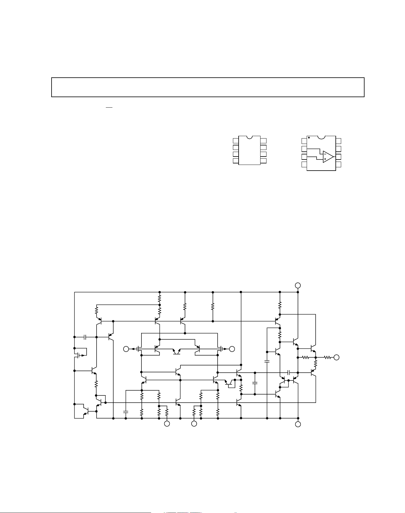
7
RB4
RB5
QB6
Z2
Q5
QB8
R2S
5
JB1
Z1
CB1
QB4
QB1
RB2
QB2
RB1
QB3
CC1
R1L
R1A
RB3
QB5
J1
Q1
Q3
R1P1
R1P2
R1S
1
Simplified Schematic
REV. 0
Information furnished by Analog Devices is believed to be accurate and
reliable. However, no responsibility is assumed by Analog Devices for its
use, nor for any infringements of patents or other rights of third parties
which may result from its use. No license is granted by implication or
otherwise under any patent or patent rights of Analog Devices.
Q8
Q9
RB6
QB7
R4
Q7
CC2
Q10
4
Q11
RS1
QS1
QS2
R5
RS2
RB7
Q2
J2
32
CCB
Q6
Q4 QS3
CF
R3
R2L
R2P1
R2P2
R2A
One Technology Way, P.O. Box 9106, Norwood. MA 02062-9106, U.S.A.
Tel: 617/329-4700 Fax: 617/326-8703
QB9
6
Page 2
OP176–SPECIFICATIONS
ELECTRICAL CHARACTERISTICS
(@ VS = ±15.0 V, TA = +25°C unless otherwise noted)
Parameter Symbol Conditions Min Typ Max Units
INPUT CHARACTERISTICS
Offset Voltage V
Offset Voltage V
Input Bias Current I
Input Offset Current I
Input Voltage Range V
OS
OS
B
OS
CM
Common-Mode Rejection CMRR V
Large Signal Voltage Gain A
Offset Voltage Drift ∆V
VO
/∆T5µV/°C
OS
–40°C ≤ TA ≤ +85°C 1.25 mV
VCM = 0 V 350 nA
= 0 V, –40°C ≤ TA ≤ +85°C 400 nA
V
CM
V
= 0 V ±50 nA
CM
= 0 V, –40°C ≤ TA ≤ +85°C ±100 nA
V
CM
–10.5 +10.5 V
= ±10.5 V,
CM
–40°C ≤ T
R
= 2 kΩ 250 V/mV
L
= 2 kΩ, –40°C ≤ TA ≤ +85°C 175 V/mV
R
L
= 600 Ω 200 V/mV
R
L
≤ +85°C 80 106 dB
A
1mV
OUTPUT CHARACTERISTICS
R
Output Voltage Swing V
Output Short Circuit Current I
O
SC
= 2 kΩ, –40°C ≤ TA ≤ +85°C –13.5 +13.5 V
L
= 600 Ω, VS = ±18 V –14.8 +14.8 V
R
L
±25 ±50 mA
POWER SUPPLY
Power Supply Rejection Ratio PSRR V
Supply Current I
Supply Current I
Supply Voltage Range V
SY
SY
S
= ±4.5 V to ±18 V 86 108 dB
S
–40°C ≤ T
V
= ±4.5 V to ±18 V, V
S
= ∞, –40°C ≤ TA ≤ +85°C 2.5 mA
R
L
V
= ±22 V, V
S
–40°C ≤ T
≤ +85°C80 dB
A
= 0 V, R
O
≤ +85°C 2.75 mA
A
= 0 V,
O
= ∞,
L
±4.5 ±22 V
DYNAMIC PERFORMANCE
Slew Rate SR R
= 2 kΩ 15 25 V/µs
L
Gain Bandwidth Product GBP 10 MHz
AUDIO PERFORMANCE
THD + Noise V
Voltage Noise Density e
Current Noise Density i
Specifications subject to change without notice.
n
n
= 3 V rms,
IN
= 2 kΩ, f = 1 kHz 0.001 %
R
L
f = 1 kHz 6 nV/√Hz
f = 1 kHz 0.5 pA/√Hz
–2–
REV. 0
Page 3
OP176
WAFER TEST LIMITS
(@ VS = ±15.0 V, TA = +25°C unless otherwise noted)
Parameter Symbol Conditions Limit Units
Offset Voltage V
Input Bias Current I
Input Offset Current I
Input Voltage Range
1
OS
B
OS
V
CM
Common-Mode Rejection CMRR V
VCM = 0 V 350 nA max
V
= 0 V ±50 nA max
CM
= ±10.5 V 80 dB min
CM
1 mV max
±10.5 V min
Power Supply Rejection Ratio PSRR V = ± 4.5 V to ±18 V 86 dB min
R
Large Signal Voltage Gain A
Output Voltage Range V
Supply Current I
NOTES
Electrical tests and wafer probe to the limits shown. Due to variations in assembly methods and normal yield loss, yield after packaging is not guaranteed for standard
product dice. Consult factory to negotiate specifications based on dice lot qualifications through sample lot assembly and testing.
1
Guaranteed by CMR test.
ABSOLUTE MAXIMUM RATINGS
Supply Voltage . . . . . . . . . . . . . . . . . . . . . . . . . . . . . . . . ±22 V
Input Voltage
Differential Input Voltage
2
. . . . . . . . . . . . . . . . . . . . . . . . . . . . . . . . . ±18 V
2
. . . . . . . . . . . . . . . . . . . . . . . ±7.5 V
VO
O
SY
1
= 2 kΩ 250 V/mV min
L
R
= 2 kΩ 13.5 V min
L
= ±18.0 V, RL = 600 Ω 14.8 V min
V
S
V
= ±22.0 V, V
S
= ±4.5 V to ±18 V, 2.5 mA max
V
S
VO = 0 V, R
= ∞
L
= 0 V, R
O
= ∞ 2.75 mA max
L
DICE CHARACTERISTICS
+
V
OUT
NULL
Output Short-Circuit Duration to GND . . . . . . . . . . Indefinite
Storage Temperature Range
P, S Package . . . . . . . . . . . . . . . . . . . . . . . .–65°C to +150°C
Operating Temperature Range
OP176G . . . . . . . . . . . . . . . . . . . . . . . . . . . .–40°C to +85°C
Junction Temperature Range
P, S Package . . . . . . . . . . . . . . . . . . . . . . . .–65°C to +150°C
Lead Temperature Range (Soldering, 60 sec) . . . . . . . +300°C
Package Type θ
3
JA
θ
JC
Units
NULL
–IN
+IN
–
V
8-Pin Plastic DIP (P) 103 43 °C/W
8-Pin SOIC (S) 158 43 °C/W
NOTES
1
Absolute maximum ratings apply to both DICE and packaged parts, unless
otherwise noted.
2
For input voltages greater than ±7.5 V limit input current to less than 5 mA.
3
θJA is specified for the worst case conditions, i.e., θ
for P-DIP packages; θ
package.
is specified for device soldered in circuit board for SOIC
JA
is specified for device in socket
JA
OP176 Die Size 0.069 × 0.067 Inch, 4,623 Sq. Mils.
Substrate (Die Backside) Is Connected to V–.
Transistor Count, 26.
ORDERING GUIDE
Model Temperature Range Package Description Package Option
OP176GP –40°C to +85°C 8-Pin Plastic DIP N-8
OP176GS –40°C to +85°C 8-Pin SOIC SO-8
OP176GSR –40°C to +85°C SO-8 Reel, 2500 Pieces
OP176GBC +25°C DICE
CAUTION
ESD (electrostatic discharge) sensitive device. Electrostatic charges as high as 4000 V readily
accumulate on the human body and test equipment and can discharge without detection.
Although the OP176 features proprietary ESD protection circuitry, permanent damage may
occur on devices subjected to high energy electrostatic discharges. Therefore, proper ESD
precautions are recommended to avoid performance degradation or loss of functionality.
REV. 0
–3–
WARNING!
ESD SENSITIVE DEVICE
Page 4
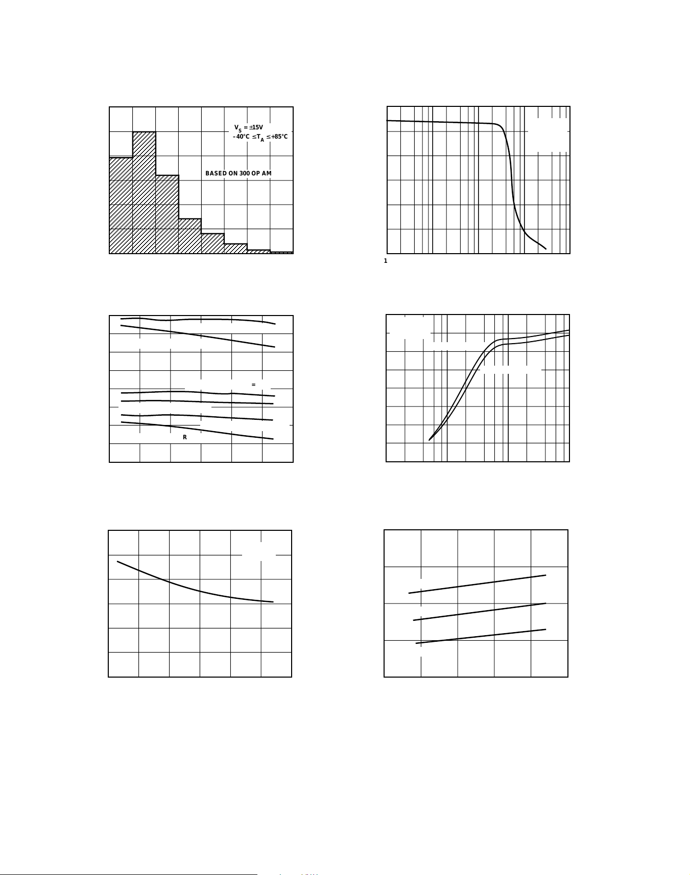
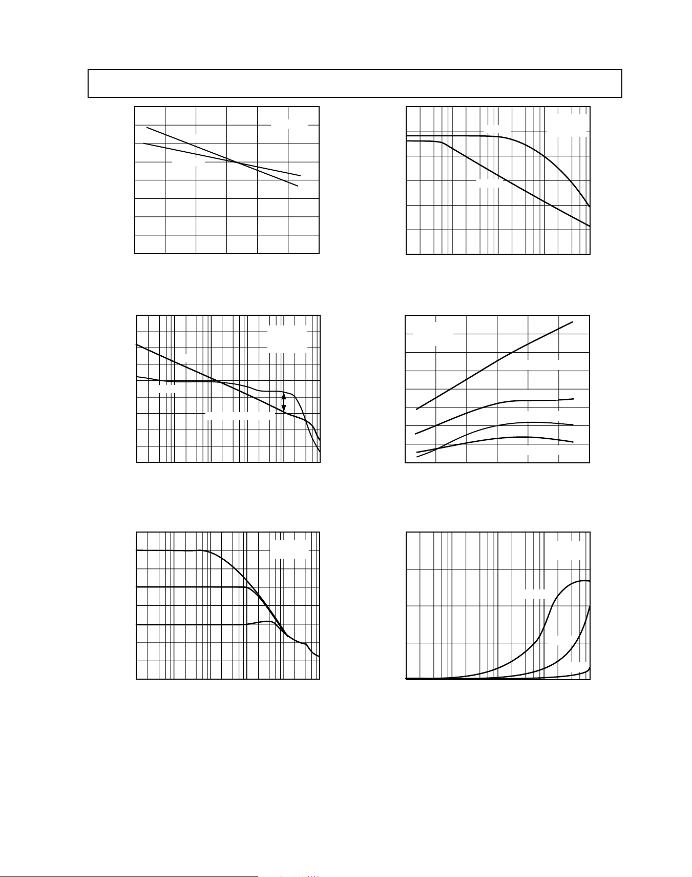
OP176–Typical Characteristics
120
100
80
60
40
20
±VS = ±15V
≤–40°C ≤ T
BASED ON 300 OP AMPS
0
1
0
µ
t
VOS – µV/°C
C
≤ +85°C
A
754362
8
30
25
20
15
10
MAXIMUM OUTPUT SWING – Volts
5
0
10k 10M1M100k1k
FREQUENCY – Hz
±VS = ±15V
ΩTA = +25°C
RL = 2kΩ
Figure 1. Input Offset Voltage Drift Distribution @ ±15 V Figure 4. Maximum Output Swing vs. Frequency
16
ΩVS = ±18V, +VOM, RL = 600Ω
ΩVS = ±18V, –VOM, RL = 600Ω
15
14
ΩVS = ±15V, –VOM, RL = 2kΩ
13
ΩVS = ±15V, –VOM, RL = 600Ω
ABSOLUTE OUTPUT VOLTAGE – V
ΩVS = ±15V, +VOM, RL = 2kΩ
ΩVS = ±15V, +VOM, RL = 600Ω
16
VS = ±15V
T
= +25°C
A
14
12
10
8
6
OUTPUT SWING – Volts
4
2
POSITIVE SWING
NEGATIVE SWING
12
–25–50
TEMPERATURE – °C
100
7550250
0
10 100 10k1k
ΩLOAD RESISTANCE – Ω
Figure 2. Output Swing vs. Temperature Figure 5. Maximum Output Swing vs. Load Resistance
300
250
200
150
100
INPUT BIAS CURRENT – nA
50
0
–50
–25
TEMPERATURE – °C
±VS = ±15V
V
= 0V
CM
7550250
100
2.50
2.25
TA = +85°C
2.00
SUPPLY CURRENT – mA
1.75
1.50
0
TA = +25°C
TA = –40°C
±5±
SUPPLY VOLTAGE – V
±15± ±20±±10±
±25±
Figure 3. Input Bias Current vs. Temperature Figure 6. Supply Current per Amplifier vs. Supply Voltage
–4–
REV. 0
Page 5
OP176
40
20
0
1k 1M100k10k100
10
30
FREQUENCY – Hz
ΩIMPEDANCE – Ω
AV = +100
AV = +10
AV = +1
TA = +25°C
V
S
= ±15V
80
70
60
50
40
30
20
ABSOLUTE OUTPUT CURRENT – mA
10
0
SINK
SOURCE
–25–50
TEMPERATURE – °C
±VS = ±15V
7550250
Figure 7. Short Circuit Current vs. Temperature @
120
100
80
60
40
20
GAIN – dB
–20
–40
–60
PHASE
0
1k 10k 100M10M1M100k
GAIN
PHASE MARGIN = 60°
FREQUENCY – Hz
TA = +25°C
VS = ±15V
R
= >600
L
Ω
100
±
15 V
90
135
180
225
POWER SUPPLY REJECTION – dB
Figure 10. Power Supply Rejection vs. Frequency
2000
1750
1500
1250
1000
PHASE – Degrees
OPEN-LOOP GAIN – V/mV
120
100
750
500
250
80
60
40
20
0
0
±VS = ±15V
±VO = ±10V
–25–50
–PSRR
1k 1M100k10k100
FREQUENCY – Hz
TEMPERATURE – °C
+PSRR
Ω–GAIN, RL = 2kΩ
+GAIN, RL = 2kΩ
–GAIN, RL = 600Ω
+GAIN, RL = 600Ω
TA = +25°C
±VS = ±15V
7550250
100
Figure 8. Open-Loop Gain & Phase vs. Frequency
50
40
30
20
10
GAIN – dB
0
–10
–20
–30
1k 10k 100M10M1M100k
FREQUENCY – Hz
TA = +25°C
V
= ±15V
S
Figure 11. Open-Loop Gain vs. Temperature
Figure 12. Closed-Loop Output Impedance vs. FrequencyFigure 9. Closed-Loop Gain vs. Frequency
REV. 0
–5–
Page 6
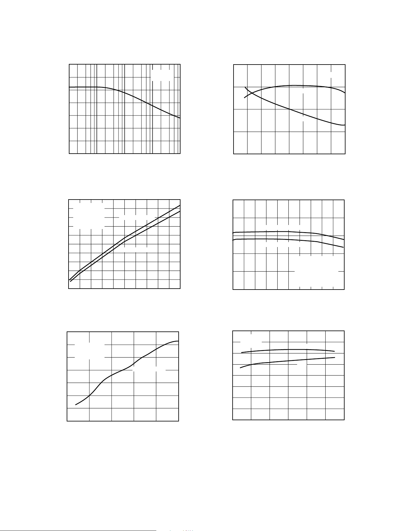
OP176
65
45
–75 125
60
50
–50
55
75 10050250–25
±VS = ±15V
14
6
12
8
10
TEMPERATURE – °C
PHASE MARGIN – Degrees
GAIN BANDWIDTH PRODUCT – MHz
PHASE
GAIN
40
0
100
10
5
–25–50
20
15
25
30
35
7550250
±VS = ±15V
ΩRL = 2kΩ
SLEW RATE – V/µs
TEMPERATURE – °C
SR–
SR+
140
120
100
80
60
40
COMMON-MODE REJECTION – dB
20
TA = +25°C
V
= ±15V
S
0
1k 1M100k10k100
FRERQUENCY – Hz
Figure 13. Common-Mode Rejection vs. Frequency
100
±VS = ±15V
90
ΩRL = 2kΩ
VIN = 100mVp-p
80
70
60
50
40
OVERSHOOT – %
30
20
10
0
= 1
AV
CL
100
0
LOAD CAPACITANCE – pF
NEGATIVE SWING
POSITIVE SWING
1000
900800700600500400300200
Figure 14. Small Signal Overshoot vs. Load Capacitance
35
Figure 16. Gain Bandwidth Product & Phase Margin vs.
Temperature
50
40
NEGATIVE SLEW RATE
30
POSITIVE SLEW RATE
20
SLEW RATE – V/µs
10
0
200
0
LOAD CAPACITANCE – pF
VS = ±15V
R
= 2kΩ
L
SWING = ±10V
SLEW WINDOW = ±5V
T
= +25°C
A
18001600140012001000800600400
2000
Figure 17. Slew Rate vs. Load Capacitance
30
ΩVS = ±15V
R
= 2kΩ
L
TA = +25°C
25
20
15
SLEW RATE – V/µs
10
5
0
0
Figure 15. Slew Rate vs. Differential Input Voltage
0.4
DIFFERENTIAL INPUT VOLTAGE – V
SR+ AND SR–
1.61.20.8
2.0
–6–
Figure 18. Slew Rate vs. Temperature
REV. 0
Page 7
25
10k
2.5
2.0
0
10 100 1k
1.5
1.0
0.5
FREQUENCY – Hz
CURRENT NOISE – pA/ Hz
VS = ±15V
T
A
= +25°C
±VS = ±15V
ΩTA = +25°C
20
15
10
VOLTAGE NOISE – nV/ Hz
5
0
10 100 10k1k
FREQUENCY – Hz
OP176
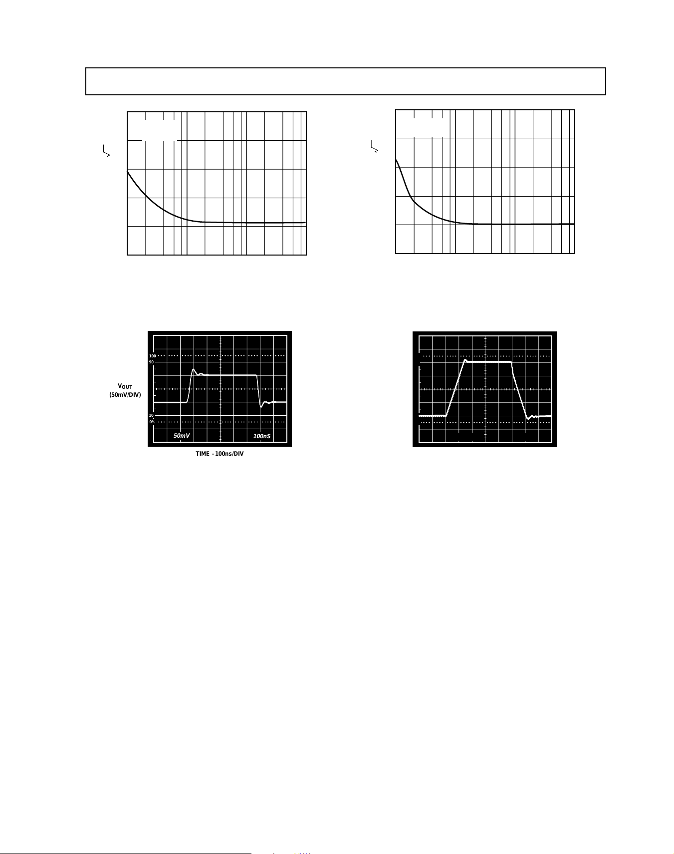
Figure 19. Voltage Noise Density vs. Frequency
100
90
V
OUT
(50mV/DIV)
10
0%
50mV
TIME –100ns/DIV
100nS
Figure 20. Small Signal Transient Response
Figure 21. Current Noise Density vs. Frequency
100
90
V
OUT
(5V/DIV)
10
0%
5V
TIME – 500ns/DIV
500nS
Figure 22. Large Signal Transient Response
REV. 0
–7–
Page 8

OP176
0.1
0.010
0.001
.0001
20 100 1k 10k 20k
±VS = ±18V
ΩRL = 600Ω
Ω10Vrms
Ω5Vrms
Ω3Vrms
Ω1Vrms
APPLICATIONS
Short Circuit Protection
The OP176 has been designed with output short circuit
protection. The typical output drive current is ± 50 mA. This
high output current and wide output swing combine to yield an
excellent audio amplifier, even when driving large signals, at low
power and in a small package.
Total Harmonic Distortion
Total Harmonic Distortion + Noise (THD + N) of the OP176
is well below 0.001% with any load down to 600 Ω. However,
this is dependent upon the peak output swing. In Figure 23 it is
seen that the THD + Noise with 3 V rms output is below
0.001%. In the following Figure 24, THD + Noise is below
0.001% for the 10 kΩ and 2 kΩ loads but increases to above
0.01% for the 600 Ω load condition. This is a result of the
output swing capability of the OP176. Notice the results in
Figure 25, showing THD vs. V
(V rms).
IN
0.1
±VS = ±15V
VO = 3Vrms
0.010
0.001
.0001
20 100 1k 10k 20k
Ω600Ω
FIGURE 23. THD + Noise vs. Frequency
0.1
±VS = ±18V
VO = 10Vrms
Figure 25. THD + Noise vs. Output Amplitude (V rms)
The output of the OP176 is designed to maintain low harmonic
distortion while driving 600 Ω loads. However, driving 600 Ω
loads with very high output swings results in higher distortion if
clipping occurs.
To attain low harmonic distortion with large output swings,
supply voltages may be increased. Figure 26 shows the performance of the OP176 driving 600 Ω loads with supply voltages
varying from ±18 volts to ±20 volts. Notice that with ± 18 volt
supplies the distortion is fairly high, while with ± 20 volt supplies
it is a very low 0.0007%.
0.1
ΩRL = 600Ω
0.010
VO = ±18V
0.010
0.001
0.0001
20 100 1k 10k 20k
Figure 24. THD + Noise vs. R
Ω600Ω
2kΩ
10kΩ
LOAD
0.001
VO = ±19V
0.0001
20 100 1k 10k 20k
VO = ±20V
Figure 26. THD + Noise vs. Supply Voltage
–8–
VO = ±22V
REV. 0
Page 9

OP176
OP176
1.4kΩ
1.4kΩ
–
+
2
3
6
Noise
The voltage noise density of the OP176 is below 6 nV/√Hz from
30 Hz. This enables low noise designs to have good performance throughout the full audio range. Figure 27 shows a
typical OP176 with a 1/f corner at 6 Hz.
10.0 µV /DIVCH A: 80.0 µV FS
Hz
50Hz /
BW:
300 mHz
\ 0 Hz
MKR:
MKR: 15.9 µV/
5.4 Hz
Figure 27. 1/f Noise Corner
Noise Testing
For audio applications the noise density is usually the most
important noise parameter. For characterization the OP176 is
tested using an Audio Precision, System One. The input signal
to the Audio Precision must be amplified enough to measure
accurately. For the OP176 the noise is gained by approximately
1020 using the circuit shown in Figure 28. Any readings on the
Audio Precision must then be divided by the gain. In implementing this test fixture, good supply bypassing is essential.
100Ω
OP176
909Ω
100Ω
OP37
909Ω
490Ω
OP37
4.42kΩ
OUTPUT
Figure 28. Noise Test
Upgrading “5534‘’ Sockets
The OP176 is a superior amplifier for upgrading existing
designs using the industry standard 5534. In most application
circuits, the OP176 can directly replace the 5534 without any
modifications to the surrounding circuitry. Like the 5534, the
OP176 follows the industry standard, single op amp pinout. The
difference between these two devices is the location of the null
pins and the 5534’s compensation capacitor.
The 5534 normally requires a 22 pF capacitor between Pins 5
and 8 for stable operation. Since the OP176 is internally
compensated for unity gain operation, it does not require
external compensation. Nevertheless, if the 5534 socket already
includes a capacitor, the OP176 can be inserted without
removing it. Since the OP176’s Pin 8 is a “NO CONNECT’’
pin, there is no internal connection to that pin. Thus, the 22 pF
capacitor would be electrically connected through Pin 5 to the
internal nulling circuitry. With the other end left open, the
capacitor should have no effect on the circuit. However, to
avoid altogether any possibility for noise injection, it is recommended that the 22 pF capacitor be cut out of the circuit
entirely.
If the original 5534 socket includes offset nulling circuitry, one
would find a 10 kΩ to 100 kΩ potentiometer connected between
Pins 1 and 8 with said potentiometer’s wiper arm connected to
V+. In order to upgrade the socket to the OP176, this circuit
should be removed before inserting the OP176 for its offset
nulling scheme uses Pins 1 and 5. Whereas the wiper arm of the
5534 trimming potentiometer is connected to the positive
supply, the OP176’s wiper arm is connected to the negative
supply. Directly substituting the OP176 into the original socket
would inject a large current imbalance into its input stage. In
this case, the potentiometer should be removed altogether, or, if
nulling is still required, the trimming potentiometer should be
rewired to match the nulling circuit as illustrated in Figure 29.
+V
S
7
2
V
OUT
3
OP176
1
4
–V
P1
S
6
5
ΩP1 = 10kΩ
V
TRIM RANGE = ±2mV
OS
Figure 29. Offset Voltage Nulling Scheme
Input Overcurrent Protection
The maximum input differential voltage that can be applied to
the OP176 is determined by a pair of internal Zener diodes
connected across its inputs. They limit the maximum differential input voltage to ±7.5 V. This is to prevent emitter-base
junction breakdown from occurring in the input stage of the
OP176 when very large differential voltages are applied.
However, in order to preserve the OP176’s low input noise
voltage, internal resistances in series with the inputs were not
used to limit the current in the clamp diodes. In small signal
applications, this is not an issue; however, in applications where
large differential voltages can be inadvertently applied to the
device, large transient currents can flow through these diodes.
Although these diodes have been designed to carry a current of
±5 mA, external resistors as shown in Figure 30 should be used
in the event that the OP176’s differential voltage were to exceed
±7.5 V.
Figure 30. Input Overcurrent Protection
REV. 0
–9–
Page 10

OP176
+15V
+
10µF
0.1µF
2
3
7
6
4
V
IN
V
OUT
R
L
2kΩ
–15V
10µF
0.1µF
OP176
Output Voltage Phase Reversal
Since the OP176’s input stage combines bipolar transistors for
low noise and p-channel JFETs for high speed performance, the
output voltage of the OP176 may exhibit phase reversal if either
of its inputs exceeds the specified negative common-mode input
voltage. This might occur in some applications where a transducer, or a system, fault might apply very large voltages upon
the inputs of the OP176. Even though the input voltage range
of the OP176 is ±10.5 V, an input voltage of approximately
–13.5 V will cause output voltage phase reversal. In inverting
amplifier configurations, the OP176’s internal 7.5 V clamping
diodes will prevent phase reversal; however, they will not
prevent this effect from occurring in noninverting applications.
For these applications, the fix is a 3.92 kΩ resistor in series
with the noninverting input of the device and is illustrated in
Figure 31.
RFB*
V
ΩR
L
2kΩ
OUT
V
IN
*R
FB
2
3
ΩR
S
3.92kΩ
IS OPTIONAL
OP176
6
Figure 31. Output Voltage Phase Reversal Fix
Overdrive Recovery
The overdrive recovery time of an operational amplifier is the
time required for the output voltage to recover to a rated output
level from a saturated condition. This recovery time is important in applications where the amplifier must recover quickly
after a large abnormal transient event. The circuit shown in
Figure 32 was used to evaluate the OP176’s overload recovery
time. The OP176 takes approximately 1 µs to recover to V
+10 V and approximately 900 ns to recover to V
2
3
R2
Ω10kΩ
OP176
6
V
IN
4Vp-p
@100Hz
R1
Ω1kΩ
R
S
909Ω
= –10 V.
OUT
V
OUT
R
L
Ω2.43kΩ
Figure 32. Overload Recovery Time Test Circuit
High Speed Operation
As with most high speed amplifiers, care should be taken with
supply decoupling, lead dress, and component placement.
Recommended circuit configurations for inverting and
noninverting applications are shown in Figure 33 and Figure 34.
OUT
Figure 33. Unity Gain Follower
+15V
10µF
+
0.1µF
10pF
4.99kΩ
V
IN
2.49kΩ
=
2
OP176
3
–15V
4.99kΩ
7
4
0.1µF
10µF
V
6
+
OUT
2kΩ
Figure 34. Unity Gain Inverter
In inverting and noninverting applications, the feedback
resistance forms a pole with the source resistance and capacitance (R
shown in Figure 35. With R
and CS) and the OP176’s input capacitance (CIN), as
S
and R
S
in the kΩ range, this pole
F
can create excess phase shift and even oscillation. A small
capacitor, C
setting R
, in parallel with RFB eliminates this problem. By
FB
+ CIN) = R
S (CS
, the effect of the feedback pole is
FB CFB
completely removed.
C
FB
R
FB
R
S
C
S
C
IN
V
OUT
–10–
Figure 35. Compensating the Feedback Pole
REV. 0
Page 11

OP176
6
2
3
A2
6
3
2
A1
3
2
6
A3
V
IN
V
O1
V
O2
R3
2kΩ
R9
50Ω
R11
1kΩ
P1
10kΩ
R12
1kΩ
R10
50Ω
R8
2kΩ
R2
2kΩ
R5
2kΩ
R4
2kΩ
R1
2kΩ
R7
2kΩ
R6
2kΩ
V
O2
– VO1 = V
IN
A1, A2, A3 = OP176
GAIN =
SET R2, R4, R5 = R1 AND R6, R7, R8 = R3
R3
R1
Attention to Source Impedances Minimizes Distortion
Since the OP176 is a very low distortion amplifier, careful
attention should be given to source impedances seen by both
inputs. As with many FET-type amplifiers, the p-channel
JFETs in the OP176’s input stage exhibit a gate-to-source
capacitance that varies with the applied input voltage. In an
inverting configuration, the inverting input is held at a virtual
ground and, as such, does not vary with input voltage. Thus,
since the gate-to-source voltage is constant, there is no distortion due to input capacitance modulation. In noninverting
applications, however, the gate-to-source voltage is not
constant. The resulting capacitance modulation can cause
distortion above 1 kHz if the input impedance is > 2 kΩ and
unbalanced.
Figure 36 shows some guidelines for maximizing the distortion
performance of the OP176 in noninverting applications. The
best way to prevent unwanted distortion is to ensure that the
parallel combination of the feedback and gain setting resistors
(R
and R
F
) is less than 2 kΩ. Keeping the values of these
G
resistors small has the added benefits of reducing the thermal
noise of the circuit and dc offset errors. If the parallel combination of R
F
resistor, R
V
and R
IN
is larger than 2 kΩ, then an additional
G
, should be used in series with the noninverting
S
R
G
RS*
R
F
OP176
* RS = RG//RF IF RG//RF > 2kΩ
FOR MINIMUM DISTORTION
V
OUT
Figure 36. Balanced Input Impedance to Mininize
Distortion in Noninverting Amplifier Circuits
R
V
IN
R
= R
X
R
=I+
C
F
R
G
[ ]
F
C
F
R
R
X
+
R
F
G
CLR
)
R
F
O
OP176
WHERE RO = OPEN-LOOP OUTPUT RESISTANCE
O RG
F
I
(
)(
|
A
|
CL
V
C
OUT
L
Figure 37. In-the-Loop Compensation Technique for
Driving Capacitive Loads
APPLICATIONS USING THE OP176
A High Speed, Low Noise Differential Line Driver
The circuit of Figure 38 is a unique line driver widely used in
many applications. With ±18 V supplies, this line driver can
deliver a differential signal of 30 V p-p into a 2.5 kΩ load. The
high slew rate and wide bandwidth of the OP176 combine to
yield a full power bandwidth of 130 kHz while the low noise
front end produces a referred-to-input noise voltage spectral
density of 15 nV/√
Hz. The circuit is capable of driving lower
impedance loads as well. For example, with a reduced output
level of 5 V rms (14 V p-p), the circuit exhibits a full-power
bandwidth of 190 kHz while driving a differential load of 249 Ω!
The design is a transformerless, balanced transmission system
where output common-mode rejection of noise is of paramount
importance. Like the transformer-based design, either output
can be shorted to ground for unbalanced line driver applications
without changing the circuit gain of 1. Other circuit gains can
be set according to the equation in the diagram. This allows the
design to be easily set for noninverting, inverting, or differential
operation.
input. The value of R
tion of R
and RG to maintain the low distortion performance of
F
is determined by the parallel combina-
S
the OP176. For a more generalized treatment on circuit
impedances and their effects on circuit distortion, please review
the section on Active Filters at the end of the Applications
section.
Driving Capacitive Loads
As with any high speed amplifier, care must be taken when
driving capacitive loads. The graph in Figure 14 shows the
OP176’s overshoot versus capacitive load. The test circuit is a
standard noninverting voltage follower; it is this configuration
that places the most demand on an amplifier’s stability. For
capacitive loads greater than 400 pF, overshoot exceeds 40%
and is roughly equivalent to a 45° phase margin. If the application requires the OP176 to drive loads larger than 400 pF, then
external compensation should be used.
Figure 37 shows a simple circuit which uses an in-the-loop
compensation technique that allows the OP176 to drive any
capacitive load. The equations in the figure allow optimization
of the output resistor, R
optimal circuit stability. One important note is that the circuit
bandwidth is reduced by the feedback capacitor, C
given by:
REV. 0
, and the feedback capacitor, CF, for
X
1
BW =
2 π R
F CF
, and is
F
Figure 38. A High Speed, Low Noise Differential Line
Driver
–11–
Page 12

OP176
1.0
0.1
0.010
0.001
20 100 1k 10k 20k
G = 2000
G = 200
G = 20
G = 4
±VS = ±18V
80kHz LPF
A Low Noise Microphone Preamplifier with a Phantom
Power Option
Figure 39 is an example of a circuit that combines the strengths
of the SSM2017 and the OP176 into a variable gain microphone preamplifier with an optional phantom power feature.
The SSM2017’s strengths lie in its low noise and distortion, and
gain flexibility/simplicity. However, rated only for 2 kΩ or
higher loads, this makes driving 600 Ω loads somewhat limited
with the SSM2017 alone. A pair of OP176s are used in the
circuit as a high current output buffer (U2) and a DC servo
stage (U3). The OP176’s high output current drive capability
provides a high level drive into 600 Ω loads when operating
from ±18 V supplies. For a complete treatment of the circuit
design details, the interested reader should consult application
note AN-242, available from Analog Devices.
This amplifier’s performance is quite good over programmed
gain ranges of 2 to 2000. For a typical audio load of 600 Ω,
THD + N at various gains and an output level of 10 V rms is
illustrated in Figure 40. For all but the very highest gain, the
THD + N is consistent and well below 0.01%, while the gain of
2000 becomes more limited by noise. The noise performance of
the circuit is exceptional with a referred-to-input noise voltage
spectral density of 1 nV/√
Hz at a circuit gain of 1000.
Figure 40. Low Noise Microphone Preamplifier THD + N
Performance at Various Gains (V
= 10 V rms and
OUT
RL = 600 Ω)
+
C8
47µF/
63V
R9
6.81kΩ
–IN
TO MICROPHONE
COMMON
+IN
NOTES:
1) Z1–Z4 1N752 (SEE TEXT).
2) C
3) GAIN = G = 2 x ((10k/RG ) +1) (SEE TEXT).
4) ALL RESISTORS 1% METAL FILM.
5) DOTTED PHANTOM POWER RELATED COMPONENTS OPTIONAL (SEE TEXT).
+48V
ΩR10
100Ω
R8
6.81kΩ
+
ΩR
C
1
P
IN
49.9Ω
47µF/
63V
+
ΩRP2
C
2
IN
49.9Ω
47µF/
63V
, CGX LOW LEAKAGE ELECTROLYTIC TYPES (SEE TEXT).
INX
PHANTOM POWER SUPPLY CONNECTIONS,
INTERLOCKED WITH +/–V
Z1
Z2
1)
RB1
10kΩ
4.7nF/
FILM
R
2
B
10kΩ
Z3
C
N
2200µF/ 10V
+
C
1
G
3)
R
G
C
2
G
+
2200µF/ 10V
Z4
1
(SEE NOTE 5).
S
+V
S
CRF2
100pF
7
3
8
1
5
2
4
C
1
RF
100pF
–V
S
U1
SSM2017P
6
R1
10kΩ
R7
1kΩ
10kΩ
+V
S
–V
R2
4
7
C1
7
4
–V
OP176
+V
S
S
U2
ΩR3
6
S
2
3
49.9Ω
R4
221kΩ
D1
1N458
D2
1N458
R5
221kΩ
C2
1µF FILM
C5
33pF
20kΩ
–V
S
2
3
+V
S
R6
1µF FILM
U3
OP176
6
C6
0.1µF
C7
0.1µF
+
C3
100µF/25V
+
C4
100µF/25V
OUT COMMON
+18V
–18V
OUTPUT
Figure 39. A Low Noise Microphone Preamplifier
–12–
REV. 0
Page 13

OP176
C1
100pF
R1
5.76kΩ
R2
5.62kΩ
ΩR5
51Ω
C2 100pF
R3
5.49kΩ
R4
5.62kΩ
ΩR6
51Ω
C4
0.01µF
U1
U2
C3
0.0047µF
C5
0.01µF
BALANCED
INPUTS
= AG, PIN 10 OR 18
V
IN
–
V
IN
+
TO
AD1878/
AD1879
SIGMADELTA
ADC
L & R
INPUTS
U1, U2 = OP176
–12V
ANALOG
(+)
(–)
NOTES
C1–C5 = NPO CERAMIC, NON-INDUCTIVE,
C3-C5 CLOSE TO ADC
R1–R6 = 1% METAL FILM
0.1µF
0.1µF
100µ/25V
+12V
ANALOG
COM
+V
S
–V
S
TO
U1, U2
100µ/25V
(+)
USE
FOR
SINGLE-ENDED
INPUTS
5kΩ
5kΩ
A Low Noise, +5 V/+10 V Reference
In many high resolution applications, voltage reference noise
can be a major contributor to overall system error. Monolithic
voltage references often exhibit too much wide band noise to be
used alone in these systems. Only through careful filtering and
buffering of these monolithic references can one realize wideband microvolt noise levels. The circuit illustrated in Figure 41
is an example of a low noise precision reference optimized for
both ac and dc performance around the OP176. With a +10 V
reference (the AD587), the circuit exhibits a 1 kHz spot output
noise spectral density < 10 nV/√
Hz. The reference output
voltage is selectable between 5 V and 10 V, depending only on
the selection of the monolithic reference. The output table
illustrated in the figure provides a selection of monolithic
references compatible with this circuit.
OUTPUT TABLE
4
TOLERANCE
(+/–mV)
5 TO 10
30 TO 100
30 TO 50
5 TO 30
2 TO 10
2.5 TO 20
15 TO 50
15 TO 25
6
5
R1
1kΩ
R2
10kΩ
R
TRIM
10kΩ
(OPTIONAL)
U2
OP176
R3
100Ω
C1
100µF/25V
C2
100µF/25V
R4
100Ω
4
2
C3
100µF/25V
R5
1.1kΩ
10µF/25V
6
7
3
V
OUT
R6
3.3Ω
C5
REF
COMMON
+15V
V
10V
10V
10V
10V
5V
5V
5V
5V
OUT
8
C4
0.1µF
U1
AD587
REF01
REF10
AD581
REF195
AD586
REF02
REF05
2
U1
A Differential ADC Driver
High performance audio sigma-delta ADCs, such as the stereo
16-bit AD1878 and the 18-bit AD1879, present challenging
design problems with regards to input interfacing. Because of
an internal switched capacitor input circuit, the ADC input
structure presents a difficult dynamic load to the drive amplifier
with fast transient input currents due to their 3 MHz ADC
sampling rate. Also, these ADCs inputs are differential with a
rated full-scale range of ±6.3 V, or about 4.4 V rms. Hence, the
ADC interface circuit of Figure 42 is designed to accept a
balanced input signal to drive the low dynamic impedances seen
at the inputs of these ADCs. The circuit uses two OP176
Figure 41. A Low Noise, +5 V/+10 V Reference
In operation, the basic reference voltage is set by U1, either a
5 V or 10 V 3-terminal reference chosen from the table. In this
case, the reference used is a 10 V buried Zener reference, but
all U1 IC types shown can plug into the pinout and can be
optionally trimmed. The stable 10 V from the reference is then
applied to the R1-C1-C2
noise filter, which uses electrolytic
capacitors for a low corner frequency. When electrolytic
capacitors are used for filtering, one must be cognizant of their
dc leakage current errors. Here, however, a dc bootstrap of C1
is used, so this capacitor sees only the small R2 dc drop as bias,
effectively lowering its leakage current to negligible levels. The
resulting low noise, dc-accurate output of the filter is then
buffered by a low noise, unity gain op amp using an OP176.
With the OP176’s low V
the dc performance of this circuit is quite good and will not
compromise voltage reference accuracy and/or drift. Also, the
OP176 has a typical current limit of 50 mA, so it can provide
higher output currents when compared to a typical IC reference
alone.
REV. 0
and control of the source resistances,
OS
Figure 42. A Balanced Driver Circuit for Sigma-Delta ADCs
amplifiers as inverting low-pass filters for their speed and high
output current drive. The outputs of the OP176s then drive the
differential ADC inputs through an RC network. This RC
network buffers the amplifiers against step changes at the ADC
sampling inputs using one differential (C3) and two commonmode connected capacitors (C4 and C5). The 51 Ω series
resistors isolate the OP176s from the heavily capacitive loads,
while the capacitors absorb the transient currents. Operating on
±12 V supplies, this circuit exhibits a very low THD + N of
0.001% at 5 V rms outputs. For single-ended drive sources, a
third op amp unity gain inverter can be added between R2’s (+)
input terminal and R4. For best results, short-lead, noninductive capacitors are suggested for C3, C4, and C5 (which are
placed close to the ADC), and 1% metal-film types for R1
through R6. For surface mount PCBs, these components can
be NPO ceramic chip capacitors and thin-film chip resistors.
–13–
Page 14

OP176
An RIAA Phono Preamp
Figure 43 illustrates a simple phono preamplifier using RIAA
equalization. The OP176 is used here to provide gain and is
chosen for its low input voltage noise and high speed performance. The feedback equalization network (R1, R2, C1, and
C2) forms a three time constant network, providing reasonably
accurate equalization with standard component values. The
input components terminate a moving magnet phono cartridge
as recommended by the manufacturer, the element values
shown being typical. When this ac coupled circuit is built with a
low noise bipolar input device such as the OP176, amplifier bias
current makes direct cartridge coupling difficult. This circuit
uses input and output capacitor coupling to minimize biasing
interactions.
Input ac coupling to the amplifier is provided via C5, and the
low frequency termination resistance, R
, is the parallel equiva-
T
lent of R6 and R7. R3 of the feedback network is ac grounded
via C4, a large value electrolytic. Additionally, this resistor is
set to a low value to minimize circuit noise from nonamplifier
sources. These design measures reduce the dc offset at the
output of the OP176 to a few millivolts. The output coupling
network of C3 and R4 is shown as suitable for wide band
response, but it can be set to a 7950 µs time constant for use as
a 20 Hz rumble filter.
The 1 kHz gain (“G”) of this circuit, controlled by R3, is
calculated as:
G (@ 1 kHz) = 0.101 × 1 +
R1
R3
For an R3 of 200 Ω, the circuit gain is just under 50 × (≈ 34 dB),
and higher gains are possible by decreasing R3. For any value
of R3, the R5-C6 time constant should be equal to R3 and the
series equivalent of C1 and C2.
Using readily available standard values for network elements
(R1, R2, C1, and C2) makes the design easily reproducible and
inexpensive. These components are ideally high quality
precision types, for low equalization errors and minimum
parasitics. One percent metal-film resistors and two percent
film capacitors of polystyrene or polypropylene are recommended. Using the suggested values, the frequency response
relative to the ideal RIAA characteristic is within ± 0.2 dB over
20 Hz–20 kHz. Even tighter response can be achieved by using
the alternate values, shown in brackets “[ ],” with the trade-off
of a non off-the-shelf part.
As previously mentioned, the OP176 was chosen for three
reasons: (1) For optimal circuit noise performance, the
amplifier used should exhibit voltage and current noise densities
of 5 nV/√
Hz and 1 pA/√Hz, respectively. (2) For high gain
accuracy, especially at high stage gains, the amplifier should
exhibit a gain bandwidth product in excess of 5 MHz. (3)
Equally important because of the 100% feedback through the
network at high frequencies, the amplifier must be unity gain
stable. With the OP176, the circuit exhibits low distortion over
the entire range, generally well below 0.01% at outputs levels of
rms using ±18 V supplies. To achieve maximum perfor-
5 V
mance from this high gain, low level circuit, power supplies
should be well regulated and noise free, and care should be
taken with shielding and conductor layout.
Active Filter Circuits Using the OP176
A general active filter topology that lends itself to both high-pass
(HP) and low-pass (LP) filters is the well known Sallen-Key
(SK) VCVS (Voltage-Controlled, Voltage Source) architecture.
This filter type uses the op amp as a fixed gain voltage follower
at either unity or a higher gain. Discussed here are simplified 2pole, unity gain forms of these filters, which are attractive for
several reasons: One, at audio frequencies, using an amplifier
with a 10 MHz bandwidth such as the OP176, these filters
exhibit reasonably low sensitivities for unity gain and high
damping (low Q). Second, as voltage followers, they are also
inherently gain accurate within their pass band; hence, no gain
resistor scaling errors are generated. Third, they can also be
made “dc accurate,” with output dc errors of only a few
millivolts. The specific filter response in terms of HP, LP and
damping is determined by the RC network around the op amp,
as shown in Figure 44a.
MOVING
MAGNET
PICKUP
Ω100kΩ
+V
S
1%
100µF
100µF
100µF/25V
C1
0.03µF
2%
R2
0.1µF
0.1µF
–V
S
7
6
4
100kΩ
[97.6kΩ
R1
1%
]
S
[7.87kΩ]
8.25kΩ
R3
C4
1000µF/16V
C5
100µF/25V
R6
–
C
t
150pF
Rt = R6| |R7
~ 50kΩ
ΩR7
100kΩ
+V
3
U1
OP176
2
–V
S
Ω200Ω (34dB)
Ω100Ω (40dB)
C3
C2
0.01µF
2%
100kΩ
ΩR4
+18V
–18V
ΩR5
499Ω
V
C6
3nF
OUT
Figure 43. An RIAA Phono Preamplifier Circuit
–14–
REV. 0
Page 15

OP176
100 50k 10k 1k 20
10.000
–30.00
–70.00
–50.00
–10.00
–20.00
–40.00
–60.00
0.0
LP
HP
FREQUENCY – Hz
dBr
High Pass Sections
Figure 44a illustrates the high-pass form of a 2-pole SK filter
using an OP176. For simplicity and practicality, capacitors C1
and C2
are set equal (“C”), and resistors R2 and R1 are
adjusted to a ratio, N, which provides the filter damping
coefficient, α, as per the design expressions. This high pass
design is begun with selection of standard capacitor values for
C1 and C2 and a calculation of N. The values for R1 and R2
are then determined from the following expressions:
R1
=
π×
2
1
FREQ×C×N
and
R2=N×R1
C1
0.01µF
C2
0.01µF
R2
22k
(22.508k)
OP176
3
2
Z
COMP
IN (–)
R1
11k
(11.254k)
+V
S
7
6
4
–V
S
Z
COMP
(HIGH PASS)
OUTPUT
R2
C2
C1
R1
OUT IN
GIVEN: α, FREQ
SET C1 = C2 = C
1
2
α = =
R1 =
R2 = N x R1
1 kHz BW SHOWN
Q
N
4
R2
N = =
2
R1
α
2 π FREQ x C x N
1
Low Pass Sections
In the LP SK arrangement of Figure 44b, the R and C elements
are interchanged where the resistors are made equal. Here, the
ratio of C2/C1 (“M”) is used to set the filter α, as noted.
Otherwise, this filter is similar to the HP section, and the
resulting 1 kHz LP response is shown in Figure 45. The design
begins with a choice of a standard capacitor value for C1 and a
calculation of M. This then forces a value of “M × C1” for C2.
Then, the value for R1 and R2 (“R”) is calculated according to
the following equation:
1
FREQ×C1×M
C1
0.02µF
S
6
S
R1
GIVEN: α, FREQ
α
= =
M = =
CHOOSE C1
C2 = M x C1
R =
1 kHz BW SHOWN
+V
7
4
–V
Z
COMP
(LOW PASS)
OUTPUT
C2
C1
OUT IN
1
2
Q
M
4
C2
2
C1
α
1
2 π FREQ x C1 x M
R1
11k
(11.254k)
R2
11k
(11.254k)
C2
0.01µF
R
=
2
π×
OP176
3
2
Z
COMP
IN (–)
R2
Figures 44a. Two-Pole Unity Gain HP/LP Active Filters
In this examples, circuit α (or 1/Q) is set equal to √2, providing
a Butterworth (maximally flat) characteristic. The filter corner
frequency is normalized to 1 kHz, with resistor values shown in
both rounded and (exact) form. Various other 2-pole response
shapes are possible with appropriate selection of α, and frequency can be easily scaled, using inversely proportional R or
C values for a given α. The 22 V/µs slew rate of the OP176 will
support 20 V p-p outputs above 100 kHz with low distortion.
The frequency response resulting with this filter is shown as the
dotted HP portion of Figure 45.
Figures 44b. Two-Pole Unity Gain HP/LP Active Filters
Figure 45. Relative Frequency Response of 2-Pole, 1 kHz
Butterworth LP (Left) and HP (Right) Active Filters
REV. 0
–15–
Page 16

OP176
Passive Component Selection for Active Filters
The passive components suitable for active filters deserve more
than casual attention. Resistors should be 1%, low TC, metalfilm types of the RN55 or RN60 style. Capacitors should be 1%
or 2% film types preferably, such as polypropylene or polystyrene, or NPO (COG) ceramic for smaller values.
Active Filter Circuit Subtleties
In designing active filter circuits with the OP176, moderately
low values (10 kΩ or less) for R1 and R2 can be used to
minimize the effects of Johnson noise when critical. The
practical tradeoff is, of course, capacitor size and expense. DC
errors will result for larger values of resistance, unless compensation for amplifier input bias current is used. To add bias
compensation in the HP filter section of Figure 42a, a feedback
compensation resistor equal to R2 can be used. This will
minimize bias current induced offset to the product of the
OP176’s I
and R2. For an R2 of 25 kΩ, this produces a typical
OS
compensated offset voltage of 50 µV. Similar compensation is
applied to Figure 42b, using a resistance equal to R1+ R2.
Using dc compensation, filter output dc errors using the OP176
will be dominated by its V
, which is typically 1 mV or less. A
OS
caveat here is that the additional resistors can increase noise
substantially. For example, a 10 kΩ resistor generates ~ 12 nV/
Hz of noise and is about twice that of the OP176. These
√
resistors can be ac bypassed to eliminate their noise using a
simple shunt capacitor chosen such that its reactance (X
C
) is
much less than R at the lowest frequency of interest.
A more subtle form of ac degradation is also possible in these
filters, namely nonlinear input capacitance modulation. This
issue was previously covered for general cases in the section on
minimizing distortion. In active filter circuits, a fully compensating network (for both dc and ac performance) can be used to
minimize this distortion. To be most effective, this network
) should include R1 through C2 as noted for either filter
(Z
COMP
type, of the same style and value as their counterparts in the
forward path. The effects of a Z
network on the THD + N
COMP
performance of two 1 kHz HP filters is illustrated in Figure 46.
One filter (A) is the example shown in Figure 44a (Curves A1
and A2), while the second (B) uses RC values scaled 10 times
upward in impedance (Curves B1 and B2). Both filters operate
with a 2 V rms input, ±18 V supplies, 100 kΩ loading, and
analyzer bandwidth of 80 kHz.
1
0.1
0.010
THD +N – %
0.001
0.0001
20 100 20k 1k
FREQUENCY – Hz
B1
A1
B2
A2
10 k
Figure 46. THD + N (%) vs. Frequency for Various 1 kHz HP
Active Filters Illustrating the Effects of the Z
Curves A1 and B1 show performance with Z
while curves A2 and B2 illustrate operation with Z
COMP
Network
COMP
shorted,
COMP
active.
For the “A” example values, distortion in the pass band of
1 kHz–20 kHz is below 0.001% compensated, and slightly
higher uncompensated. With the higher impedance “B” network, there is a much greater difference between compensated
and uncompensated responses, underscoring the sensitivity to
higher impedances. Although the positive effect of Z
COMP
is seen
for both “A” and “B” cases, there is a buffering effect which
takes place with lower impedances. As case “A” shows, when
using larger capacitance values in the source, the amplifier’s
nonlinear C-V input characteristics have less effect on the
signal.
Thus, to minimize the necessity for the complete Z
COMP
com-
pensation, effective filter designs should use the lowest capacitive impedances practical, with an 0.01 µF lower value limit as a
goal for lowest distortion (while lower values can certainly be
used, they may suffer higher distortion without the use of full
compensation). Since most designs are likely to use low relative
impedances for reasons of low noise and offset, the effects of
CM distortion may or may not actually be apparent to a given
application.
–16–
REV. 0
Page 17

OP176
97
E
I
1
P
–IN
+IN
98
CM2
2
C
IN
I
OS
1
Q1
D1
36
D2
CM1
98
R
5
7
EN E
5
R
3
4
R
6
8
9
Q2
OS
3
35
V
N1
D
N1
10
D
N2
V
N2
11
12
V
N3
D
N3
13
C
D
N4
V
N4
N1
14
15
V
N5
D
N5
16
D
N6
V
N6
C
1
17
6
C
2
R
4
E
M
97
V
2
19
D
3
G
1
R
7
G
C
2
3
98
21
R
9
R
G
22
8
C
4
23
3
R10C
G
5
24
4
R11C
E
6
C7
25
R
2
26
12
R
13
98
D
4
20
V
3
E
REF
51
99
G6
33
G7
D8
G8
V
4
F
1
V
5
F
2
G9
D10
R
17
L
2
29
34
R
18
D7
R
15
I
SY
28
D5
30
27
G5
C8
R
14
98
R
16
C
9
31
D6
32
D9
50
Figure 47. OP176 Spice Model Schematic
REV. 0
–17–
Page 18

OP176
OP176 SPICE Model
*
* Node Assignments
* Noninverting Input
* | Inverting Input
* | | Positive Supply
* | | | Negative Supply
* | | | | Output
*|||||
*|||||
.SUBCKT OP176 1 2 99 50 34
*
* INPUT STAGE & POLE AT 100 MHz
*
R3 5 51 2.487
R4 6 51 2.487
CIN 1 2 3.7E-12
CM1 1 98 7.5E-12
CM2 2 98 7.5E-12
C2 5 6 320E-12
I1 97 4 100E-3
IOS 1 2 1E-9
EOS 9 3 POLY(1) (26,28) 0.2E-3 1
Q1 5 2 7 QX
Q2 6 9 8 QX
R5 7 4 1.970
R6 8 4 1.970
D1 2 36 DZ
D2 1 36 DZ
EN 3 1 (10,0) 1
GN1 0 2 (13,0) 1E-3
GN2 0 1 (16,0) 1E-3
*
EREF98 0 (28,0) 1
EP 97 0 (99,0) 1
EM 51 0 (50,0) 1
*
* VOLTAGE NOISE SOURCE
*
DN1 35 10 DEN
DN2 10 11 DEN
VN1 35 0 DC 2
VN2 0 11 DC 2
*
* CURRENT NOISE SOURCE
*
DN3 12 13 DIN
DN4 13 14 DIN
VN3 12 0 DC 2
VN4 0 14 DC 2
*
* CURRENT NOISE SOURCE
*
DN5 15 16 DIN
DN6 16 17 DIN
VN5 15 0 DC 2
VN6 0 17 DC 2
*
* GAIN STAGE & DOMINANT POLE AT 32 Hz
*
R7 18 98 1.243E6
C3 18 98 4E-9
G1 98 18 (5,6) 4.021E-1
V2 97 19 1.35
V3 20 51 1.35
D3 18 19 DX
D4 20 18 DX
*
* POLE/ZERO PAIR AT 1.5 MHz/2.7 MHz
*
R8 21 98 1E3
R9 21 22 1.25E3
C4 22 98 47.2E-12
G2 98 21 (18,28) 1E-3
*
* POLE AT 100 MHz
*
R10 23 98 1
C5 23 98 1.59E-9
G3 98 23 (21,28) 1
*
* POLE AT 100 MHz
*
R11 24 98 1
C6 24 98 1.59E-9
G4 98 24 (23,28) 1
*
* COMMON-MODE GAIN NETWORK WITH ZERO AT
1 kHz
*
R12 25 26 1E6
C7 25 26 60E-12
R13 26 98 1
E2 25 98 POLY(2) (1,98) (2,98) 0 2.50 2.50
*
* POLE AT 100 MHz
*
R14 27 98 1
C8 27 98 1.59E-9
G5 98 27 (24,28) 1
*
* OUTPUT STAGE
*
R15 28 99 58.333E3
R16 28 50 58.333E3
C9 28 50 1E-6
ISY 99 50 1.743E-3
R17 29 99 100
R18 29 50 100
L2 29 34 1E-9
G6 32 50 (27,29) 10E-3
G7 33 50 (29,27) 10E-3
G8 29 99 (99,27) 10E-3
G9 50 29 (27,50) 10E-3
V4 30 29 1.74
V5 29 31 1.74
F1 29 0 V4 1
F2 0 29 V5 1
D5 27 30 DX
D6 31 27 DX
D7 99 32 DX
D8 99 33 DX
D9 50 32 DY
D10 50 33 DY
*
* MODELS USED
*
.MODEL QX PNP(BF=5E5)
.MODEL DX D(IS=1E-12)
.MODEL DY D(IS=1E-15 BV=50)
.MODEL DZ D(IS=1E-15 BV=7.0)
.MODEL DEN D(IS=1E-12 RS=4.35K KF=1.95E-15 AF=1)
.MODEL DIN D(IS=1E-12 RS=268 KF=1.08E-15 AF=1)
.ENDS OP176
–18–
REV. 0
Page 19

OUTLINE DIMENSIONS
Dimensions shown in inches and (mm).
8-Lead Plastic DIP (N-8)
OP176
PIN 1
0.210
(5.33)
MAX
0.160 (4.06)
0.115 (2.93)
0.022 (0.558)
0.014 (0.356)
0.0098 (0.25)
0.0040 (0.10)
8
1
0.430 (10.92)
0.348 (8.84)
0.100
(2.54)
BSC
5
4
0.070 (1.77)
0.045 (1.15)
0.280 (7.11)
0.240 (6.10)
0.060 (1.52)
0.015 (0.38)
0.130
(3.30)
MIN
SEATING
PLANE
8-Lead Narrow-Body SO (SO-8)
5
4
0.0192 (0.49)
0.0138 (0.35)
0.1574 (4.00)
0.1497 (3.80)
0.2440 (6.20)
0.2284 (5.80)
0.0688 (1.75)
0.0532 (1.35)
0.0098 (0.25)
0.0075 (0.19)
PIN 1
8
1
0.1968 (5.00)
0.1890 (4.80)
0.0500
(1.27)
BSC
0.325 (8.25)
0.300 (7.62)
0.015 (0.381)
0.008 (0.204)
0.0196 (0.50)
0.0099 (0.25)
8°
0°
0.195 (4.95)
0.115 (2.93)
x 45°
0.0500 (1.27)
0.0160 (0.41)
REV. 0
–19–
Page 20

C1878–10–1/94
–20–
PRINTED IN U.S.A.
Page 21

FOR CATALOG
ORDERING GUIDE
Model Temperature Range Package Description Package Option*
OP176GP –40°C to +85°C 8-Pin Plastic DIP N-8
OP176GS –40°C to +85°C 8-Pin SOIC SO-8
OP176GSR –40°C to +85°C SO-8 Reel, 2500 Pieces
OP176GBC +25°C DICE
*For outline information see Package Information section.
OP176
REV. 0
–21–
 Loading...