

Page 1
Ultralow Offset Voltage
V
V
G
www.BDTIC.com/ADI
FEATURES
Low VOS: 75 μV maximum
Low V
Ultrastable vs. time: 1.5 μV per month maximum
Low noise: 0.6 μV p-p maximum
Wide input voltage range: ±14 V typical
Wide supply voltage range: 3 V to 18 V
125°C temperature-tested dice
APPLICATIONS
Wireless base station control circuits
Optical network control circuits
Instrumentation
Sensors and controls
Precision filters
GENERAL DESCRIPTION
The OP07 has very low input offset voltage (75 μV maximum for
OP07E) that is obtained by trimming at the wafer stage. These
low offset voltages generally eliminate any need for external
nulling. The OP07 also features low input bias current (±4 nA for
the OP07E) and high open-loop gain (200 V/mV for the OP07E).
The low offset and high open-loop gain make the OP07
particularly useful for high gain instrumentation applications.
drift: 1.3 μV/°C maximum
OS
Thermocouples
Resistor thermal detectors (RTDs)
Strain bridges
Shunt current measurements
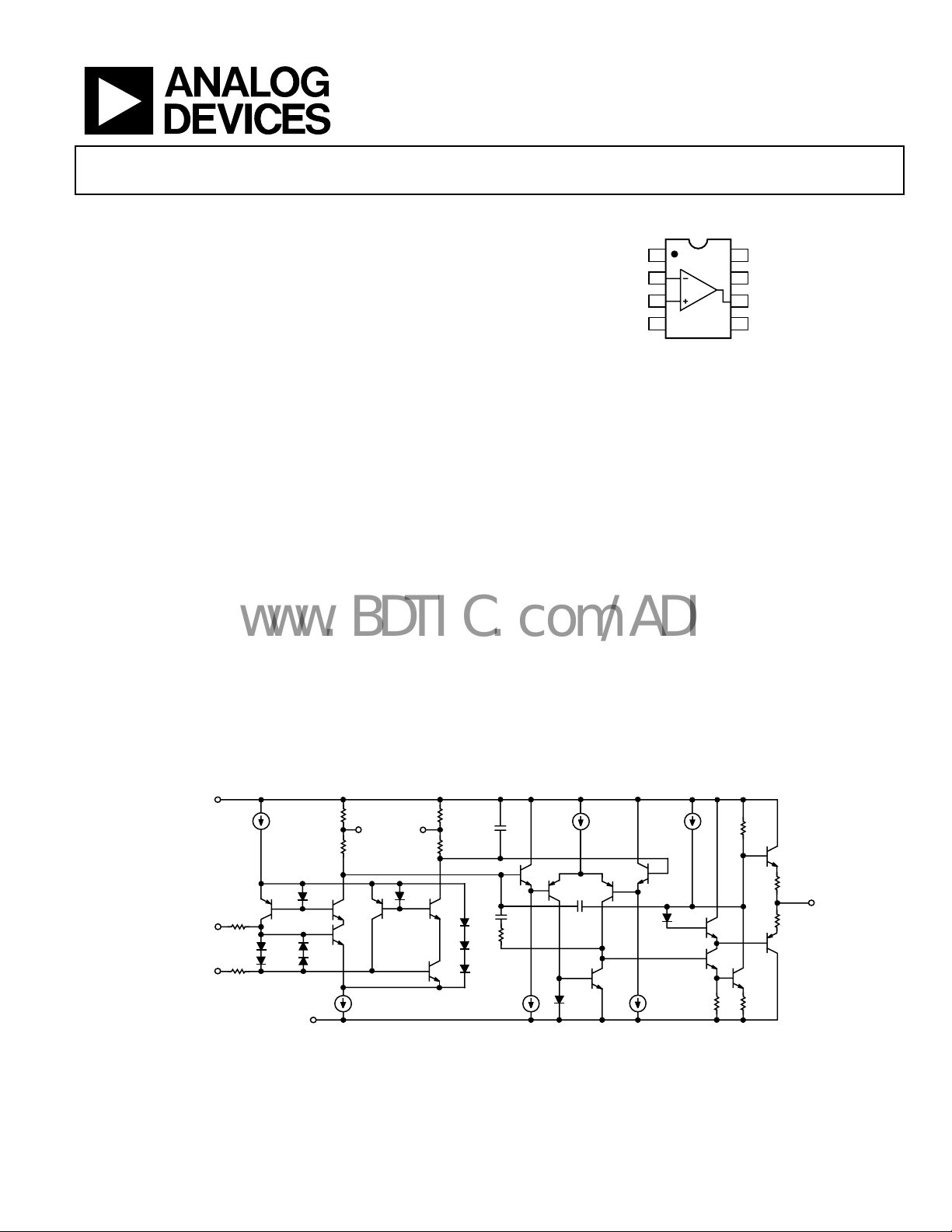
Operational Amplifier
OP07
PIN CONFIGURATION
OS
–IN
+IN
V–
OP07
2
3
4
NC = NO CONNECT
1
TRIM
Figure 1.
The wide input voltage range of ±13 V minimum combined
with a high CMRR of 106 dB (OP07E) and high input
impedance provide high accuracy in the noninverting circuit
configuration. Excellent linearity and gain accuracy can be
maintained even at high closed-loop gains. Stability of offsets
and gain with time or variations in temperature is excellent. The
accuracy and stability of the OP07, even at high gain, combined
with the freedom from external nulling have made the OP07 an
industry standard for instrumentation applications.
The OP07 is available in two standard performance grades. The
OP07E is sp
ecified for operation over the 0°C to 70°C range,
and the OP07C is specified over the −40°C to +85°C
temperature range.
The OP07 is available in epoxy 8-lead PDIP and 8-lead narrow
SOI
C packages. For CERDIP and TO-99 packages and standard
microcircuit drawing (SMD) versions, see the OP77.
8
VOS TRIM
7
V+
6
OUT
5
NC
0316-001
+
7
Q5
NONINVERTI N
INPUT
INVERTING
INPUT
1
R2A AND R2B ARE ELECTRONICALLY ADJUST ED ON CHIP AT FACTORY FOR MINIMUM INPUT OF FSET VO LTAGE.
Rev. D
Information furnished by Analog Devices is believed to be accurate and reliable. However, no
responsibility is assumed by Anal og Devices for its use, nor for any infringements of patents or ot her
rights of third parties that may result from its use. Specifications subject to change without notice. No
license is granted by implication or otherwise under any patent or patent rights of Analog Devices.
Trademarks and registered trademarks are the property of their respective owners.
R3
3
2
Q21
Q22
R4
1
R2A
R1A
Q7
Q23
Q24
4
V–
1
Q3 Q6
Q1
(OPTIONAL
NULL)
Q8
R2B
8
R1B
Q4
Q2
Figure 2. Simplified Schematic
1
Q16
Q15
R7
Q19
R9
OUT
6
R10
Q20
Q18
R8
R6
00316-002
C1
Q9
Q11
C3
Q27
R5
Q26
Q25
One Technology Way, P.O. Box 9106, Norwood, MA 02062-9106, U.S.A.
Tel: 781.329.4700 www.analog.com
Fax: 781.461.3113 ©2006 Analog Devices, Inc. All rights reserved.
C2
Q13
Q10
Q12
Q17
Q14
Page 2

OP07
www.BDTIC.com/ADI
TABLE OF CONTENTS
Features.............................................................................................. 1
Absolute Maximum Ratings ............................................................6
Applications....................................................................................... 1
General Description ......................................................................... 1
Pin Configuration............................................................................. 1
Revision History ............................................................................... 2
Specifications..................................................................................... 3
OP07E Electrical Characteristics ............................................... 3
OP07C Electrical Characteristics ............................................... 4
REVISION HISTORY
7/06—Rev. C. to Rev D
Changes to Features.......................................................................... 1
Changes to General Description .................................................... 1
Changes to Specifications Section.................................................. 3
Changes to Table 4............................................................................ 6
Changes to Figure 6 and Figure 8................................................... 7
Changes to Figure 13 and Figure 14............................................... 8
Changes to Figure 20........................................................................ 9
Changes to Figure 21 to Figure 25................................................ 10
Changes to Figure 26 and Figure 30............................................. 11
Replaced Figure 28 .........................................................................11
Changes to Applications Information Section............................ 12
Updated Outline Dimensions....................................................... 13
Changes to Ordering Guide.......................................................... 14
8/03—Rev. B to Rev. C
hanges to OP07E Electrical Specifications................................. 2
C
Changes to OP07C Electrical Specifications................................. 3
Edits to Ordering Guide .................................................................. 5
Edits to Figure 6................................................................................ 9
Updated Outline Dimensions....................................................... 11
Thermal Resistance.......................................................................6
ESD Caution...................................................................................6
Typical Performance Characteristics..............................................7
Typical Applications....................................................................... 11
Applications Information.......................................................... 12
Outline Dimensions....................................................................... 13
Ordering Guide .......................................................................... 14
3/03—Rev. A to Rev. B
pdated Package Titles......................................................Universal
U
Updated Outline Dimensions....................................................... 11
2/02—Rev. 0 to Rev. A
dits to Features.................................................................................1
E
Edits to Ordering Guide...................................................................1
Edits to Pin Connection Drawings .................................................1
Edits to Absolute Maximum Ratings..............................................2
Deleted Electrical Characteristics .............................................. 2–3
Deleted OP07D Column from Electrical Characteristics....... 4–5
Edits to TPCs ................................................................................ 7–9
Edits to High-Speed, Low V
Composite Amplifier ...................9
OS
Rev. D | Page 2 of 16
Page 3
OP07
www.BDTIC.com/ADI
SPECIFICATIONS
OP07E ELECTRICAL CHARACTERISTICS
VS = ±15 V, unless otherwise noted.
Table 1.
Parameter Symbol Conditions Min Typ Max Unit
INPUT CHARACTERISTICS
TA = 25°C
Input Offset Voltage
Long-Term VOS Stability
1
2
Input Offset Current IOS 0.5 3.8 nA
Input Bias Current IB ±1.2 ±4.0 nA
Input Noise Voltage en p-p 0.1 Hz to 10 Hz
Input Noise Voltage Density en fO = 10 Hz 10.3 18.0 nV/√Hz
f
f
Input Noise Current In p-p 14 30 pA p-p
Input Noise Current Density In fO = 10 Hz 0.32 0.80 pA/√Hz
f
f
Input Resistance, Differential Mode
4
Input Resistance, Common Mode R
Input Voltage Range IVR ±13 ±14 V
Common-Mode Rejection Ratio CMRR VCM = ±13 V 106 123 dB
Power Supply Rejection Ratio PSRR VS = ±3 V to ±18 V 5 20 μV/V
Large Signal Voltage Gain AVO RL ≥ 2 kΩ, VO = ±10 V 200 500 V/mV
R
0°C ≤ TA ≤ 70°C
Input Offset Voltage
Voltage Drift Without External Trim
Voltage Drift with External Trim
1
4
3
Input Offset Current IOS 0.9 5.3 nA
Input Offset Current Drift TCIOS 8 35 pA/°C
Input Bias Current IB ±1.5 ±5.5 nA
Input Bias Current Drift TCIB 13 35 pA/°C
Input Voltage Range IVR ±13 ±13.5 V
Common-Mode Rejection Ratio CMRR VCM = ±13 V 103 123 dB
Power Supply Rejection Ratio PSRR VS = ±3 V to ±18 V 7 32 μV/V
Large Signal Voltage Gain AVO RL ≥ 2 kΩ, VO = ±10 V 180 450 V/mV
OUTPUT CHARACTERISTICS
TA = 25°C
Output Voltage Swing VO RL ≥ 10 kΩ ±12.5 ±13.0 V
R
R
0°C ≤ TA ≤ 70°C
Output Voltage Swing VO RL ≥ 2 kΩ ±12 ±12.6 V
VOS 30 75 μV
VOS/Time 0.3 1.5 μV/Month
3
= 100 Hz
O
= 1 kHz 9.6 11.0 nV/√Hz
O
= 100 Hz
O
= 1 kHz 0.12 0.17 pA/√Hz
O
3
3
0.35 0.6 μV p-p
10.0 13.0 nV/√Hz
0.14 0.23 pA/√Hz
RIN 15 50 MΩ
160 GΩ
INCM
≥ 500 Ω, VO = ±0.5 V, VS = ±3 V
L
4
150 400 V/mV
VOS 45 130 μV
TCVOS 0.3 1.3 μV/°C
TCV
RP = 20 kΩ 0.3 1.3 μV/°C
OSN
≥ 2 kΩ ±12.0 ±12.8 V
L
≥ 1 kΩ ±10.5 ±12.0 V
L
Rev. D | Page 3 of 16
Page 4
OP07
www.BDTIC.com/ADI
Parameter Symbol Conditions Min Typ Max Unit
DYNAMIC PERFORMANCE
TA = 25°C
Slew Rate SR RL ≥ 2 kΩ
Closed-Loop Bandwidth BW A
Open-Loop Output Resistance RO VO = 0, IO = 0 60 Ω
Power Consumption Pd VS = ±15 V, No load 75 120 mW
V
Offset Adjustment Range RP = 20 kΩ ±4 mV
1
Input offset voltage measurements are performed by automated test equipment approximately 0.5 seconds after application of power.
2
Long-term input offset voltage stability refers to the averaged trend time of VOS vs. the time over extended periods after the first 30 days of operation. Excluding the
initial hour of operation, changes in VOS during the first 30 operating days are typically 2.5 μV. Refer to the Typical Performance Characteristics section. Parameter is
sample tested.
3
Sample tested.
4
Guaranteed by design.
5
Guaranteed but not tested.
OP07C ELECTRICAL CHARACTERISTICS
VS = ±15 V, unless otherwise noted.
Table 2.
Parameter Symbol Conditions Min Typ Max Unit
INPUT CHARACTERISTICS
TA = 25°C
Input Offset Voltage1 VOS 60 150 μV
Long-Term VOS Stability2 VOS/Time 0.4 2.0 μV/Month
Input Offset Current IOS 0.8 6.0 nA
Input Bias Current IB ±1.8 ±7.0 nA
Input Noise Voltage en p-p 0.1 Hz to 10 Hz3 0.38 0.65 μV p-p
Input Noise Voltage Density en fO = 10 Hz 10.5 20.0 nV/√Hz
f
f
Input Noise Current In p-p 15 35 pA p-p
Input Noise Current Density In fO = 10 Hz 0.35 0.90 pA/√Hz
f
f
Input Resistance, Differential Mode4 RIN 8 33 MΩ
Input Resistance, Common Mode R
Input Voltage Range IVR ±13 ±14 V
Common-Mode Rejection Ratio CMRR VCM = ±13 V 100 120 dB
Power Supply Rejection Ratio PSRR VS = ±3 V to ±18 V 7 32 μV/V
Large Signal Voltage Gain AVO RL ≥ 2 kΩ, VO = ±10 V 120 400 V/mV
R
−40°C ≤ TA ≤ +85°C
Input Offset Voltage
Voltage Drift Without External Trim
Voltage Drift with External Trim
Input Offset Current IOS 1.6 8.0 nA
Input Offset Current Drift TCIOS 12 50 pA/°C
Input Bias Current IB ±2.2 ±9.0 nA
Input Bias Current Drift TCIB 18 50 pA/°C
Input Voltage Range IVR ±13 ±13.5 V
Common-Mode Rejection Ratio CMRR VCM = ±13 V 97 120 dB
Power Supply Rejection Ratio PSRR VS = ±3 V to ±18 V 10 51 μV/V
Large Signal Voltage Gain AVO RL ≥ 2 kΩ, VO = ±10 V 100 400 V/mV
1
4
3
3
5
= 1
VOL
= ±3 V, No load 4 6 mW
S
0.1 0.3 V/μs
0.4 0.6 MHz
= 100 Hz3 10.2 13.5 nV/√Hz
O
= 1 kHz 9.8 11.5 nV/√Hz
O
= 100 Hz3 0.15 0.27 pA/√Hz
O
= 1 kHz 0.13 0.18 pA/√Hz
O
120 GΩ
INCM
≥ 500 Ω, VO = ±0.5 V, VS = ±3 V4100 400 V/mV
L
VOS 85 250 μV
TCVOS 0.5 1.8 μV/°C
TCV
RP = 20 kΩ 0.4 1.6 μV/°C
OSN
Rev. D | Page 4 of 16
Page 5
OP07
www.BDTIC.com/ADI
Parameter Symbol Conditions Min Typ Max Unit
OUTPUT CHARACTERISTICS
TA = 25°C
Output Voltage Swing VO RL ≥ 10 kΩ ±12.0 ±13.0 V
R
R
−40°C ≤ TA ≤ +85°C
Output Voltage Swing VO RL ≥ 2 kΩ ±12 ±12.6 V
DYNAMIC PERFORMANCE
TA = 25°C
Slew Rate SR RL ≥ 2 kΩ3 0.1 0.3 V/μs
Closed-Loop Bandwidth BW A
Open-Loop Output Resistance RO VO = 0, IO = 0 60 Ω
Power Consumption Pd VS = ±15 V, No load 80 150 mW
V
Offset Adjustment Range RP = 20 kΩ ±4 mV
1
Input offset voltage measurements are performed by automated test equipment approximately 0.5 seconds after application of power.
2
Long-term input offset voltage stability refers to the averaged trend time of VOS vs. the time over extended periods after the first 30 days of operation. Excluding the
initial hour of operation, changes in VOS during the first 30 operating days are typically 2.5 μV. Refer to the Typical Performance Characteristics section. Parameter is
sample tested.
3
Sample tested.
4
Guaranteed by design.
5
Guaranteed but not tested.
≥ 2 kΩ ±11.5 ±12.8 V
L
≥ 1 kΩ ±12.0 V
L
= 15 0.4 0.6 MHz
VOL
= ±3 V, No load 4 8 mW
S
Rev. D | Page 5 of 16
Page 6

OP07
www.BDTIC.com/ADI
ABSOLUTE MAXIMUM RATINGS
Table 3.
Parameter Ratings
Supply Voltage (VS)
Input Voltage1
Differential Input Voltage
Output Short-Circuit Duration Indefinite
Storage Temperature Range
S and P Packages
Operating Temperature Range
OP07E
OP07C
Junction Temperature
Lead Temperature, Soldering (60 sec)
1
For supply voltages less than ±22 V, the absolute maximum input voltage is
equal to the supply voltage.
±22 V
±22 V
±30 V
−65°C to +125°C
0°C to 70°C
−40°C to +85°C
150°C
300°C
ESD CAUTION
ESD (electrostatic discharge) sensitive device. Electrostatic charges as high as 4000 V readily accumulate on
the human body and test equipment and can discharge without detection. Although this product features
proprietary ESD protection circuitry, permanent damage may occur on devices subjected to high energy
electrostatic discharges. Therefore, proper ESD precautions are recommended to avoid performance
degradation or loss of functionality.
Stresses above those listed under Absolute Maximum Ratings
may cause permanent damage to the device. This is a stress
rating only; functional operation of the device at these or any
other conditions above those indicated in the operational
section of this specification is not implied. Exposure to absolute
maximum rating conditions for extended periods may affect
device reliability.
THERMAL RESISTANCE
θJA is specified for the worst-case conditions, that is, a device
soldered in a circuit board for surface-mount packages.
Table 4. Thermal Resistance
Package Type θJA θ
8-Lead PDIP (P-Suffix) 103 43 °C/W
8-Lead SOIC_N (S-Suffix) 158 43 °C/W
Unit
JC
Rev. D | Page 6 of 16
Page 7

OP07
www.BDTIC.com/ADI
TYPICAL PERFORMANCE CHARACTERISTICS
OPEN-LOOP GAIN (V/mV)
1000
900
800
700
600
500
400
300
200
100
0
30
25
VS = ±15V
–50–75 100500–25 1257525
TEMPERATURE ( °C)
Figure 3. Open-Loop Gain vs. Temperature
VS = ±15V
T
= 25°C, TA = 70°C
A
00316-003
1.0
VS = ±15V
T
= 25°C
A
0.8
0.6
0.4
0.2
MAXIMUM ERROR REFERRED TO I NPUT (mV)
0
100 1k 10k 100k
MATCHED OR UNMATCHED SOURCE RESIST ANCE (Ω)
OP07C
OP07E
Figure 6. Maximum Error vs. Source Resistance
1.2
VS = ±15V
0°C ≤ T
≤ 70°C
1.0
A
00316-006
20
15
10
OFFSET VOLTAGE (µV)
ABSOLUTE CHANGE IN INPUT
5
0
–200 20406080100
THERMAL
SHOCK
RESPONSE
BAND
DEVICE IMMERSED
IN 70°C OI L BATH
TIME (S econds)
Figure 4. Offset Voltage Change due to Thermal Shock
25
= ±15V
V
S
T
= 25°C
A
20
15
10
OFFSET VOLTAGE (µV)
ABSOLUTE CHANG E IN INPUT
5
0
012345
OP07C
OP07E
TIME AFTER SUPPLY TURN-ON (Minutes)
Figure 5. Warm-Up Drift
0.8
0.6
0.4
OP07C
0.2
MAXIMUM ERROR REFERRED TO I NPUT (mV)
00316-004
OP07E
0
100 1k 10k 100k
MATCHED OR UNMATCHED SOURCE RESIST ANCE (Ω)
00316-007
Figure 7. Maximum Error vs. Source Resistance
30
AT |V
| ≤ 1.0V, | IB| ≤ 7nA (OP07C)
DIFF
V
= ±15V
S
T
= 25°C
A
20
10
0
–10
–20
NONINVERTING INPUT BIAS CURRENT (nA)
–30
–30 –20 –10 3020100
00316-005
DIFFERENTIAL INPUT VALUE (V)
00316-008
Figure 8. Input Bias Current vs. Differential Input Voltage
Rev. D | Page 7 of 16
Page 8

OP07
www.BDTIC.com/ADI
4
VS = ±15V
3
OP07C
2
1
INPUT BIAS CURRENT (nA)
0
–50–75 100500–25 1257525
OP07E
TEMPERATURE ( °C)
00316-009
Figure 9. Input Bias Current vs. Temperature
2.5
VS = ±15V
2.0
1.5
1.0
OP07C
1000
RS1 = RS2= 200kΩ
THERMAL NOISE SOURCE
RESISTORS INCLUDED
100
10
INPUT NOISE VOLTAGE (nV/ Hz)
V
= ±15V
S
T
= 25°C
A
1
101 1000100
FREQUENCY (Hz)
Figure 12. Total Input Noise Voltage vs. Frequency
10
VS = ±15V
T
= 25°C
A
1
RMS NOISE (µV)
EXCLUDED
R
= 0
S
00316-012
INPUT OFFSET CURRENT ( nA)
0.5
0
Figure 10. Input Offset Current vs. Temperature
REFERRED TO INPUT
5mV/CM AT OUT PUT
VOLTAG E (200nV/ DIV)
OP07E
–50–100 –75 500–25 1007525
TEMPERATURE ( °C)
TIME (1s/DIV)
Figure 11. Low Frequency Noise
0.1
00316-010
1k100 100k10k
BANDWIDTH (Hz)
00316-013
Figure 13. Input Wideband Noise vs. Bandwidth,
0
.1 Hz to Frequency Indicated
130
120
110
100
90
CMRR (dB)
80
70
60
00316-011
OP07C
101 100k1k 10k100
FREQUENCY (Hz)
00316-014
Figure 14. CMRR vs. Frequency
Rev. D | Page 8 of 16
Page 9

OP07
www.BDTIC.com/ADI
120
110
OP07C
100
90
80
PSRR (dB)
70
60
T
A
= 25°C
100
80
60
40
20
CLOSED-LOOP GAIN (dB)
0
VS = ±15V
T
= 25°C
A
50
1000
800
600
400
OPEN-LOOP GAIN (V/mV)
200
0
Figure 16. Open-Loop Gain
120
100
80
60
40
100.1 1 10k1k100
FREQUENCY (Hz)
Figure 15. PSRR vs. Frequency
±100±5 ±±15
POWER SUPPLY VOLTAGE (V)
vs. Power Supply Voltage
= 25°C
T
A
VS = ±15V
T
= 25°C
A
00316-015
20
00316-016
–20
10 100 1k 10k 100k 1M 10M
FREQUENCY (Hz)
00316-018
Figure 18. Closed-Loop Frequency Response for Various Gain Configurations
28
24
20
16
12
8
PEAK-TO-PEAK AMPLITUDE (V)
4
0
1k 10k 100k 1M
FREQUENCY (Hz)
VS = ±15V
T
= 25°C
A
00316-019
Figure 19. Maximum Output Swing vs. Frequency
20
VS = ±15V
V
= ±10mV
IN
T
= 25°C
A
15
10
POSITIVE SWING
NEGATIVE SWING
20
OPEN-LOOP GAIN (dB)
0
–20
–40
0.1 1 10 100 1k 10k 100k 1M 10M
Figure 17. Open-Loop Frequency Resp
FREQUENCY (Hz)
onse
00316-017
Rev. D | Page 9 of 16
MAXIMUM OUTPUT (V)
5
0
100 1k 10k
LOAD RESISTANCE TO G ROUND (Ω)
Figure 20. Maximum Output Voltage vs. Load Resistance
00316-020
Page 10

OP07
www.BDTIC.com/ADI
1000
100
10
POWER CONSUM PTION (mW )
1
0 102030405060
TOTAL SUPPLY VOLTAGE, V+ TO V– (V)
TA = 25°C
Figure 21. Power Consumption vs. Power Supply
35
30
25
VIN (PIN 3) = +10mV, VO = –15V
VS = ±15V
T
= 25°C
A
00316-021
30.0
22.5
15.0
7.5
ABSOLUTE VALUE OF OFFSET VOLTAGE (µV)
TRIMMED TO < 5µV AT 25°C
V
OS
NULLING POT = 20kΩ
0
–100 –75 1007550250–25–50
OP07C
OP07E
TEMPERATURE ( °C)
Figure 24. Trimmed Offset Voltage vs. Temperature
16
12
0.3µV/MONTH
8
TREND LINE
4
0
–4
0.3µV/MONTH
TREND LINE
0.3µV/MONTH
TREND LINE
0.2µV/M ONTH
TREND LINE
OP07C
OP07E
0.2µV/MONTH
TREND LINE
0.2µV/MONTH
TREND LINE
00316-024
20
OUTPUT SHO RT-CIRCUIT CURRENT (mA)
15
04321
TIME FROM OUTPUT BEING SHORTED (Minutes)
V
IN
Figure 22. Output Short-Circuit Current vs. Time
85.00
VS = ±15V
R
= 100Ω
S
63.75
42.50
21.25
ABSOLUTE VALUE OF OFFSET VOLTAGE (µV)
0
–75 1251007550250–25–50
TEMPERATURE ( °C)
(PIN 3) = –10mV, VO = +15V
OP07C
OP07E
00316-022
00316-023
–8
TOTAL DRIFT WITH TIME (µV)
–12
–16
011110987654321 2
TIME (Months)
00316-025
Figure 25. Offset Voltage Drift vs. Time
Figure 23. Untrimmed Offset Voltage vs. Temperature
Rev. D | Page 10 of 16
Page 11

OP07
±
www.BDTIC.com/ADI
TYPICAL APPLICATIONS
RF
R1
E
IN
V+
7
2
–
OP07C
A1
3
+
4
V–
SUM MODE
BIAS
R3
3kΩ
R5
10kΩ
6
R2
100kΩ
= –EIN–IBRF
E
O
7
2
–
AD7115 OR
AD8510
3
+
4
RF
R1
V+
6
E
O
V–
00316-026
E
10V
R1
10kΩ
IN
Figure 26. Typical Offset Voltage Test Circuit
R1
E
IN
R4
10kΩ
R1
10kΩ
E
1
R2
10kΩ
E
2
R3
10kΩ
E
3
R5
2.5kΩ
2
3
+15V
7
–
OP07C
+
4
–15V
Figure 27. Typical Low Frequency Noise Circuit
20kΩ
–
INPUT
+
Figure 28. Optional Of
1
2
8
–
7
OP07
3
+
4
V–
fset Nulling Circuit
6
E
O
00316-027
V+
6
OUT
00316-028
2
3
NOTES
1. PINOUT SHOWN FO R P PACKAGE
Figure 30. High Speed, Low V
10kΩ
E
1
10kΩ
E
2
10kΩ
E
3
NOTES
1. PINOUT SHO WN FOR P PACKAG E
Figure 31. Adjustment-Free Precision Summing Amplifier
2
3
–
OP07C
+
R1
R2
R3
R3
10kΩ
V+
FD333
7
–
OP07
+
FD333
4
V–
Figure 29. Burn-In Circuit
V+
7
A1
4
V–
E
= –EIN+ IBRF
O
R5
2.5kΩ
R2
10kΩ
D1
D2
6
6
10kΩ
100kΩ
RF
R1
2
3
R4
10kΩ
SUM MODE
BIAS
R3
3kΩ
R1
R2
OS
10kΩ
+15V
7
–
OP07
+
4
–15V
R5
10kΩ
V+
7
2
–
OP07
3
+
4
V–
R2
R1
=
R4
R3
RF
V+
7
2
–
OP07C
A2
3
+
4
V–
Composite Amplifier
R4
6
6
0V TO +1 0V
6
E
O
E
O
E
O
00316-031
0316-029
00316-030
Rev. D | Page 11 of 16
Page 12

OP07
±
E
www.BDTIC.com/ADI
R3R1
SENDING
JUNCTION
REFERENCE
JUNCTION
NOTES
1. PINOUT S HOWN FOR P PACKAGE
R2
R4
V+
7
2
–
OP07
3
+
4
V–
Figure 32. High Stability Thermocouple Amplifier
R3
10kΩ
R4
10kΩ
6
E
O
R2
R1
=
R4
R3
00316-032
R5
10kΩ
APPLICATIONS INFORMATION
The OP07 provides stable operation with load capacitance of up
to 500 pF and ±10 V swings; larger capacitances should be
decoupled with a 50 Ω decoupling resistor.
Stray thermoelectric voltages generated by dissimilar metals at
he contacts to the input terminals can degrade drift
t
performance. Therefore, best operation is obtained when both
input contacts are maintained at the same temperature,
preferably close to the package temperature.
V+
R1
10kΩ
E
IN
10V
NOTES
1. PINOUT SHOWN F OR P PACKAG
7
2
–
OP07
A1
3
+
4
V–
Figure 33. Precision Absolute-Value Circuit
FD333
FD333
R2
10kΩ
V+
7
D1
D2
2
–
6
V
OP07
A2
3
+
4
V–
A
6
0V TO +10V
E
O
00316-033
Rev. D | Page 12 of 16
Page 13

OP07
www.BDTIC.com/ADI
OUTLINE DIMENSIONS
5.00 (0.1968)
4.80 (0.1890)
4.00 (0.1574)
3.80 (0.1497)
0.25 (0.0098)
0.10 (0.0040)
COPLANARITY
0.10
CONTROLL ING DIMENSI ONS ARE IN MILLIM ETERS; INCH DI MENSIONS
(IN PARENTHESES) ARE ROUNDED-OFF MILLIMETER EQUIVALENTS FOR
REFERENCE ONLY AND ARE NOT APPROPRI ATE FOR USE IN DES IGN.
85
1
1.27 (0.0500)
SEATING
PLANE
COMPLIANT TO JEDEC STANDARDS MS-012-A A
BSC
6.20 (0.2440)
5.80 (0.2284)
4
1.75 (0.0688)
1.35 (0.0532)
0.51 (0.0201)
0.31 (0.0122)
8°
0°
0.25 (0.0098)
0.17 (0.0067)
0.50 (0.0196)
0.25 (0.0099)
1.27 (0.0500)
0.40 (0.0157)
45°
060506-A
Figure 34. 8-Lead Standard Small Outline Package [SOIC_N]
row Body S-Suffix
Nar
(R-8)
Dimensions shown in millimeters and (inches)
0.400 (10.16)
0.365 (9.27)
0.355 (9.02)
0.210 (5.33)
MAX
0.150 (3.81)
0.130 (3.30)
0.115 (2.92)
0.022 (0.56)
0.018 (0.46)
0.014 (0.36)
8
1
0.100 (2.54)
0.070 (1.78)
0.060 (1.52)
0.045 (1.14)
BSC
5
4
0.280 (7. 11)
0.250 (6.35)
0.240 (6.10)
0.015
(0.38)
MIN
SEATING
PLANE
0.005 (0.13)
MIN
0.060 (1.52)
MAX
0.015 (0.38)
GAUGE
PLANE
0.325 (8.26)
0.310 (7.87)
0.300 (7.62)
0.430 (10.92)
MAX
0.195 (4.95)
0.130 (3.30)
0.115 (2.92)
0.014 (0.36)
0.010 (0.25)
0.008 (0.20)
CONTROLL ING DIMENSIONS ARE IN INCHES; MI LLIME TER DIMENSI ONS
(IN PARENTHESES) ARE ROUNDED-OFF INCH EQUIVALENTS FOR
REFERENCE ON LY AND ARE NOT APPRO PRIATE FOR USE IN DESIGN.
CORNER LEADS MAY BE CONFIGURED AS WHOLE OR HALF LEADS.
COMPLIANT TO JEDEC STANDARDS MS-001
Figure 35. 8-Lead Plastic Dual-in-Line Package [PDIP]
Dimensions shown in inches and (millimeters)
Rev. D | Page 13 of 16
P
-Suffix
(N-8)
070606-A
Page 14

OP07
www.BDTIC.com/ADI
ORDERING GUIDE
Model Temperature Range Package Description Package Option
OP07EP 0°C to 70°C 8-Lead PDIP N-8 (P-Suffix)
OP07EPZ1 0°C to 70°C 8-Lead PDIP N-8 (P-Suffix)
OP07CP
OP07CPZ
OP07CS
OP07CS-REEL
OP07CS-REEL7
OP07CSZ
OP07CSZ-REEL
OP07CSZ-REEL7
1
Z = Pb-free part.
1
1
−40°
C to +85°C
−40°C to +85°C
−40°
C to +85°C
−40°
C to +85°C
−40°
C to +85°C
1
1
−40°C to +85°C
−40°C to +85°C
−40°C to +85°C
8-Lead PDIP N-8 (P-Suffix)
8-Lead PDIP N-8 (P-Suffix)
8-Lead SOIC_N R-8 (S-Suffix)
8-Lead SOIC_N R-8 (S-Suffix)
8-Lead SOIC_N R-8 (S-Suffix)
8-Lead SOIC_N R-8 (S-Suffix)
8-Lead SOIC_N R-8 (S-Suffix)
8-Lead SOIC_N R-8 (S-Suffix)
Rev. D | Page 14 of 16
Page 15

OP07
www.BDTIC.com/ADI
NOTES
Rev. D | Page 15 of 16
Page 16

OP07
www.BDTIC.com/ADI
NOTES
©2006 Analog Devices, Inc. All rights reserved. Trademarks and
registered trademarks are the property of their respective owners.
C00316-0-7/06(D)
Rev. D | Page 16 of 16
 Loading...