

300K Rad T olerant Three T erminal,
Negative Fixed Voltage Regulators
In Hermetic Packages
300 kRAD RADIATION TOLERANT 1.5 AMP
NEGATIVE FIXED VOLTAGE REGULATORS
OMR7905NH
OMR7912NH
OMR7915NH
OMR7905NM
OMR7912NM
OMR7915NM
OMR7905ST
OMR7912ST
OMR7915ST
OMR7905SR
OMR7912SR
OMR7915SR
Please see mechanical
outlines herein
0 04 R1
Supersedes 9 12 R0
FEATURES
• Isolated & Non-Isolated Hermetic Packages
• Output Voltages: -5V, -12V, -15V (Other Voltages Available)
• Output Voltages Set Internally To ±1% or ±2%
• Built-In Thermal Overload Protection
• Short Circuit Current Limiting
• Radiation Tolerant up to 450 K Rad (Si)
• Available Hi-Rel Screened, Class B and Class S, MIL-STD-883
DESCRIPTION
These three terminal negative regulators are supplied in a high density hermetically sealed
metal package and are available hi-rel screened. All protective features are designed into the
circuit, including thermal shutdown, current limiting and safe-area control. With heat sinking,
they can deliver over 1.5 amps of output current. These units feature internally trimmed output
voltages to ±1% or 2% of nominal voltage. Standard voltages are -5V, -12V, and
-15V. However, other voltages are available up to -24 volts. These devices are ideally suited
for Space applications where small size, high reliability, and radiation tolerance is required.
The high level of Radiation Tolerance of these devices makes them a desirable choice for LEO
and many MEO and GEO communication satellites. Radiation testing is perf ormed on a single
wafer by wafer basis. Random die samples per wafer are selected, packaged and radiation
tested to qualify each individual semiconductor wafer-by-wafer.
ABSOLUTE MAXIMUM RATINGS @ 25°C
Input V oltage .........................................................................-35 V
Operating Junction Temperature Range .................................. - 55°C to + 150°C
Storage Temperature Range............................................. - 65°C to + 150°C
Power Dissipation: TO-205 ...........................................................1.1 W
TO-257/SMD/ D2Pac.................................................................20 W
Lead Temperature (Soldering 10 seconds) ...........................................300°C
Surface Mount Package Soldering Temperature ......................................250°C
Thermal Resistance, Junction to Case:
TO-205 .......................................................................17°C/W
TO-257(Isolated), D2Pac (Isolated) ..........................................4.2°C/W
SMD-1 .......................................................................3.5°C/W
Thermal Resistance, (Junction Ambient):
TO-205 .......................................................................90°C/W
TO-257(Isolated), D2Pac (Isolated) SMD-1...................................42°C/W
Maximum Output Current: TO-205....................................................0.5 A
Case-All Others..................................................................3.3A
Radiation Tolerant - T otal Dose ..............................................300 K Rad (Si)
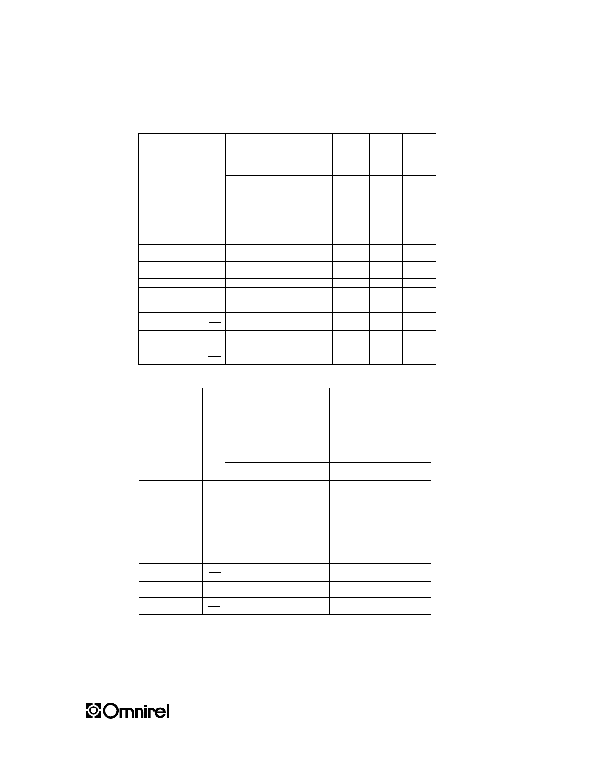
ELECTRICAL CHARACTERISTICS -5 V olt V
IN
= -10V, Io= 500mA, -55°C ≤ TA≤ 125°C (unless otherwise specified)
Parameter Symbol Test Conditions Min. Max. Unit
Output Voltage V
OUT
TA= 25°C -4.95 -5.05 V
V
IN
= -7.5V to -20V • -4.85 -5.15 V
Line Regulation V
RLINE
VIN= -7.5V to -20V 12 mV
(Note 1)
• 25 mV
V
IN
= -8.0V to -12V 5 mV
• 12 mV
Load Regulation V
RLOAD
IO = 5mA to 1.5 Amp 20 mV
(Note 1)
• 25 mV
I
O
= 250mA to 750 mA 15 mV
• 30 mV
Standby Current Drain I
SCD
2.5 mA
•
3.0 mA
Standby Current Drain ∆I
SCD
VIN= -7.0V to -20V
• 0.4 mA
Change With Line (Line)
Standby Current Drain ∆I
SCD
IO= 5mA to 1000mA • 0.4 mA
Change With Load (Load)
Dropout Voltage V
DO
∆V
OUT
= 100mV, I
O
= 1.0A • 2.5 V
Peak Output Current I
O (pk)
TA= 25°C 1.5 3.3 A
Short Circuit Current I
DS
VIN= -35V 1.2 A
(Note 2)
• 2.8 A
Ripple Rejection ∆V
IN
f =120 Hz, ∆VIN= -10V 63 dB
∆V
OUT
(Note 3) • 60 dB
Output Noise Voltage N
O
TA= 25°C, f =10 Hz to 100KHz 40 µV/V
(Note 3) RMS
Long Term Stability ∆V
OUT
TA= 25°C, t = 1000 hrs. 75 mV
(Note 3) ∆t
ELECTRICAL CHARACTERISTICS -12 Volt V
IN
= -19V, Io= 500mA, -55°C ≤ TA≤ 125°C (unless otherwise specified)
Parameter Symbol Test Conditions Min. Max. Unit
Output Voltage V
OUT
TA= 25°C -11.88 -12.12 V
V
IN
= -14.5V to -27V • -11.64 -12.36 V
Line Regulation V
RLINE
VIN= -14.5V to -27V 20 mV
(Note 1)
• 50 mV
V
IN
= -16V to -22V 10 mV
• 30 mV
Load Regulation V
RLOAD
IO = 5mA to 1.5 Amp 32 mV
(Note 1)
• 60 mV
I
O
= 250mA to 750 mA 16 mV
• 30 mV
Standby Current Drain I
SCD
3.5 mA
• 4.0 mA
Standby Current Drain ∆I
SCD
VIN= -14.5V to -27V • 0.8 mA
Change With Line (Line)
Standby Current Drain ∆I
SCD
IO= 5mA to 1000mA • 0.5 mA
Change With Load (Load)
Dropout Voltage V
DO
∆V
OUT
= 100mV, I
O
= 1.0A • 1.8 V
Peak Output Current I
O (pk)
TA= 25°C, IO= 5mA to 1A 1.5 3.3 A
Short Circuit Current I
DS
V
IN
= -35V 1.2 A
(Note 2)
• 2.8 A
Ripple Rejection ∆V
IN
f =120 Hz, ∆VIN= -10V 56 dB
∆V
OUT
(Note 3) • 53 dB
Output Noise Voltage N
O
TA= 25°C, f =10 Hz to 100KHz 40 µV/V
(Note 3) RMS
Long Term Stability ∆V
OUT
TA= 25°C, t = 1000 hrs. 120 mV
(Note 3) ∆t
Notes:
1. Load and Line Regulation are specified at a constant junction temperature. Pulse testing with low duty cycle is used.
Changes in output voltage due to heating effects must be taken into account separately.
2. Short Circuit protection is only assured up to V
IN
= -35V.
3. If not tested, shall be guaranteed to the specified limits.
4. The • denotes the specifications which apply over the full operating temperature range.
5. Refer to curves for typical characteristics versus Total Dose Radiation Levels.
OMR7905NH
OMR7912NH
OMR7915NH
OMR7905NM
OMR7912NM
OMR7915NM
OMR7905ST
OMR7912ST
OMR7915ST
OMR7905SR
OMR7912SR
OMR7915SR
RADIA TION TEST PROGRAM
The following chart is a summary of the test data collected on Radiation Tolerant
OMR7905/12/15 at various doses. The chart depicts the Total Radiation Dose that each device
was exposed to on a step stress irradiation basis prior to failure. Failure is defined as any
electrical test that does not meet the limits of the device per the published data sheet
specifications after radiation testing.
Omnirel P/N 5K 10K 20K 30K 50K 60K 70K 80K 100K 150K 200 250 300 350 400 450 KRAD
OMR7905/12/15
Test Points XX XX X X
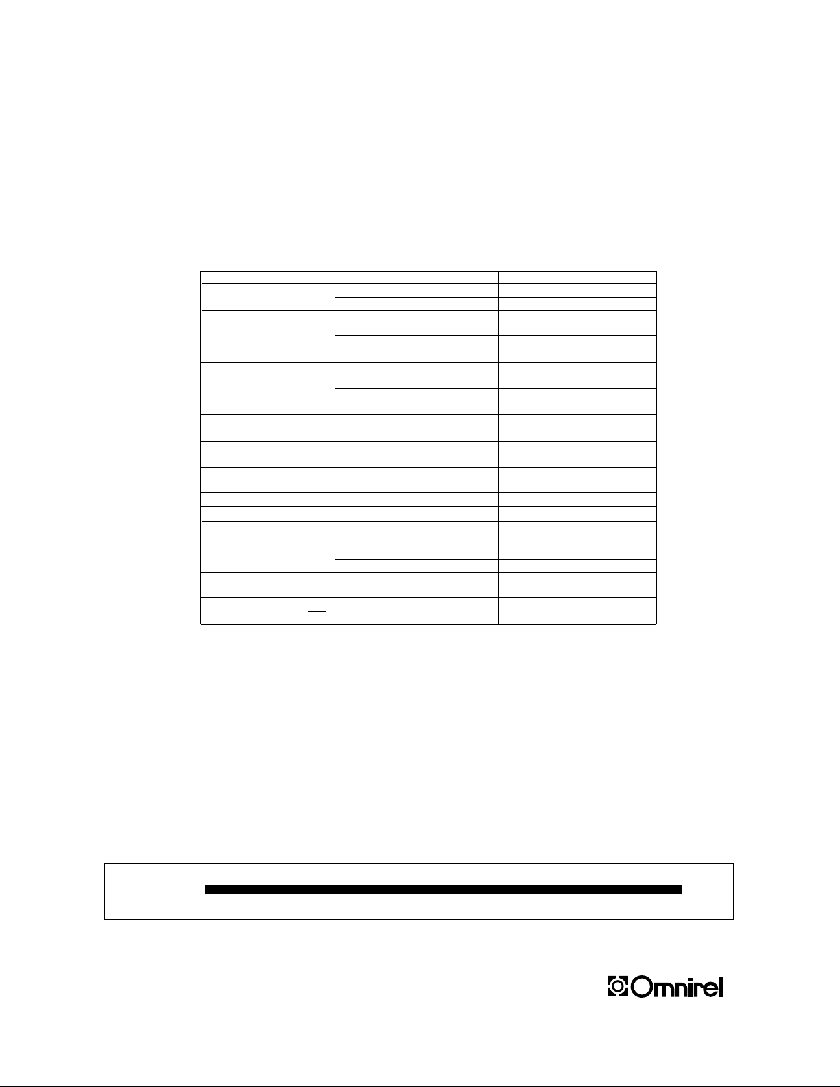
ELECTRICAL CHARACTERISTICS -15 Volt V
IN
= -23V, Io= 500mA, -55°C ≤ TA≤ 125°C (unless otherwise specified)
Parameter Symbol Test Conditions Min. Max. Unit
Output Voltage V
OUT
TA= 25°C -14.85 -15.15 V
V
IN
= -17.5V to -30V • -14.55 -15.45 V
Line Regulation V
RLINE
VIN= -17.5V to -30V 25 mV
(Note 1)
• 50 mV
V
IN
= -20V to -26V 15 mV
• 25 mV
Load Regulation V
RLOAD
IO = 5mA to 1.5 Amp 35 mV
(Note 1)
•
75 mV
I
O
= 250mA to 750 mA 21 mV
• 45 mV
Standby Current Drain I
SCD
6.0 mA
• 6.5 mA
Standby Current Drain ∆I
SCD
VIN= -17.5V to -30V • 0.8 mA
Change With Line (Line)
Standby Current Drain ∆I
SCD
IO= 5mA to 1000mA
• 0.5 mA
Change With Load (Load)
Dropout Voltage V
DO
∆V
OUT
= 100mV, I
O
= 1.0A • 2.5 V
Peak Output Current I
O (pk)
TA= 25°C 1.5 3.3 A
Short Circuit Current I
DS
VIN= -35V 1.2 A
(Note 2)
• 2.8 A
Ripple Rejection ∆V
IN
f =120 Hz, ∆VIN= -10V 53 dB
∆V
OUT
(Note 3)
• 50 dB
Output Noise Voltage N
O
TA= 25°C, f =10 Hz to 100KHz 40 µV/V
(Note 3) RMS
Long Term Stability ∆V
OUT
TA= 25°C, t = 1000 hrs. 150 mV
(Note 3) ∆t
Notes:
1. Load and Line Regulation are specified at a constant junction temperature. Pulse testing with low duty cycle is used.
Changes in output voltage due to heating effects must be taken into account separately.
2. Short Circuit protection is only assured up to V
IN
= -35V.
3. If not tested, shall be guaranteed to the specified limits.
4. The • denotes the specifications which apply over the full operating temperature range.
5. Refer to curves for typical characteristics versus Total Dose Radiation Levels.
OMR7905NH
OMR7912NH
OMR7915NH
OMR7905NM
OMR7912NM
OMR7915NM
OMR7905ST
OMR7912ST
OMR7915ST
OMR7905SR
OMR7912SR
OMR7915SR

• Radiation Testing is performed on a single wafer by wafer basis.
• Each wafer is identified and a random sample of 5 die per wafer is selected.
• The die are then individually assembled in a hermetic package, data logged, electrically
tested, hi-rel screened and then submitted to radiation testing.
• The packaged die are submitted to Steady State Total Dose radiation per Method 1019,
Condition A, at a dose rate of 50 RAD/sec biased at maximum supply voltage.
• Final electrical test is performed within two hours of both Total Dose Radiation level from
a Cobalt 60 source and 168 hr, 100°C annealing process. Read and record data
including two non-radiated control samples.
• The wafer is then qualified only if samples from wafers meet full electrical specifications
after 150% of total dose rating as specified in each product data sheet.
• Omnirel’s controlling specifications are as follows: For Voltage Regulators the
controlling specification is MIL-PRF- 38534/MIL-STD-883. For Rectifiers/Schottky the
controlling specification is MIL-PRF-19500/MIL-STD-750.
OMNIREL’S RADIATION TEST PROCEDURE
Standard Class Level Screening
Per MIL-PRF-38535
Screen *Level B *Level S
Test Method Required Test Method Required
Wafer Lot Acceptance ----- ----- 5007 100%
Non-destructive Bond Pull ----- ----- ----- ----Pre-Cap Visual Inspection 2010 100% 2010 100%
Temperature Cycle 1010 100% 1010 100%
Constant Acceleration 2001 100% 2001 100%
Visual Inspection ----- 100% ----- 100%
PIND Test ----- ----- 2020 100%
Serialization ----- ----- ----- 100%
Pre-Burn-In Electrical Data Sheet 100% Data Sheet 100%
Burn-In 1015/160 hrs. 100% 1015/240hrs. 100%
Interim Electrical ----- ----- Data Sheet 100%
PDA Calculations 5% Functional Lot 5% Functional Lot
Final Electrical Data Sheet 100% Data Sheet 100%
Fine & Gross Seal 1014 100% 1014 100%
Radiographic ----- ----- 2012/Two Views 100%
Conformance Inspection
** GR A 100% GR A 100%
Final Visual Inspection 2009 Sample 2009 Sample
* For “B” Level Screening add “M” to part number, for “S” Level Screening add “S” to part number.
See Part Number Designator.
** Additional conformance inspection testing, i.e. Group B, C, & D, optional.
AVAILABLE PRODUCT SCREENING
OMR7905NH
OMR7912NH
OMR7915NH
OMR7905NM
OMR7912NM
OMR7915NM
OMR7905ST
OMR7912ST
OMR7915ST
OMR7905SR
OMR7912SR
OMR7915SR

V
v
0
v
TYPICAL RADIATION CURVES
OMR7905NH
OMR7912NH
OMR7915NH
OMR7905NM
OMR7912NM
OMR7915NM
OMR7905ST
OMR7912ST
OMR7915ST
OMR7905SR
OMR7912SR
OMR7915SR
OMR7905STM
= 5ma to 1A
conditions: I
load
-4.850
-4.900
-4.950
-5.000
Vout (
-5.050
-5.100
-5.150
1 10 100 1000
OMR7905STM
conditions: Iload = -5ma to -1.5A
0.00
-4.00
-8.00
-12.00
Load Reg (m
-16.00
Typical Voltage Output
Radiation Total Dose (krads)
Typical Load Regulation
OMR7905STM
conditions: Vin = -10V
-3.300
-3.100
-2.900
-2.700
-2.500
Isc (
-2.300
-2.100
-1.900
-1.700
-1.500
1 10 100 1000
OMR7905STM
conditions: Vin = -7.5V to -20v
12.00
10.00
8.00
6.00
Line Reg (m
4.00
2.00
Typical Short Circuit Current
Radiation Total Dose (krads)
Typical Line Regulation
-20.00
1 10 100 1000
Radiation Total Dose (krads)
0.00
1 10 100 100
Radiation Total Dose (krads)

-11.880
V
v
v
TYPICAL RADIATION CURVES
OMR7905NH
OMR7912NH
OMR7915NH
OMR7905NM
OMR7912NM
OMR7915NM
OMR7905ST
OMR7912ST
OMR7915ST
OMR7905SR
OMR7912SR
OMR7915SR
V
v
v
-11.920
-11.960
-12.000
Vout (
-12.040
-12.080
OMR7912STM
conditions: I
load
= 5ma to 1A
Typical Voltage Output
10.00
8.00
6.00
4.00
Line Reg (m
2.00
OMR7912STM
conditions: Vin = -14.5V to -27v
Typical Line regulation
-12.120
1 10 100 1000
OMR7912STM
conditions: Vin = -35V
-0.200
-0.300
-0.400
-0.500
-0.600
-0.700
Isc (
-0.800
-0.900
-1.000
-1.100
-1.200
1 10 100 1000
OMR7915STM
= 5ma to 1A
conditions: I
load
-14.850
-14.900
-14.950
-15.000
Vout (
-15.050
-15.100
-15.150
1 10 100 1000
Radiation Total Dose (krads)
Typical Short Circuit Current
Radiation Total Dose (krads)
Typical Voltage Output
Radiation Total Dose (krads)
OMR7915STM
conditions: Vin = -17.5V to -30v
25.00
20.00
15.00
10.00
Line Reg (m
5.00
0.00
1 10 100 1000
Typical Line Regulation
Radiation Total Dose (krads)
0.00
1 10 100 1000
OMR7912STM
= 5ma to 1.5A
conditions: I
load
0.00
-1.00
-2.00
-3.00
-4.00
-5.00
-6.00
Load Reg (m
-7.00
-8.00
-9.00
-10.00
1 10 100 1000
OMR7915STM
= 5ma to 1.5A
conditions: I
load
0.00
-2.00
-4.00
-6.00
Load Reg (m
-8.00
-10.00
-12.00
1 10 100 1000
OMR7915STM
conditions: Vin = -35V
-0.500
-0.505
-0.510
-0.515
-0.520
Isc (
-0.525
-0.530
-0.535
-0.540
1 10 100 1000
Radiation Total Dose (krads)
Typical Load Regulation
Radiation Total Dose (krads)
Typical Load Regulation
Radiation Total Dose (krads)
Typical Short Circuit Current
Radiation Total Dose (krads)

OMR7905NH
OMR7912NH
OMR7915NH
OMR7905NM
OMR7912NM
OMR7915NM
OMR7905ST
OMR7912ST
OMR7915ST
OMR7905SR
OMR7912SR
OMR7915SR
3.5
3
2.5
2
1.5
1
0.5
0
0 5 10 15 20 25 30 35
PEAK OUTPUT CURRENT
∆V
OUT
= 100mV
T
j
= -55°C
T
j
= 25°C
T
j
= 150°C
Input To Output Differential (V)
2.5
2
1.5
1
0.5
0
-75 -50 -25 0 25 50 75 100 125 150
DROPOUT VOLTAGE
∆V
OUT
= 100MV
I
OUT
= 0A
I
OUT
= 500mA
I
OUT
= 1A
Junction T emper ature (°C)
100
80
60
40
20
0
10 100 1k 10k 100k
RIPPLE REJECTION
V
OUT
= 5V
V
IN
- V = 8V
DC
+3.5V
rms
I
OUT
= 1A
T
j
= 25°C
Frequency (Hz)
TYPICAL PERFORMANCE CHARACTERISTICS
TYPICAL APPLICATIONS
Basic Current Regulator Fixed Output Regulator
V
IN
V
OUT
1µF2.2µF
OM79XX
++
V
IN
I
OUT
2.2µF
R1
OM79XX
I
Q
I
OUT
=
V
OUT
R1
+ I
Q
Input bypass capacitors are recommended for stable operation of the OM7900 series of regulators over the
input voltage and output current ranges. Output bypass capacitors will improve the transient response of the
regulator.
The bypass capacitors, (2.2µF on the input, 1µF on the output) should be ceramic or solid tantalum which
have good high frequency characteristics. If aluminum electrolytics are used, their values should be 10µF or
larger. The bypass capacitors should be mounted with the shortest leads, and if possible, directly across the
regulator terminals.

MECHANICAL OUTLINES
205 Crawford Street, Leominster, MA 01453 USA (978) 534-5776 FAX (978) 537-4246
Visit Our Web Site at www.omnirel.com
OMR79XXNH
Non-Isolated
Pin 1 - Ground
Pin 2 - Output
Pin 3 - Input(Case)
Add “H” to part number for TO-205 Package
OMR79XXST
Isolated/Front View
Pin 1 - Ground
Pin 2 - Input
Pin 3 - Output
Tab - Isolated
Add “T” to part number for
TO-257 Package
OMR79XXNM
Pin 1 - Ground
Pin 2 - Output
Pin 3 - Input
Add “M” to part number for
SMD (Surface Mount Package)
.430
.410
.200
.190
.038 MAX.
.005
.120 TYP.
.537
.527
.665
.645
.420
.410
.150
.140
.750
.500
.100 TYP.
.035
.025
.045
.035
.450
.140
.415
.157
.015
.140
.140
.050
.050
.037
.375
.030
MIN.
TOP VIEW SIDE VIEW BOTTOM VIEW
.625
123
1
2
3
“T” P/N DESIGNATOR
“H” P/N DESIGNATOR
TO-257AA
TO-205AF (TO-39)
SMD-1
PART NUMBER DESIGNATOR
(Example OMR7905STM
OMR 7905 S T M
Omnirel Device Isolated Package Screening
Rad-Tolerant Type Package Style Level
Hermetic D2Pac
“R” P/N DESIGNATOR
OMR79XXSR
Isolated
Front View
Pin 1 - Ground
Pin 2 - Input
Pin 3 - Output
Tab - Isolated
Add “R” to part number for
D2Pac Package
“M” P/N DESIGNATOR
OMR7905NH
OMR7912NH
OMR7915NH
OMR7905NM
OMR7912NM
OMR7915NM
OMR7905ST
OMR7912ST
OMR7915ST
OMR7905SR
OMR7912SR
OMR7915SR
123
 Loading...