

Page 1
3.3 - 1
3.3
Three T erminal, Fixed V oltage, 1.5 Amp
Precision Negative Regulators In Hermetic
JEDEC TO-257AA Package and D
2
Pac
0 03 R5
Supersedes 4 11 R4
ISOLATED HERMETIC TO-257AA FIXED
VOLTAGE NEGATIVE REGULATORS
FEATURES
• Isolated Hermetic Package, JEDEC TO-257AA Outline
• Output Voltages: -5V, -12V, -15V (Other Voltages Available)
• Output Voltages Set Internally To ±1% or ±2%
• Built-In Thermal Ov erload Protection
• Short Circuit Current Limiting
• Product Is Available Screened To MIL-STD-883
DESCRIPTION
These three terminal negative regulators are supplied in a hermetically sealed
metal package whose outline is similar to the industry standard TO-220 plastic package. All protective features are designed into the circuit, including thermal shutdown,
current limiting and safe-area control. With heat sinking, they can deliver over 1.5
amps of output current. These units feature internally trimmed output voltages to ±1%
or 2% of nominal voltage. Standard voltages are -5V, -12V, and
-15V. However, other voltages are available up to -24 volts. These units are ideally
suited for Military applications where a hermetically sealed package is required.
ABSOLUTE MAXIMUM RATINGS @ 25°C
Input V oltage ................................................................. -35 V
Operating Junction Temperature Range .......................... - 55°C to + 150°C
Storage Temperature Range ..................................... - 65°C to + 150°C
Typical Power/Thermal Characteristics:
Rated Power @ 25° C TC.............................................. 17.5W
TA................................................. 3W
Thermal Resistance
θ
JC
............................................4.2°C/W
θ
JA
............................................ 42°C/W
OM7900IH Series
OM7900SR Series
Notes: Product also available in Non-Isolated construction. To order this version,
delete “I” from part number.
Example: Isolated
Non-Isolated
OM79XXIH OM79XXH
Use letter “A” after part number to designate ±1% output voltage tolerance.
Example: OM7905AIH
Page 2
3.3 - 2
3.3
OM7900IH
OM7900SR
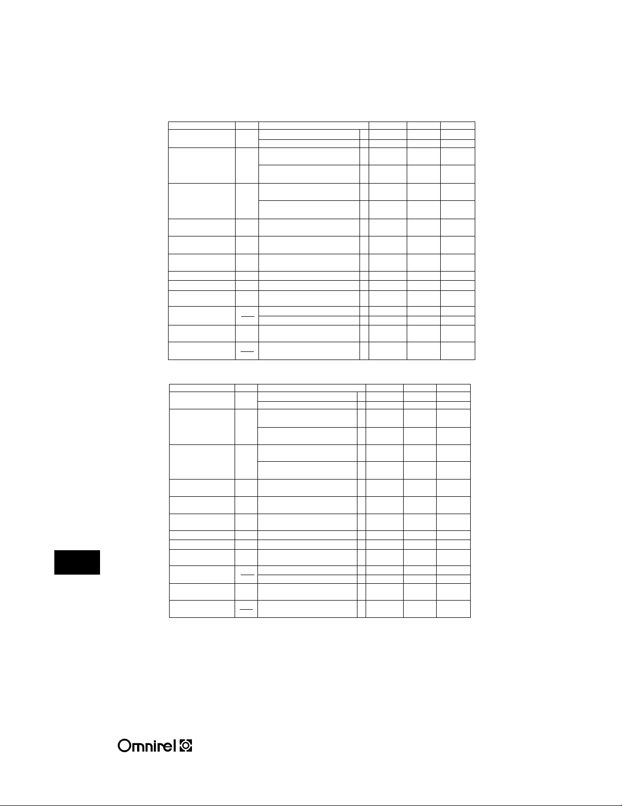
ELECTRICAL CHARACTERISTICS -5 V olt V
IN
= -10V, Io= 500mA, -55°C ≤ TA≤ 125°C (unless otherwise specified)
Parameter Symbol Test Conditions Min. Max. Unit
Output Voltage V
OUT
TA= 25°C -4.95 -5.05 V
V
IN
= -7.5V to -20V • -4.85 -5.15 V
Line Regulation V
RLINE
VIN= -7.5V to -20V 12 mV
(Note 1)
• 25 mV
V
IN
= -8.0V to -12V 5 mV
• 12 mV
Load Regulation V
RLOAD
IO = 5mA to 1.5 Amp 20 mV
(Note 1)
• 25 mV
I
O
= 250mA to 750 mA 15 mV
• 30 mV
Standby Current Drain I
SCD
2.5 mA
• 3.0 mA
Standby Current Drain ∆I
SCD
VIN= -7.0V to -20V
• 0.4 mA
Change With Line (Line)
Standby Current Drain ∆I
SCD
IO= 5mA to 1000mA • 0.4 mA
Change With Load (Load)
Dropout Voltage V
DO
∆V
OUT
= 100mV, I
O
= 1.0A • 2.5 V
Peak Output Current I
O (pk)
TA= 25°C 1.5 3.3 A
Short Circuit Current I
DS
VIN= -35V 1.2 A
(Note 2)
• 2.8 A
Ripple Rejection ∆V
IN
f =120 Hz, ∆VIN= -10V 63 dB
∆V
OUT
(Note 3) • 60 dB
Output Noise Voltage N
O
TA= 25°C, f =10 Hz to 100KHz 40 µV/V
(Note 3) RMS
Long Term Stability ∆V
OUT
TA= 25°C, t = 1000 hrs. 75 mV
(Note 3) ∆t
ELECTRICAL CHARACTERISTICS -12 Volt V
IN
= -19V, Io= 500mA, -55°C ≤ TA≤ 125°C (unless otherwise specified)
Parameter Symbol Test Conditions Min. Max. Unit
Output Voltage V
OUT
TA= 25°C -11.88 -12.12 V
V
IN
= -14.5V to -27V • -11.64 -12.36 V
Line Regulation V
RLINE
VIN= -14.5V to -27V 20 mV
(Note 1)
• 50 mV
V
IN
= -16V to -22V 10 mV
• 30 mV
Load Regulation V
RLOAD
IO = 5mA to 1.5 Amp 32 mV
(Note 1)
• 60 mV
I
O
= 250mA to 750 mA 16 mV
•
30 mV
Standby Current Drain I
SCD
3.5 mA
• 4.0 mA
Standby Current Drain ∆I
SCD
VIN= -14.5V to -27V • 0.8 mA
Change With Line (Line)
Standby Current Drain ∆I
SCD
IO= 5mA to 1000mA • 0.5 mA
Change With Load (Load)
Dropout Voltage V
DO
∆V
OUT
= 100mV, I
O
= 1.0A • 1.8 V
Peak Output Current I
O (pk)
TA= 25°C, IO= 5mA to 1A 1.5 3.3 A
Short Circuit Current I
DS
V
IN
= -35V 1.2 A
(Note 2)
• 2.8 A
Ripple Rejection ∆V
IN
f =120 Hz, ∆VIN= -10V 56 dB
∆V
OUT
(Note 3) • 53 dB
Output Noise Voltage N
O
TA= 25°C, f =10 Hz to 100KHz 40 µV/V
(Note 3) RMS
Long Term Stability ∆V
OUT
TA= 25°C, t = 1000 hrs. 120 mV
(Note 3) ∆t
Notes:
1. Load and Line Regulation are specified at a constant junction temperature. Pulse testing with low duty cycle is used.
Changes in output voltage due to heating effects must be taken into account separately.
2. Short Circuit protection is only assured up to V
IN
= -35V.
3. If not tested, shall be guaranteed to the specified limits.
The • denotes the specifications which apply over the full operating temperature range.
Page 3
3.3 - 3
3.3
OM7900IH Series
OM7900SR Series
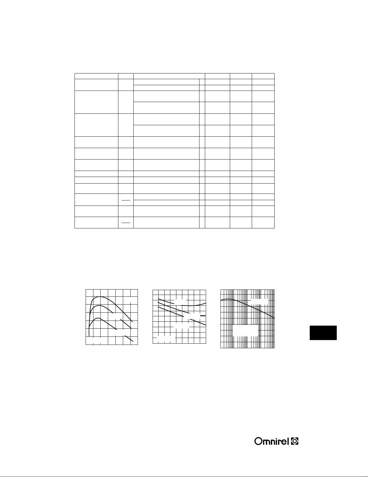
ELECTRICAL CHARACTERISTICS -15 Volt V
IN
= -23V, Io= 500mA, -55°C ≤ TA≤ 125°C (unless otherwise specified)
Parameter Symbol Test Conditions Min. Max. Unit
Output Voltage V
OUT
TA= 25°C -14.85 -15.15 V
V
IN
= -17.5V to -30V • -14.55 -15.45 V
Line Regulation V
RLINE
VIN= -17.5V to -30V 25 mV
(Note 1)
• 50 mV
V
IN
= -20V to -26V 15 mV
• 25 mV
Load Regulation V
RLOAD
IO = 5mA to 1.5 Amp 35 mV
(Note 1)
•
75 mV
I
O
= 250mA to 750 mA 21 mV
• 45 mV
Standby Current Drain I
SCD
6.0 mA
• 6.5 mA
Standby Current Drain ∆I
SCD
VIN= -17.5V to -30V
• 0.8 mA
Change With Line (Line)
Standby Current Drain ∆I
SCD
IO= 5mA to 1000mA • 0.5 mA
Change With Load (Load)
Dropout Voltage V
DO
∆V
OUT
= 100mV, I
O
= 1.0A • 2.5 V
Peak Output Current I
O (pk)
TA= 25°C 1.5 3.3 A
Short Circuit Current I
DS
VIN= -35V 1.2 A
(Note 2)
• 2.8 A
Ripple Rejection ∆V
IN
f =120 Hz, ∆VIN= -10V 53 dB
∆V
OUT
(Note 3) • 50 dB
Output Noise Voltage N
O
TA= 25°C, f =10 Hz to 100KHz 40 µV/V
(Note 3) RMS
Long Term Stability ∆V
OUT
TA= 25°C, t = 1000 hrs. 150 mV
(Note 3) ∆t
Notes:
1. Load and Line Regulation are specified at a constant junction temperature. Pulse testing with low duty cycle is used.
Changes in output voltage due to heating effects must be taken into account separately.
2. Short Circuit protection is only assured up to V
IN
= -35V.
3. If not tested, shall be guaranteed to the specified limits.
The • denotes the specifications which apply over the full operating temperature range.
3.5
3
2.5
2
1.5
1
0.5
0
0510
PEAK OUTPUT CURRENT
∆V
OUT
= 100mV
Tj= -55°C
Tj= 25°C
Tj= 150°C
Input To Output Differential (V)
2.5
2
1.5
1
0.5
0
-75 -50 -25 0 25 50 75 100 125 150
DROPOUT VOLTAGE
∆V
OUT
= 100MV
I
OUT
= 0A
I
OUT
= 500mA
I
OUT
= 1A
Junction T emper ature (°C)
100
80
60
40
20
0
10 100 1k 10k 100k
RIPPLE REJECTION
V
OUT
= 5V
V
IN
- V = 8V
DC
+3.5V
rms
I
OUT
= 1A
T
j
= 25°C
Frequency (Hz)
TYPICAL PERFORMANCE CHARACTERISTICS
Page 4
3.3
OM7900IH Series
OM7900SR Series
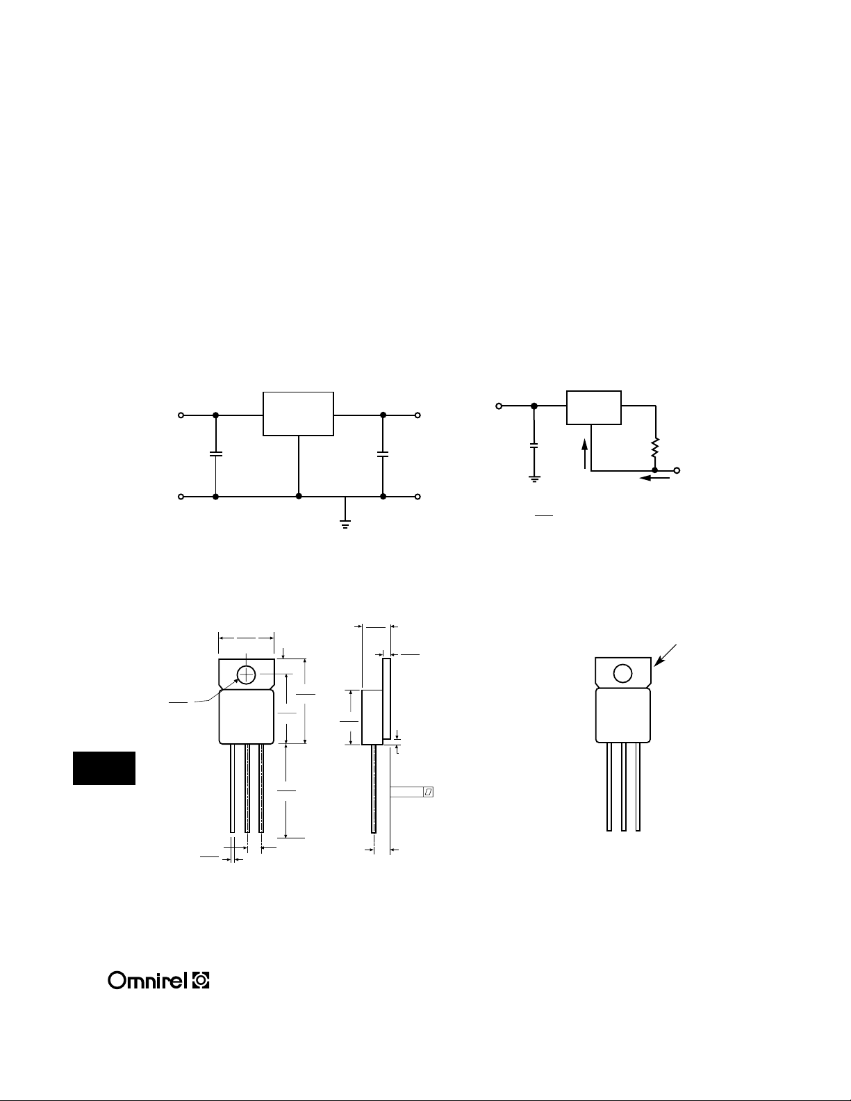
TYPICAL APPLICATIONS
MECHANICAL OUTLINE PIN CONNECTION
Fixed Output Regulator Basic Current Regulator
.430
.410
.200
.190
.038 MAX.
.005
.120 TYP.
.537
.527
.665
.645
.420
.410
.150
.140
.750
.500
.100 TYP.
.035
.025
.045
.035
123
Note:
• Case is metal/her metically sealed
• Isolated Tab
• Outline similar to JEDEC TO-220 outline
OM79XXIH
Isolated
Front View
Pin 1: Ground
Pin 2: Input
Pin 3: Output
Tab: Isolated
OM79XXH
Non-Isolated
Front View
Pin 1: Ground
Pin 2: Input
Pin 3: Output
Tab Input
Tab
V
IN
V
OUT
1µF2.2µF
1
23
OM79XX
++
V
IN
I
OUT
2
1
3
2.2µF
R1
OM79XX
I
Q
I
OUT
=
V
OUT
R1
+ I
Q
Input bypass capacitors are recommended for stable operation of the OM7900 series of regulators over
the input voltage and output current ranges. Output bypass capacitors will improve the transient response
of the regulator.
The bypass capacitors, (2.2µF on the input, 1µF on the output) should be ceramic or solid tantalum which
have good high frequency characteristics. If aluminum electrolytics are used, their values should be 10µF
or larger. The bypass capacitors should be mounted with the shortest leads, and if possible, directly
across the regulator terminals.
Page 5
OM 7900 S R M
Omnirel Device Isolated Package Hi-Rel Screening
Type Package Style Level
PART NUMBER DESIGNATOR
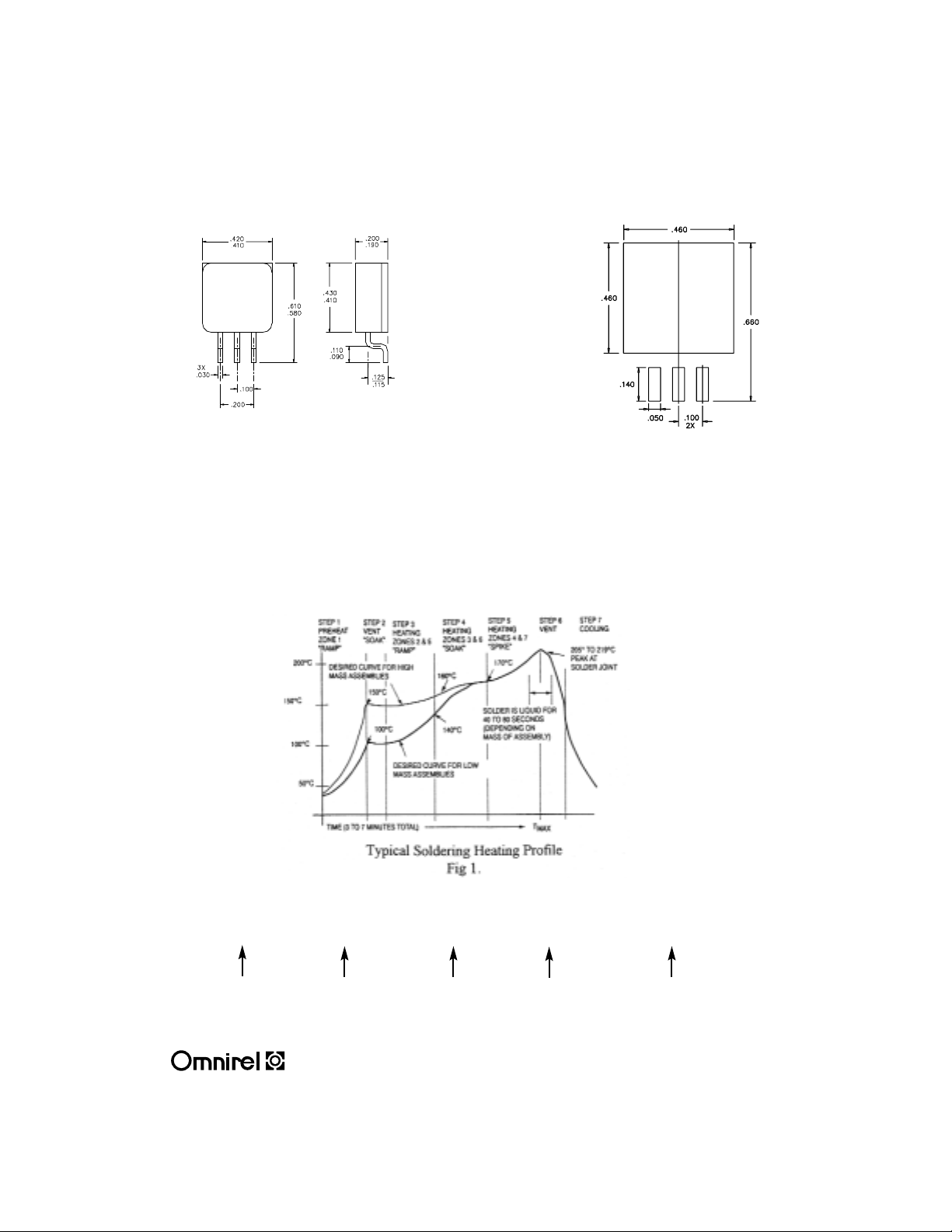
Figure 1 shows a typical soldering profile for the D2and D3Packages when soldering a to a printed circuit board.The
profile will vary from system to system and solders to solders. Factors that can affect the profile include the type of soldering system used, density and type of components on the board or substrate material being used.This profile shows
temperature versus time.The two profiles described are based on a high density and a low density board.The type solder used was 62/36/2 Tin Lead Silver with a melting point between 177-189ºC.An convection/infrared soldering reflow
system was used.The circuit and solder joints heat up first due to their mass followed by the components which typically run 30 degrees cooler than the solder joints.
TYPICAL HEATING PROFILE
TYPICAL SOLDERING PROFILE
MECHANICAL OUTLINE SOLDERING FOOTPRINT
Pin 1: Ground
Pin 2: Input
Pin 3: Output
Case N/C
205 Crawford Street, Leominster, MA 01453 USA (508) 534-5776 FAX (508) 537-4246
OM7900IH Series
OM7900SR Series
12 3
 Loading...