

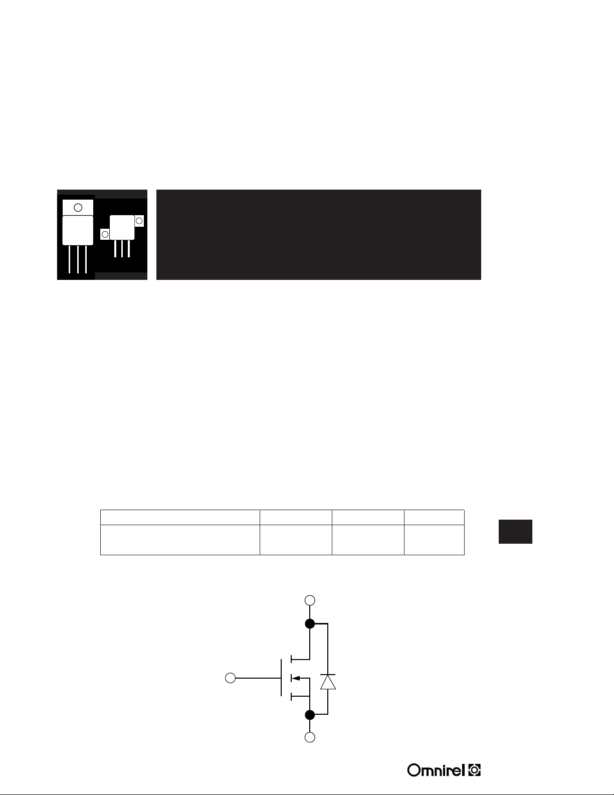
POWER MOSFET IN HERMETIC ISOLATED
DRAIN
GATE
SOURCE
TO-254AA PACKAGE
600V & 550V, 11 Amp, N-Channel
MOSFET In Hermetic Metal Package
FEATURES
• Isolated Hermetic Metal Package
• Fast Switching
• Low R
• Available Screened To MIL-S-19500, TX, TXV And S
• Ceramic Feedthroughs Also Available
DESCRIPTION
This series of hermetically packaged products feature the latest advanced MOSFET
and packaging technology. The device breakdown ratings provide a substantial
voltage margin for stringent applications such as 270 VDC aircraft power and/or
rectified 230 VAC power (line operation). They are ideally suited for Military
requirements where small size, high performance and high reliability are required,
and in applications such as switching power supplies, motor controls, inverters,
choppers, audio amplifiers and high energy pulse circuits.
DS(on)
OM11N60SA
OM11N55SA
4 11 R1
Supersedes 2 04 R0
MAXIMUM RATINGS
PART NUMBER V
OM11N60 600V .50 11A
OM11N55 550V .44 11A
DS
SCHEMATIC
3.1 - 19
R
DS(on)
I
D(MAX)
3.1
3.1
G
D
S
G
D
S
OM11N60SA - OM11N55SA
ELECTRICAL CHARACTERISTICS: T
= 25° unless otherwise noted ELECTRICAL CHARACTERISTICS: TC= 25° unless otherwise noted
C
STATIC P/N OM11N60SA STATIC P/N OM11N55SA
Parameter Min. Typ. Max. Units Test Conditions Parameter Min. Typ. Max. Units Test Conditions
BV
Drain-Source Breakdown 600 V VGS= 0, BV
DSS
Voltage I
V
Gate-Threshold Voltage 2.0 4.0 V VDS= VGS, ID= 250 mAV
GS(th)
I
Gate-Body Leakage ± 100 nA VGS= ± 20 V I
GSS
I
Zero Gate Voltage Drain 0.1 0.25 mA VDS= Max. Rat., VGS= 0 I
DSS
Current 0.2 1.0 mA V
I
On-State Drain Current
D(on)
V
Static Drain-Source On-State 3.1 V VGS= 10 V, ID= 5.5 A V
DS(on)
R
DS(on)
R
DS(on)
3.1 - 20
DYNAMIC DYNAMIC
g
fs
C
iss
C
oss
C
rss
T
d(on)
t
r
T
d(off)
t
f
1
Voltage
Static Drain-Source On-State .47 .50 VGS= 10 V, ID= 5.5 A R
Resistance
1
Static Drain-Source On-State 1.0 VGS= 10 V, ID= 5.5 A, R
Resistance
1
Forward Transductance
Input Capacitance 3000 pF VGS= 0 C
Output Capacitance 440 pF VDS= 25 V C
Reverse Transfer Capacitance 220 pF f = 1 MHz C
Turn-On Delay Time 55 ns VDD= 210 V, ID@ 7.0 A T
Rise Time 75 ns Rg= 5 W, RL= 30 W t
Turn-Off Delay Time 225 ns T
Fall Time 135 ns t
1
11.0 A VDS> I
1
5.0 S(W) VDS 2 V
= 250 mA Voltage ID= 250 mA
D
= 0.8 Max. Rat., VGS= 0, Current 0.2 1.0 mA VDS= 0.8 Max. Rat., VGS= 0,
DS
T
= 125° C TC= 125° C
C
x R
D(on)
, VGS= 10 V I
DS(on)
TC= 125 C Resistance
(W)(W)
(MOSFET) switching times are
essentially independent of
operating temperature.
, ID= 5.5 A g
DS(on)
BODY-DRAIN DIODE RATINGS AND CHARACTERISTICS BODY-DRAIN DIODE RATINGS AND CHARACTERISTICS
I
Continuous Source Current - 11 A Modified MOSPOWER I
S
(Body Diode) symbol showing (Body Diode) symbol showing
I
Source Current
SM
(Body Diode) Junction rectifier. (Body Diode) Junction rectifier.
VSDDiode Forward Voltage
t
Reverse Recovery Time 700 ns TJ= 150 C,IF= IS,t
rr
1 Pulse Test: Pulse Width 300msec, Duty Cycle 2%. 1 Pulse Test: Pulse Width 300msec, Duty Cycle 2%.
1
1
- 52 A the integral P-N I
- 1.4 V TC= 25 C, IS= -11 A, VGS= 0 VSDDiode Forward Voltage
dl
/ds = 100 A/ms dlF/ds = 100 A/ms
F
Drain-Source Breakdown 550 V VGS= 0,
DSS
Gate-Threshold Voltage 2.0 4.0 V VDS= V
GS(th)
Gate-Body Leakage Forward ±100 nA VGS= ± 20 V
GSSF
Zero Gate Voltage Drain 0.1 0.25 mA VDS= Max. Rat., VGS= 0
DSS
On-State Drain Current
D(on)
Static Drain-Source On-State 3.3 V VGS= 10 V, ID= 5.5 A
DS(on)
DS(on)
DS(on)
fs
iss
oss
rss
d(on)
r
d(off)
f
S
SM
rr
1
Voltage
Static Drain-Source On-State .37 .44 VGS= 10 V, ID= 5.5 A
Resistance
1
Static Drain-Source On-State .88 VGS= 10 V, ID= 5.5 A,
1
Forward Transductance
Input Capacitance 3000 pF VGS= 0
Output Capacitance 440 pF VDS= 25 V
Reverse Transfer Capacitance 220 pF f = 1 MHz
Turn-On Delay Time 55 ns VDD= 210 V, ID@ 7.0 A
Rise Time 75 ns Rg= 5 W, RL= 30 W
Turn-Off Delay Time 225 ns
Fall Time 135 ns
Continuous Source Current - 11 A Modified MOSPOWER
Source Current
Reverse Recovery Time 700 ns TJ= 150 C,IF= IS,
1
1
1
1
11.0 A VDS> I
5.0 S(W) VDS 2 V
- 52 A the integral P-N
- 1.4 V TC= 25 C, IS= -11 A, VGS= 0
, I
= 250 mA
GS
D
x R
D(on)
, VGS= 10 V
DS(on)
TC= 125 C
, ID= 5.5 A
DS(on)
(MOSFET) switching times are
essentially independent of
operating temperature.

OM11N60SA - OM11N55SA
ABSOLUTE MAXIMUM RATINGS (TC= 25°C unless otherwise noted)
Symbol Parameter OM11N60 OM11N55 Units
V
DGR
V
DS
I
D
I
D
I
DM
P
D
P
D
Drain Source Voltage 600 550 V
Drain Gate Voltage (RGS= 1.0 M ) 600 550 V
Continuous Drain Current @ TC= 25°C 11 11 A
Continuous Drain Current @ TC= 100°C 7.2 7.2 A
Pulsed Drain Current
1
52 52 A
Max. Power Dissipation @ TC= 25°C 125 125 W
Max. Power Dissipation @ TC= 100°C 50 50 W
Linear Derating Factor Jct. to Case 1.0 1.0 W/°C
Linear Derating Factor Jct. to Ambient .020 .020 W/°C
TJ, T
stg
Operating and Storage Temp. Range -55 to 150 °C
Lead Temperature (1/16" from case for 10 sec.) 300 300 °C
1 Pulse Test: Pulse width 300 µsec. Duty Cycle 2%.
THERMAL RESISTANCE (Maximum at TA= 25°C)
R
thJC
R
thJA
Junction-to-Case 1.0 1.0 °C/W
Junction-to-Ambient (Free Air Operation) 50 50 °C/W
3.1 - 21
3.1

OM11N60SA - OM11N55SA
205 Crawford Street, Leominster, MA 01 453 USA (508) 534-5776 FAX (508) 537-4246
.144 DIA.
.050
.040
.260
.249
.685
.665
.800
.790
.545
.535
.550
.510
.045
.035
.550
.530
.150 TYP.
.150 TYP.
.005
.040 DIA.
3 PLCS.
.150
.260
MAX
.040
.940
.500
MIN.
.150
.125
2 PLCS.
.290
.125 DIA.
2 PLS.
.200
.540
.250
.740
.540
.100
2 PLCS.
.300
MECHANICAL OUTLINES
TO-254 AA Package
3.1
Standard Products are supplied with glass feedthroughs, for ceramic feedthroughs, add letter “C” to part number,
For Z-Pack configuration, add letter “Z” to part number, Example - OMXXXXSAZ
Omnirel AZ Package
Example - OMXXXXCSA
 Loading...