

Page 1
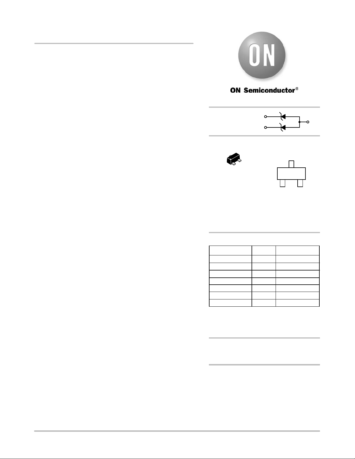
NZL5V6AXV3T1 Series
l
Preferred Devices
Dual Common Anode
ESD Protection Diodes
SC−89 Package
These dual monolithic silicon ESD protection diodes are intended for
use in voltage− and ESD−sensitive equipment such as computers,
printers, business machines, communication systems, medical
equipment and other applications. Their dual junction common anode
design protects two separate lines using only one package. These
devices are ideal for situations where board space is at a premium.
Specification Features:
• SC−89 Package Allows Either Two Separate Unidirectional
Configurations or a Single Bidirectional Configuration
• ESD Rating of Class N (exceeding 16 kV) per the
Human Body Model
• Meets IEC61000−4−2 Level 4
• Low Leakage < 5.0 mA
• These are Pb−Free Devices
Mechanical Characteristics:
Void-free, Transfer-molded, Thermosetting Plastic
CASE:
Epoxy Meets UL 94, V−0
LEAD FINISH: 100% Matte Sn (Tin)
MOUNTING POSITION: Any
QUALIFIED MAX REFLOW TEMPERATURE:
260°C Device Meets MSL 1 Requirements
http://onsemi.com
PIN 1. CATHODE
2. CATHODE
3. ANODE
1
3
2
MARKING
DIAGRAM
3
1
Lx G
G
2
M
SC−89
CASE 463C
STYLE 4
L = Device Code
x = Specific Device
M = Date Code
G = Pb−Free Package
(Note: Microdot may be in either location)
ORDERING INFORMATION
Device Package Shipping
NZL5V6AXV3T1 SC−89* 3000/Tape & Reel
NZL5V6AXV3T1G SC−89* 3000/Tape & Reel
NZL6V8AXV3T1 SC−89*
NZL6V8AXV3T3G SC−89*
NZL7V5AXV3T1
NZL7V5AXV3T1G SC−89*
†For information on tape and reel specifications,
including part orientation and tape sizes, please
refer to our Tape and Reel Packaging Specification
Brochure, BRD8011/D.
*This package is inherently Pb−Free.
SC−89*
3000/Tape & Reel
3000/Tape & ReelNZL6V8AXV3T1G SC−89*
10000/Tape & Ree
3000/Tape & Reel
3000/Tape & Reel
†
DEVICE MARKING INFORMATION
See specific marking information in the device marking
column of the table on page 2 of this data sheet.
© Semiconductor Components Industries, LLC, 2007
February, 2007 − Rev. 5
Preferred devices are recommended choices for future use
and best overall value.
1 Publication Order Number:
NZL5V6AXV3T1/D
Page 2
NZL5V6AXV3T1 Series
MAXIMUM RATINGS
Rating Symbol Value Unit
Total Power Dissipation on FR−5 Board (Note 1) @ TA = 25°C
Derate above 25°C
Thermal Resistance Junction to Ambient
Junction and Storage Temperature Range TJ, T
Lead Solder Temperature − Maximum (10 Second Duration) T
IEC61000−4−2 (Contact) 10 kV
Stresses exceeding Maximum Ratings may damage the device. Maximum Ratings are stress ratings only. Functional operation above the
Recommended Operating Conditions is not implied. Extended exposure to stresses above the Recommended Operating Conditions may affect
device reliability.
1. FR−5 board with minimum recommended mounting pad.
*Other voltages may be available upon request.
°PD° 240
1.9
R
q
JA
stg
L
525 °C/W
−55 to +150 °C
260 °C
°mW°
mW/°C
ELECTRICAL CHARACTERISTICS
(TA = 25°C unless otherwise noted)
UNIDIRECTIONAL (Circuit tied to Pins 1 and 3 or 2 and 3)
I
I
F
Symbol Parameter
V
RWM
I
V
I
I
V
Working Peak Reverse Voltage
Maximum Reverse Leakage Current @ V
R
Breakdown Voltage @ I
BR
Test Current
T
Forward Current
F
Forward Voltage @ I
F
F
RWM
T
VCV
BR
V
RWM
I
V
R
F
I
T
I
PP
V
Uni−Directional TVS
ELECTRICAL CHARACTERISTICS (T
= 25°C unless otherwise noted, VF = 0.9 V Max @ IF = 10 mA for all types)
A
UNIDIRECTIONAL (Circuit tied to Pins 1 and 3 or Pins 2 and 3)
Breakdown Voltage Surge
VC (V) @
T
IPP = 1.0
A
Device
Device
Marking
V
RWM
V
IR @
V
RWM
mA
V
(Note 2) (V) @ Iz
BR
Min Nom Max mA Typ Max Typ
NZL5V6AXV3T1 L0 3.0 5.0 5.32 5.6 5.88 5.0 7.0 10.1 4.8 50
NZL6V8AXV3T1 L2 4.5 1.0 6.46 6.8 7.14 5.0 7.9 11.9 6.7 73
NZL6V8AXV3T3 L2 4.5 1.0 6.46 6.8 7.14 5.0 7.9 11.9 6.7 73
NZL7V5AXV3T1 L3 5.0 1.0 7.12 7.5 7.88 5.0 8.8 13.5 5.7 75
2. VBR measured at pulse test current IT at an ambient temperature of 25°C.
† Surge current waveform per Figure 5.
VC (V) @
†
Max I
PP
Max I
PP
(A)
†
†
P
(W)
pk
†
http://onsemi.com
2
Page 3
NZL5V6AXV3T1 Series
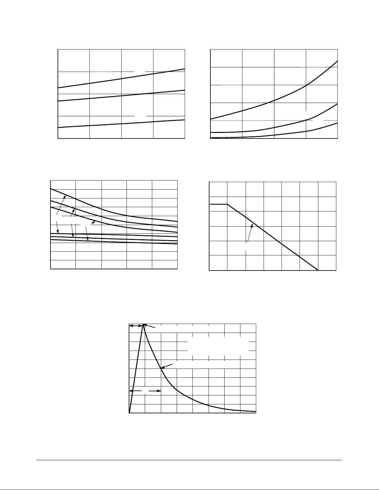
BREAKDOWN VOLTAGE (VOLTS) (V
@ I
)
5
CAPACITANCE (pF)
TYPICAL CHARACTERISTICS
T
9.0
250
BR
8.0
7.0
6.0
5.0
−55 +45
−5
TEMPERATURE (°C)
7V5
6V8
5V6
+95 +145
Figure 1. Typical Breakdown Voltage
versus Temperature
50
45
40
35
30
5V6
6V8
25
20
15
10
5
0
0 0.4 0.8 1.2 1.6 2.0
7V5
VOLTAGE (V)
Figure 3. Typical Capacitance versus Bias Voltage
(Upper curve for each part is unidirectional mode,
lower curve is bidirectional mode)
200
150
(nA)
R
I
100
50
0
−55 −5
TEMPERATURE (°C)
5V6
6V8
+45 +95
Figure 2. Typical Leakage Current
versus Temperature
300
250
200
150
100
, POWER DISSIPATION (mW)
50
D
P
0
0 25 50 75 100 125 150 175
FR−5 BOARD
TEMPERATURE (°C)
Figure 4. Steady State Power Derating Curve
7V5
+14
100
t
r
90
80
70
60
50
40
30
20
% OF PEAK PULSE CURRENT
10
0
020406080
t
P
PEAK VALUE I
HALF VALUE I
@ 8 ms
RSM
PULSE WIDTH (tP) IS DEFINED
AS THAT POINT WHERE THE
PEAK CURRENT DECAY = 8 ms
/2 @ 20 ms
RSM
t, TIME (ms)
Figure 5. 8 X 20 ms Pulse Waveform
http://onsemi.com
3
Page 4

NZL5V6AXV3T1 Series
Figure 6. Positive 8 kV contact per IEC 6100−4−2
− NZL6V8AXV3T1G
Figure 7. Negative 8 kV contact per IEC 6100−4−2
− NZL6V8AXV3T1G
http://onsemi.com
4
Page 5

NZL5V6AXV3T1 Series
1
TYPICAL COMMON ANODE APPLICATIONS
A dual junction common anode design in an SC−89
package protects two separate lines using only one package.
This adds flexibility and creativity to PCB design especially
KEYBOARD
TERMINAL
PRINTER
ETC.
I/O
NZLxxxAXV3T1
Figure 8. Computer Interface Protection
when board space is at a premium. T wo simplified examples
of TVS applications are illustrated below.
A
B
FUNCTIONAL
C
DECODER
D
GND
NZLxxxAXV3T1
ADDRESS BUS
I/O
RAM ROM
DATA BUS
CONTROL BUS
Figure 9. Microprocessor Protection
CPU
CLOCK
V
DD
V
GG
NZLxxxAXV3T
GND
http://onsemi.com
5
Page 6

NZL5V6AXV3T1 Series
PACKAGE DIMENSIONS
SC−89, 3−LEAD
CASE 463C−03
ISSUE C
A
−X−
3
12
B
−Y−
S
K
G
2 PL
0.08 (0.003) X
M
3 PL
D
M
Y
N
J
C
SEATING
−T−
PLANE
NOTES:
1. DIMENSIONING AND TOLERANCING PER ANSI
Y14.5M, 1982.
2. CONTROLLING DIMENSION: MILLIMETERS
3. MAXIMUM LEAD THICKNESS INCLUDES LEAD
FINISH THICKNESS. MINIMUM LEAD THICKNESS
IS THE MINIMUM THICKNESS OF BASE
MATERIAL.
4. 463C−01 OBSOLETE, NEW STANDARD 463C−02.
MILLIMETERS
DIMAMIN NOM MIN NOM
1.50 1.60 1.70 0.059
B 0.75 0.85 0.95 0.030
C 0.60 0.70 0.80 0.024
D 0.23 0.28 0.33 0.009
G 0.50 BSC
H 0.53 REF
J 0.10 0.15 0.20 0.004
K 0.30 0.40 0.50 0.012
L 1.10 REF
M −−− −−− 10 −−−
N −−− −−− 10 −−−
S 1.50 1.60 1.70 0.059
STYLE 4:
PIN 1. CATHODE
2. CATHODE
3. ANODE
MAX MAX
INCHES
0.063 0.067
0.034 0.040
0.028 0.031
0.011 0.013
0.020 BSC
0.021 REF
0.006 0.008
0.016 0.020
0.043 REF
_
_
−−− 10
−−− 10
0.063 0.067
_
_
SOLDERING FOOTPRINT
H
RECOMMENDED PATTERN
OF SOLDER PADS
ON Semiconductor and are registered trademarks of Semiconductor Components Industries, LLC (SCILLC). SCILLC reserves the right to make changes without further notice
to any products herein. SCILLC makes no warranty, representation or guarantee regarding the suitability of its products for any particular purpose, nor does SCILLC assume any liability
arising out of the application or use of any product or circuit, and specifically disclaims any and all liability, including without limitation special, consequential or incidental damages.
“Typical” parameters which may be provided in SCILLC data sheets and/or specifications can and do vary in different applications and actual performance may vary over time. All
operating parameters, including “Typicals” must be validated for each customer application by customer’s technical experts. SCILLC does not convey any license under its patent rights
nor the rights of others. SCILLC products are not designed, intended, or authorized for use as components in systems intended for surgical implant into the body, or other applications
intended to support or sustain life, or for any other application in which the failure of the SCILLC product could create a situation where personal injury or death may occur. Should Buyer
purchase or use SCILLC products for any such unintended or unauthorized application, Buyer shall indemnify and hold SCILLC and its officers, employees, subsidiaries, affiliates,
and distributors harmless against all claims, costs, damages, and expenses, and reasonable attorney fees arising out of, directly or indirectly, any claim of personal injury or death
associated with such unintended or unauthorized use, even if such claim alleges that SCILLC was negligent regarding the design or manufacture of the part. SCILLC is an Equal
Opportunity/Affirmative Action Employer. This literature is subject to all applicable copyright laws and is not for resale in any manner.
H
L
G
PUBLICATION ORDERING INFORMATION
LITERATURE FULFILLMENT:
Literature Distribution Center for ON Semiconductor
P.O. Box 5163, Denver, Colorado 80217 USA
Phone: 303−675−2175 or 800−344−3860 Toll Free USA/Canada
Fax: 303−675−2176 or 800−344−3867 Toll Free USA/Canada
Email: orderlit@onsemi.com
N. American Technical Support: 800−282−9855 Toll Free
USA/Canada
Europe, Middle East and Africa Technical Support:
Phone: 421 33 790 2910
Japan Customer Focus Center
Phone: 81−3−5773−3850
http://onsemi.com
6
ON Semiconductor Website: www.onsemi.com
Order Literature: http://www.onsemi.com/orderlit
For additional information, please contact your local
Sales Representative
NZL5V6AXV3T1/D
Page 7

 Loading...