

Page 1
NEXSEM
2A SYNCHRONOUS BUCK SWITCHER WITH FET ON BOARD
NX4125
ADVANCE DATA SHEET
Pb Free Product
DESCRIPTION
The NX4125 is an integrated 2A monolithic step-down
switching regulator with feedforward voltage mode control. It operates from an input voltage 2.5V to 5.5V which
is ideal for the application with single cell Li-Ion battery
as well as other 3.3V, 5V input bus supply applications.
Switching frequency is fixed around 800kHz, small surface mount inductors and capacitors are allowed to use.
Other features includes: Over current protection, Over
voltage protection, Over temperature protection, <1uA
shut-down current and power good indicator available.
NX4125 is available in 10-pin MLPD package and 8-pin
SOICP package.
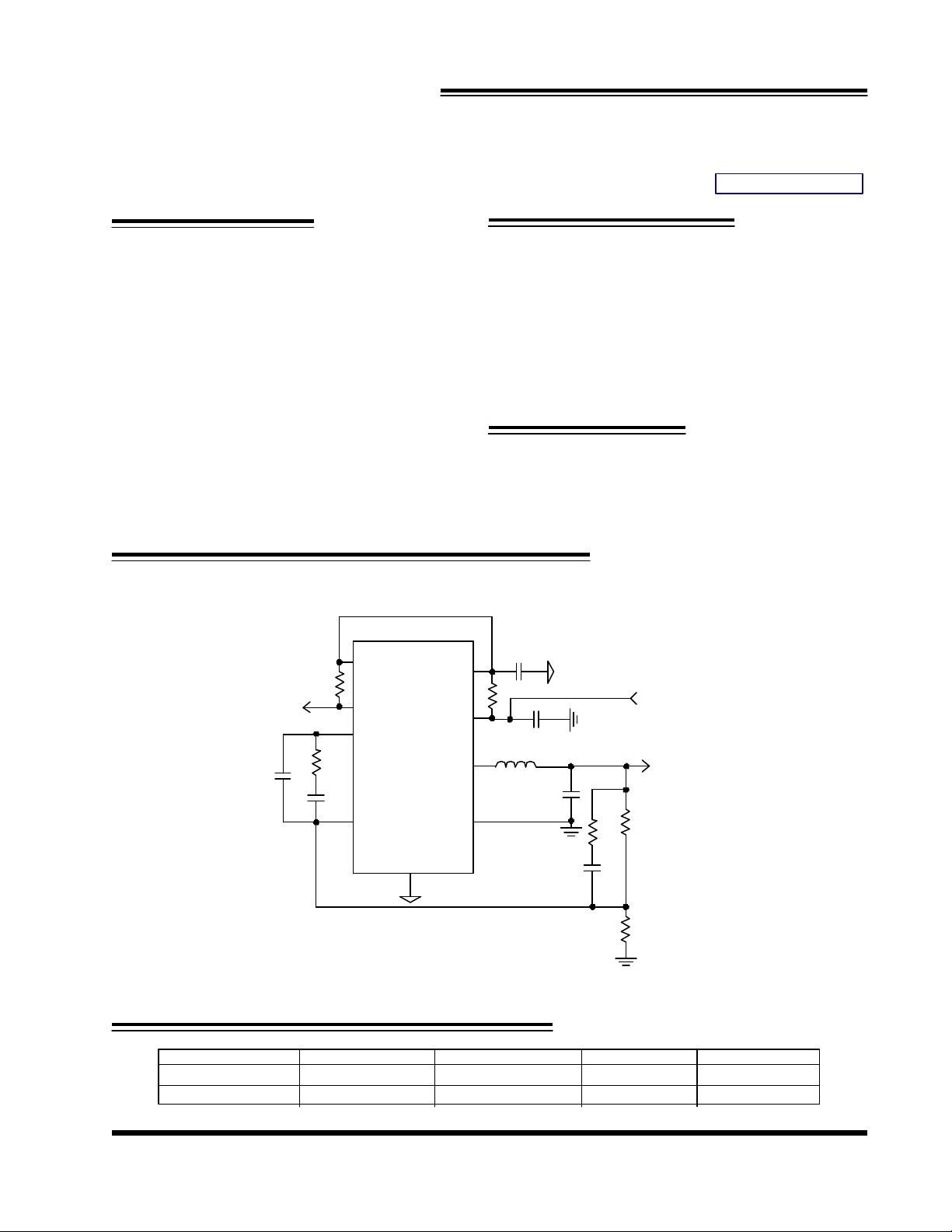
EN
10k
PG
COMP
15k
27p
1.2n
FB
AGND
VDD
VIN
SW
N X 4 1 2 5
PGND
FEATURES
n Feedforward voltage mode control
n 800kHz switching frequency
n <1uA shut-down current
n Peak current limit with hiccup feature and over
temperature protection
n Internal Digital Soft Start
n Over voltage protection
n Available in MLPD-10L and SOICP-8L package
n Power good indicator available
n Pb-free and RoHS compliant
APPLICATIONS
n Li-Ion battery operated portable system
n Low voltage point of load application
n PDA and pocket PC computers
n Portable applications
n Broadband communication and networking
TYPICAL APPLICATION
1uF
10
10uF
2.2uH
47uF
390
680p
2.7V to 4.2V
1.8V
20.5k
16.4k
Figure1 - Typical application of NX4125
ORDERING INFORMATION
Device Temperature Output Voltage Package Pb-Free
NX4125CMTR -10 to 100oC adjustable MLPD-10L Yes
NX4125CSTR -10 to 100oC adjustable SOICP- 8L Yes
Rev. 1.3
05/25/07
www.nexsem.com
1
Page 2
NEXSEM
θ≈52/
CW
C/W
REF
S
NX4125
ABSOLUTE MAXIMUM RATINGS
VIN,EN,FB to GND ...................................... -0.3V to 5.5V
SW to GND ................................................. -1V to 5.5V
ESD Susceptibility .......................................... 1kV
Storage Temperature Range ............................. -55oC to 150oC
Operating Junction Temperature Range ............. -40oC to 125oC
VIN slew Rate ............................................... 3V/uS
CAUTION: Stresses above those listed in "ABSOLUTE MAXIMUM RATINGS", may cause permanent damage to
the device. This is a stress only rating and operation of the device at these or any other conditions above those
indicated in the operational sections of this specification is not implied.
PACKAGE INFORMATION
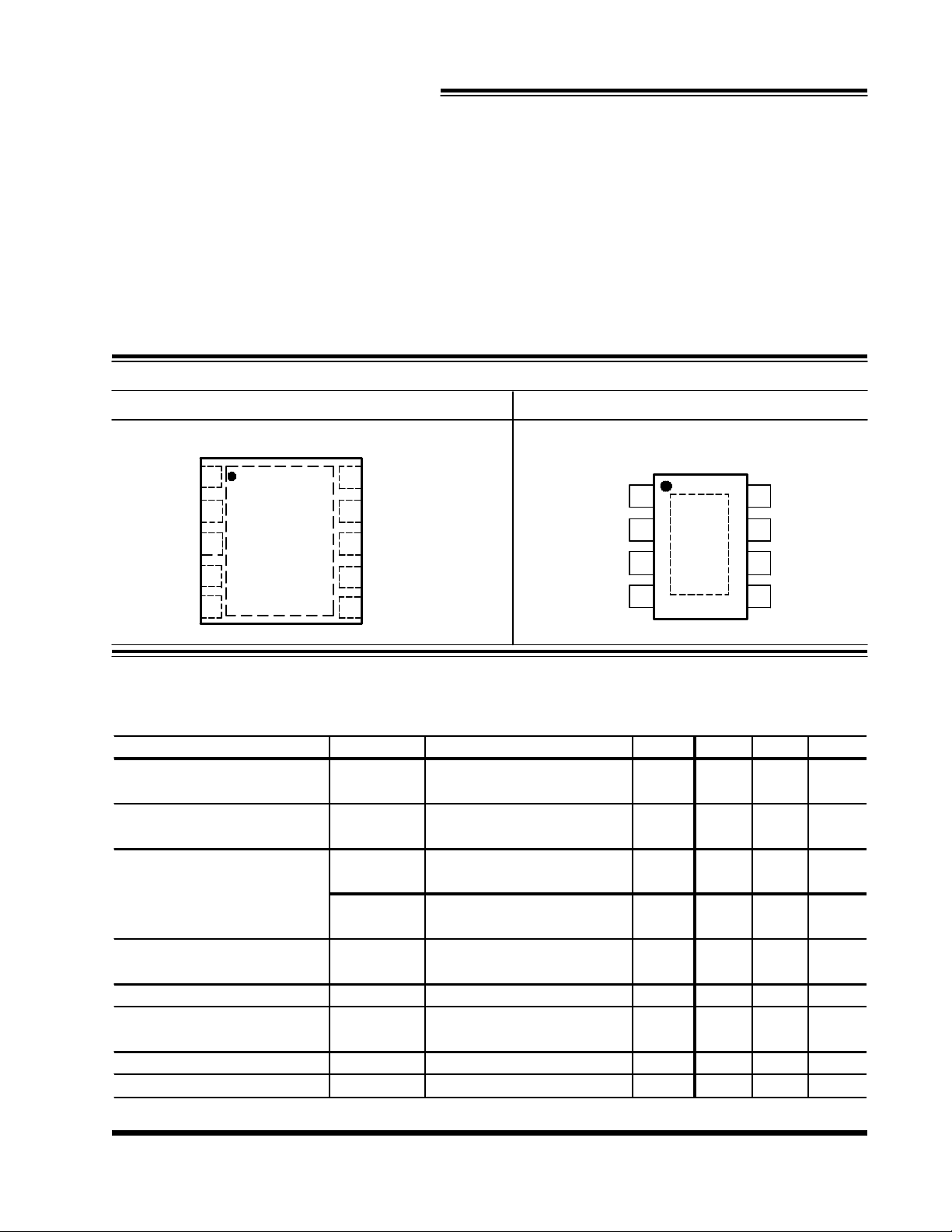
10-LEAD PLASTIC MLPD 8-LEAD PLASTIC SOICP(EXPOSED PAD)
PGND
SW
VIN
VDD
o
JA
1AGND
2
3
4
5
NC
(PAD)
10
9
8
7
6
COMP
FB
NC
PG
EN
AGND
SW
VIN
VDD
θ≈55
1
2
3
4
JA
o
PGND
(PAD)
8
7
6
5
COMP
FB
PG
EN
ELECTRICAL SPECIFICATIONS
Unless otherwise specified, these specifications apply over VIN=VDD=VEN=3.3V, and TA =-10oC to 100oC. Typical
values refer to TA = 25oC. Unless otherwise specified.
PARAMETER SYM Test Condition Min TYP MAX Units
Reference Voltage
Ref Voltage V
Supply Voltage
VIN,VDD Input Voltage V
Supply Current
(shutdown)
IDD (pwm) EN=VDD=VIN 7 mA
CC 2.5
I
DD
EN=GND,VIN=VDD=5V 1 uA
0.8
5.5
V
V
VIN UVLO
VIN start threshold voltage 2.4 V
Hysteresis 0.2 V
Oscillator (Rt)
Frequency F
Max Duty Cycle
Min ON time 70
Rev. 1.3
05/25/07
www.nexsem.com
100
800
kHz
%
nS
2
Page 3
NEXSEM
C
C
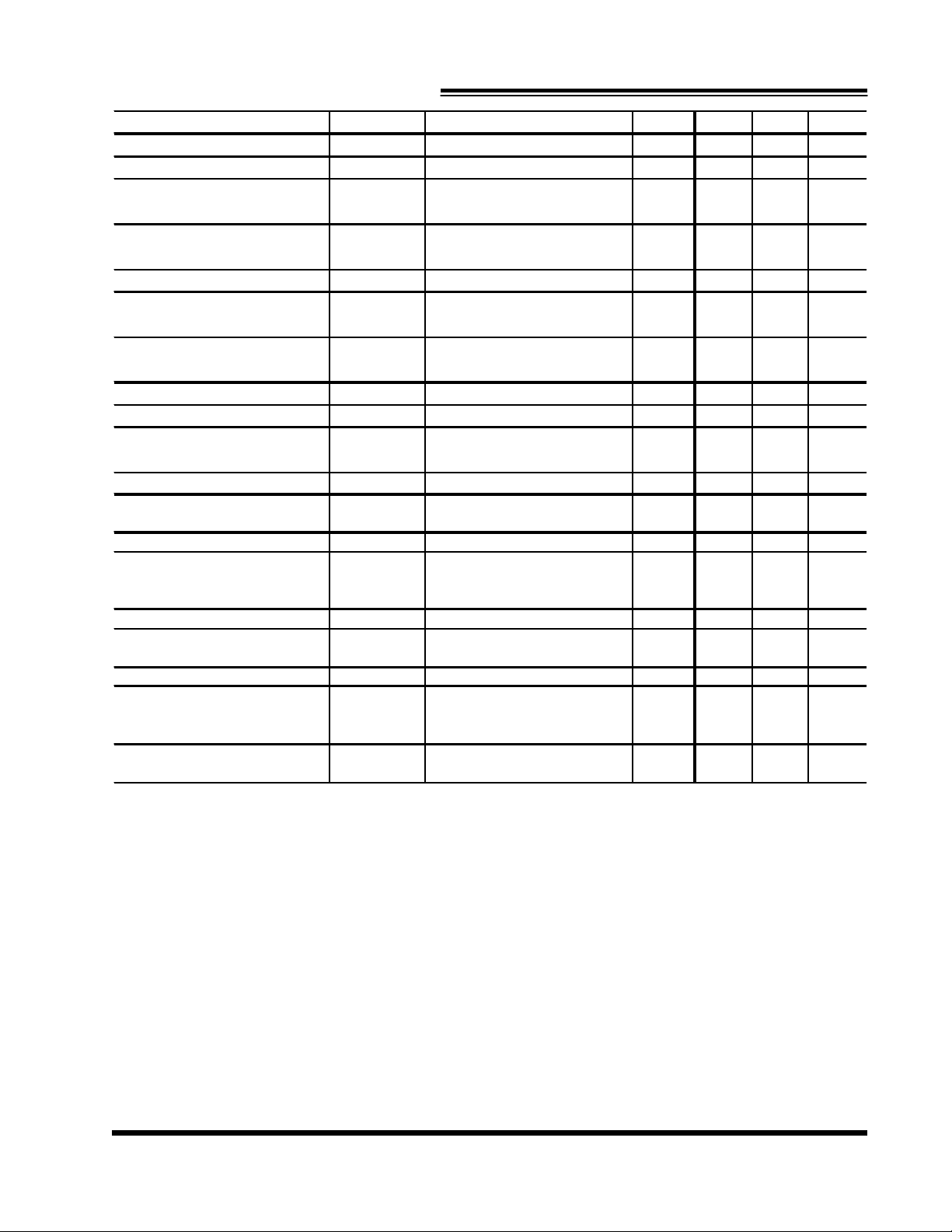
Internal Switch
Rdson of Control FET
VDD=5V
70
mohm
Rdson of Synchronous FET
70
mohm
Power Good(Pgood)
Vref
Hysteresis
5%Over Voltage
Over Voltage Trip Point
130 %Vref
Hysteresis
45
%Vref
Output Voltage
VOUT=1.8V
IOUT=0 to 2A
NX4125
PARAMETER SYM Test Condition Min TYP MAX Units
Ramp-Amplitude Voltage V
Ramp/Vin Gain 0.2 V/V
Error Amplifiers
Feedback Input Bias Current 50 uA
Enable
En low Threshold voltage 0.4 V
En high Threshold voltage 1.4 V
SS
Soft Start time Tss 0.853 mS
Current Limit
Current Limit Threshold 3.5 A
Current limit leading edge
Current Limit response time 200 nS
Thermal Shutdown
Thermal shutdown trip point Note1 165
Hysteresis Note1 20
RAMP
Note1 70 nS
Vin=5V 1 V
o
o
Threshold Voltage as % of
Line Regulation VIN=2.5V to 5.5V IOUT=0A
Load Regulation VIN=3.3V, VOUT=1.8V,
Note. 1. Guaranteed by design and bench test verification, not tested in the final test.
FB ramping up 90 %
0.1
0.5 %
%V
Rev. 1.3
05/25/07
www.nexsem.com
3
Page 4
NEXSEM
PIN DESCRIPTIONS
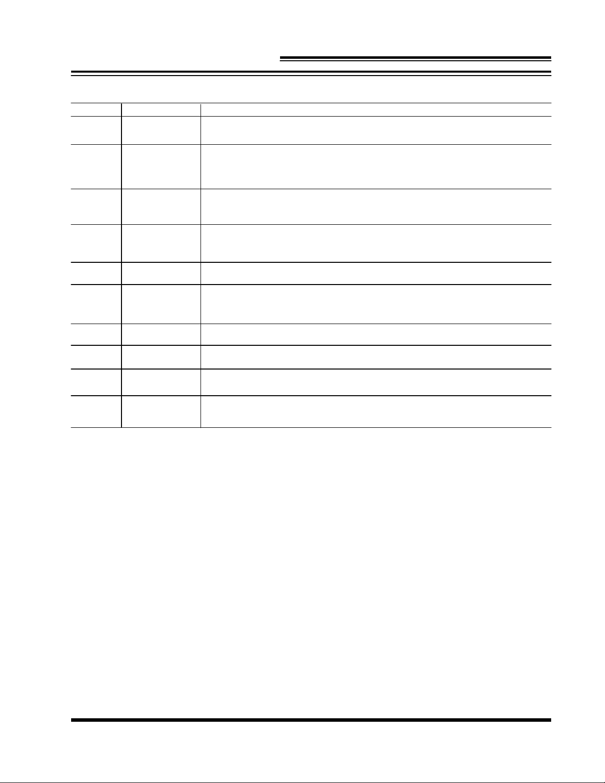
PIN # PIN SYMBOL PIN DESCRIPTION
NX4125
1
2
3
4
5
6
7
8
9
10
AGND
PGND
SW
VIN
VDD
EN
PG
NC
FB
COMP
Control circuitry ground.
Ground Connection for Chip. Connect PGND with large copper areas to the
input and output supply returns, and negative terminals of the input and output
capacitors.
SW output. Junction of the internal high-side, low-side power MOSFETs and
output inductor.
Power pin for the power stage. A 10uF ceramic cap is suggested to decoupled
from this pin to power ground.
Power pin for the control circuitry.
Enable Input. Set this pin to gnd or less than 0.4V will shut down the regulator.
Set this pin above 1.4V, the regulator will be in operation.
Power good goes high when the FB pin voltage above 90% Vref.
Not used pin.
Error amplifier inverting input. Connect to an external resistor divider.
This pin is the output of the error amplifier and together with FB pin is used to
compensate the voltage control feedback loop.
Rev. 1.3
05/25/07
www.nexsem.com
4
Page 5
NEXSEM
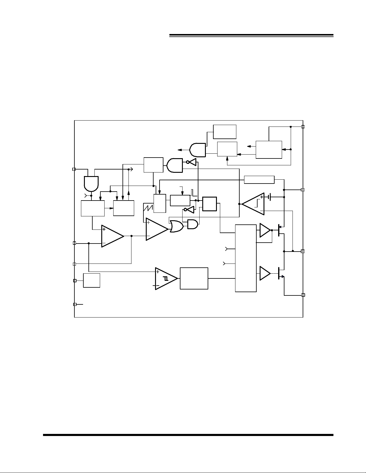
BLOCK DIAGRAM
NX4125
EN
FB
COMP
PG
AGND
start
Soft start
Vref
Power
Goood
CLK
Hiccup
timer
16 cycle
counter
OCPB
Vref*130%/85%
OSC
POR
LED
70ns
one shot
3 cycle filter
Thermal
Shutdown
reset dom
S
Q
R
OCPB
Start
UVLO
PWM
OVP
Vref
Feed Forward
Control
Logic
VDD
Bias
Generator
VIN
+
SW
PGND
Rev. 1.3
05/25/07
Figure 2 - Simplified block diagram of the NX4125
www.nexsem.com
5
Page 6
NEXSEM
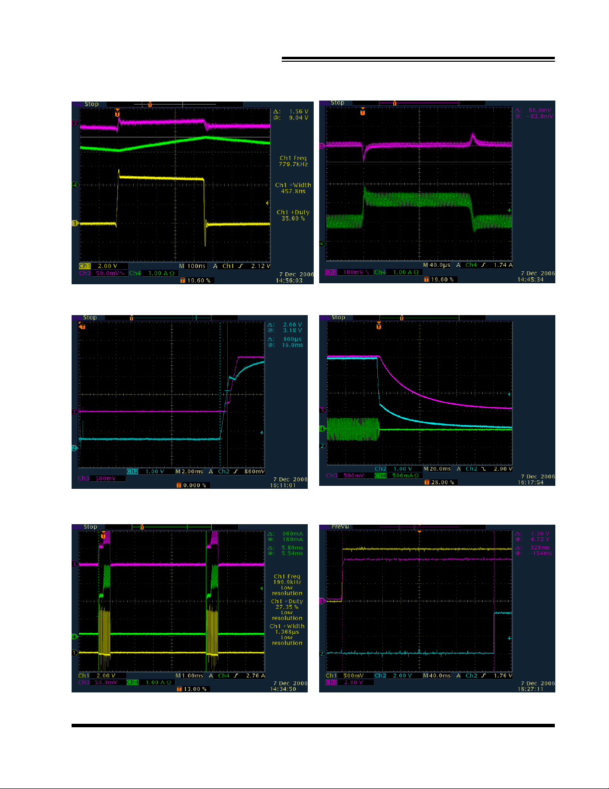
Demo board Waveform
NX4125
Figure 3: Sw and ripple (VIN=5V, VOUT=1.5V)
Figure 5: Startup
Figure 4: Dynamic response (VIN=5V, VOUT=3.3V)
Figure 6: Turnoff
Figure 7: Short protection Figure 8: Pgood delay(Ch2 pgood)
Rev. 1.3
05/25/07
www.nexsem.com
6
Page 7
NEXSEM
Eff (%)
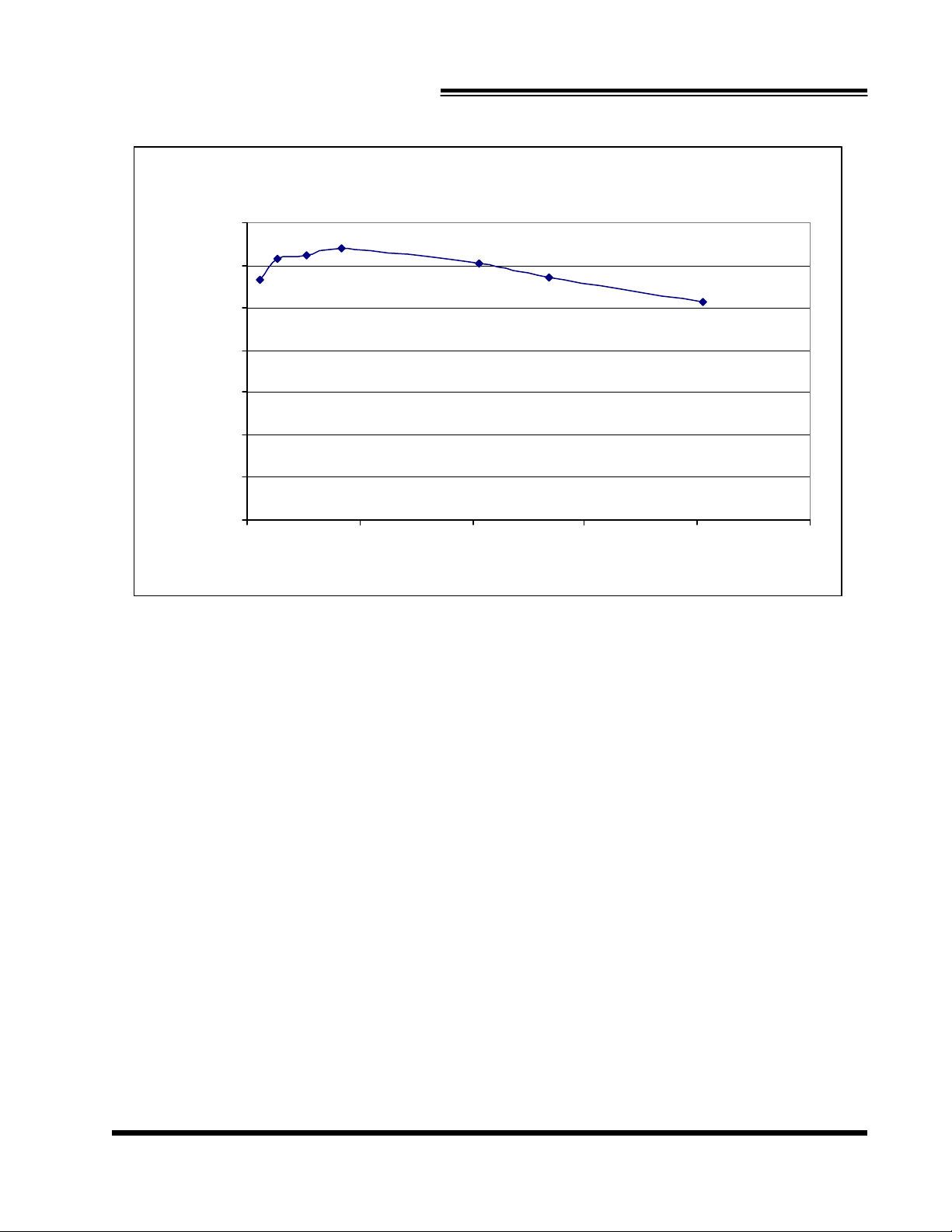
NX4125 Eff Test, Vin=2.7V, Vout=1.5V
100.00%
90.00%
80.00%
70.00%
60.00%
50.00%
40.00%
30.00%
0.000 0.500 1.000 1.500 2.000 2.500
NX4125
Figure 9: Efficiency
Iout (A)
Rev. 1.3
05/25/07
www.nexsem.com
7
 Loading...