

Page 1
NX4110
1A SYNCHRONOUS BUCK SWITCHER WITH FET ON BOARD
ADVANCE DATA SHEET
Pb Free Product
DESCRIPTION
The NX4110 is a current mode PWM buck switcher with
internal compensation, can provides up to 1A output
current with FET on board. It operates from 2.7V to 5.5V
and output as low as 0.6V which is ideal for the application with single cell Li-Ion battery as well as other 3.3V
input bus supply applications. Switching frequency is
fixed 1MHz, small surface mount inductors and capacitors are allowed to use, make it good for portable applications.
NX4110 is available in 5-pin SOT23 package.
5
FB
VIN
NX4110
FEATURES
n SOT23-5L package
n Internal Digital Soft Start
n Internally-compensated Current mode controller
n Peak Current Limit with HICCUP feature and Over
temperature protection
n Prebias start up Operation
n Pgood available
n Fixed 1.2V, 1.5V, 1.8V versions and adjustable
version are available
n 100% duty ratio operation capability
n Pb-free and RoHS compliant
APPLICATIONS
n Li-Ion battery operated portable system
n Cellular Phones
n Portable applications
n USB Devices
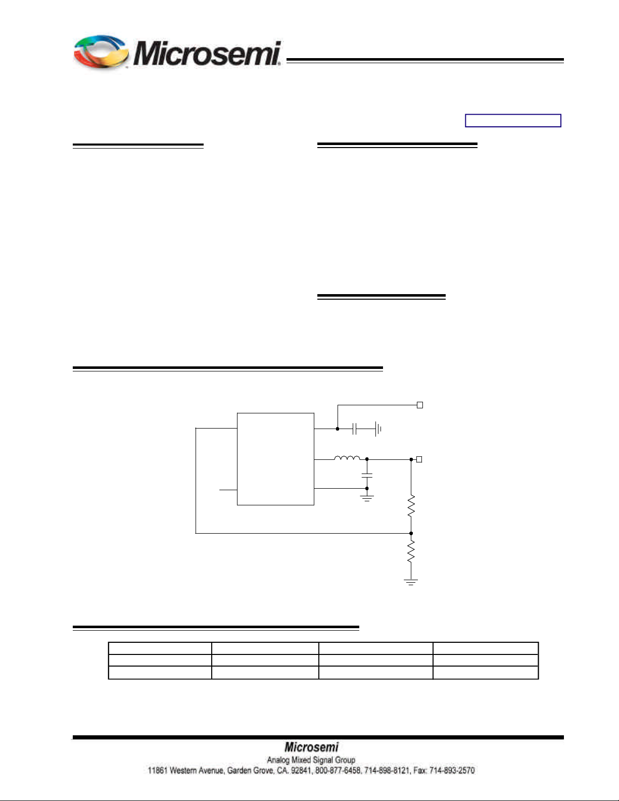
TYPICAL APPLICATION
VIN=5V
22uF(X5R,6.3V)
4
1
PGOOD
Fig.1 - Typical application of NX4110CZ1TR
Device Temperature Package Pb-Free
NX4110CZ1TR -40oC to 85oC SOT23-5L Yes
NX4110-XXCZ1TR -40oC to 85oC SOT23-5L Yes
Note: Fixed output voltage identification.
XX=12 Fixed Output Voltage=1.2V XX=15 Fixed Output Voltage=1.5V
XX=18 Fixed Output Voltage=1.8V
SW
GND
2.2uH
3
2
10uF
(X5R, 6.3V)
Vout=2.5V
332k
105k
ORDERING INFORMATION
Rev. 1.7
06/04/09
1
Page 2
NX4110
CW
θ≈110/
IOUT=10mA
ABSOLUTE MAXIMUM RATINGS
VIN,VDD to GND .............................................................. -0.3V to 6V
SW,FB,EN to GND ........................................................... -0.3V to VIN + 0.3V
ESD Susceptibility ............................................................. 1kV
Lead Temperature(Soldering,10sec.) .................................... 300oC
Storage Temperature Range ................................................ -55oC to 150oC
Operating Junction Temperature Range ................................ -40oC to 150oC
CAUTION: Stresses above those listed in "ABSOLUTE MAXIMUM RATINGS", may cause permanent damage to
the device. This is a stress only rating and operation of the device at these or any other conditions above those
indicated in the operational sections of this specification is not implied.
PACKAGE INFORMATION
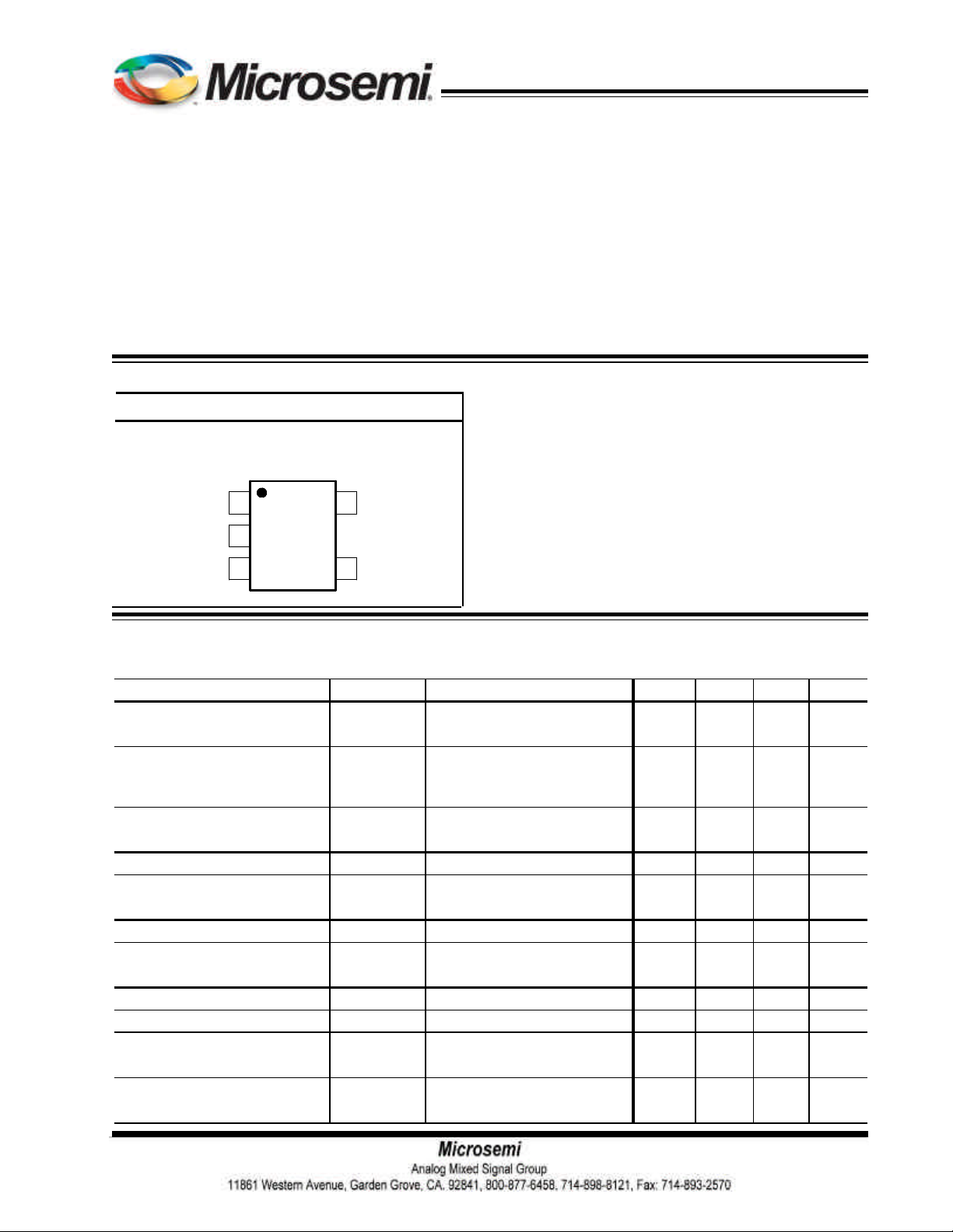
5-LEAD PLASTIC SOT23
o
FB
5
VIN
4
PGOOD
GND
SW
JA
1
2
3
ELECTRICAL SPECIFICATIONS
VIN=5V. Typical data refers to TA= 25oC. Unless otherwise specified.
PARAMETER SYM Test Condition Min TYP MAX Units
Reference Voltage
Ref Voltage V
Line Regualtion
Line Regulation VIN=3V to 5V,VOUT=1.8V,
VIN UVLO
VIN rising threshold 2.5 V
VIN falling threshold 2.4 V
Supply Voltage(VIN)
VIN Input Voltage Range V
Quiescent Current
Oscillator (Rt)
Frequency F
Max Duty Cycle 70
Min ON time 100
Error Amplifiers
Feedback Input Bias Current 0.05 uA
SS
Soft Start time Tss 420 uS
REF
IN
I
q
S
No Load, adjustable output 25 50 uA
2.7
0.6
2
1
5.5
MHz
V
mV
V
%
nS
Rev. 1.7
06/04/09
2
Page 3
NX4110
PARAMETER SYM Test Condition Min TYP MAX Units
Current Limit
Current Limit Threshold 1.8 A
Thermal Shutdown
Thermal shutdown trip point 155
Hysteresis 15
Internal Switch
Rdson of Control FET
Rdson of Synchronous FET
PGOOD
PGOOD low Threshold
PGOOD high Threshold
voltage
90 %V
Vin=5V 400
Vin=3.3V 480
Vin=5V 300
Vin=3.3V 360
PIN DESCRIPTIONS
PIN SYMBOL PIN DESCRIPTION
SW
SW output. Junction of the internal high-side and low-side power MOSFETs, and
output inductor.
85 %V
mohm
mohm
o
C
o
C
REF
REF
GND
FB
VIN
PGOOD
Ground Connection for Chip. Connect GND with large copper areas to the input and
output supply returns, and negative terminals of the input and output capacitors.
Error amplifier inverting input. Connect directly to output voltage for fixed version of
chip. Connect to an external resistor divider for the adjustable version. A 332kohm
resistor is recommended to be connected from VOUT and FB for adjustable version.
Supply voltage input for switcher. This pin needs minimum 22uF/X5R/6.3V as input
capacitor.
PGOOD indicator. It requires a pull up resistor to Vcc or lower voltage. When FB pin
reaches 90% of the reference voltage PGOOD transitions from LO to HI state.
Rev. 1.7
06/04/09
3
Page 4
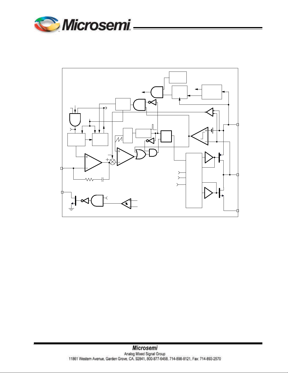
BLOCK DIAGRAM
NX4110
Thermal
Shutdown
FB
PGOOD
VIN
start
POR
Soft start
Vref
CLK
1Mohm
Hiccup
timer
20pF
3 cycle
counter
OCPB
PWM comparator
SS_finished
OSC
POR
70ns
one shot
FB
0.9*Vref
reset dom
S
Q
R
OCPB
POR
VIN
UVLO
PWM
LDen
Vref
Control
Logic
Bias
Generator
+
-
+
VIN
SW
GND
Rev. 1.7
06/04/09
Fig. 2 - Simplified block diagram of the NX4110
4
Page 5
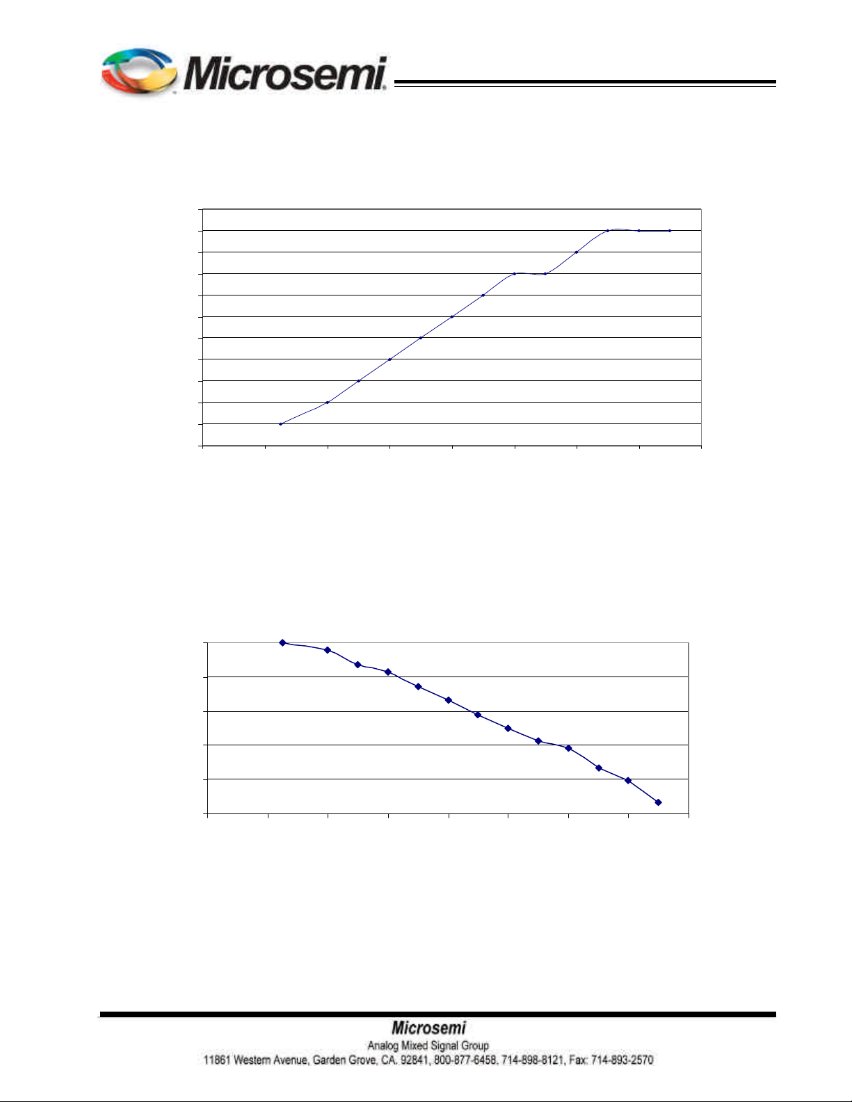
Typical Operating Characteristics
Normalized Frequency
Reference voltage vs temperature
0.604
0.603
0.602
0.601
0.6
0.599
0.598
0.597
Reference voltage(V)
0.596
0.595
0.594
0.593
0 20 40 60 80 100 120 140 160
NX4110
temperature(°C)
Fig.3 - Reference volateg vs temperature
Normalized frequency vs temperature
1
0.98
0.96
0.94
0.92
0.9
0 20 40 60 80 100 120 140 160
temperature(°C)
Fig.4 - Normalized frequency vs temperature
Rev. 1.7
06/04/09
5
Page 6
1200
Output Current (mA)
1000
800
600
400
200
NX4110
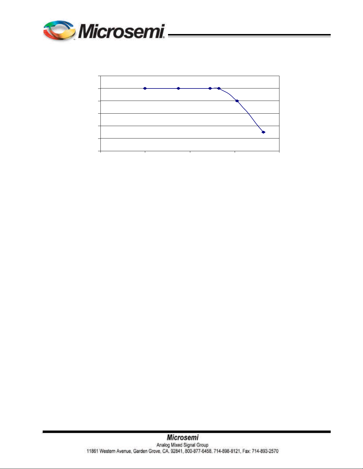
Duty Cycle vs Maximum Output Current
0
0 20 40 60 80
Duty cycle (%)
Fig.5 - Duty cycle vs maximum output current
Rev. 1.7
06/04/09
6
Page 7
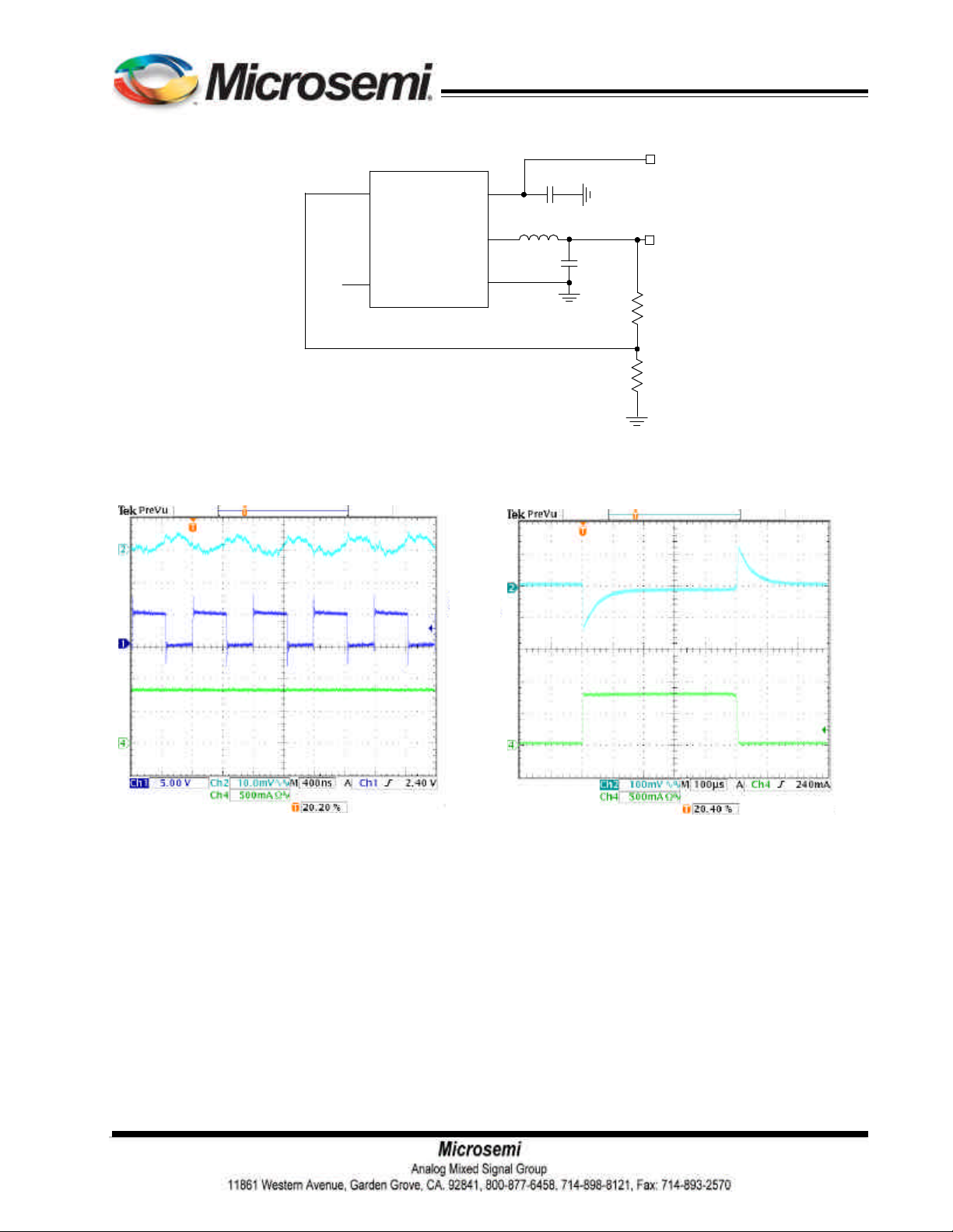
Typical Application( VOUT=2.5V)
5
FB
1
PGOOD
Fig. 6 - Demo board schematic
VIN
NX4110
SW
GND
4
2.2uH
3
2
22uF(X5R,6.3V)
10uF
(X5R, 6.3V)
NX4110
VIN=5V
Vout=2.5V
332k
105k
Fig. 7 - Output ripple
Rev. 1.7
06/04/09
Fig. 8 - Transient response
7
Page 8
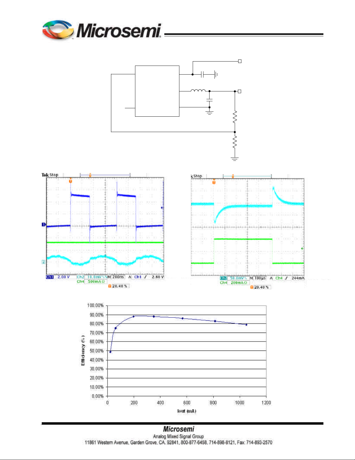
Typical Application( VOUT=1.8V)
5
FB
1
PGOOD
Fig. 9 - Demo board schematic
VIN
NX4110
SW
GND
4
2.2uH
3
2
22uF(X5R,6.3V)
10uF
(X5R, 6.3V)
NX4110
VIN=5V
Vout=1.8V
332k
165k
Fig. 10 - Output ripple
Rev. 1.7
06/04/09
Fig. 11 - Transient response
Fig. 12 - Efficiency
8
Page 9
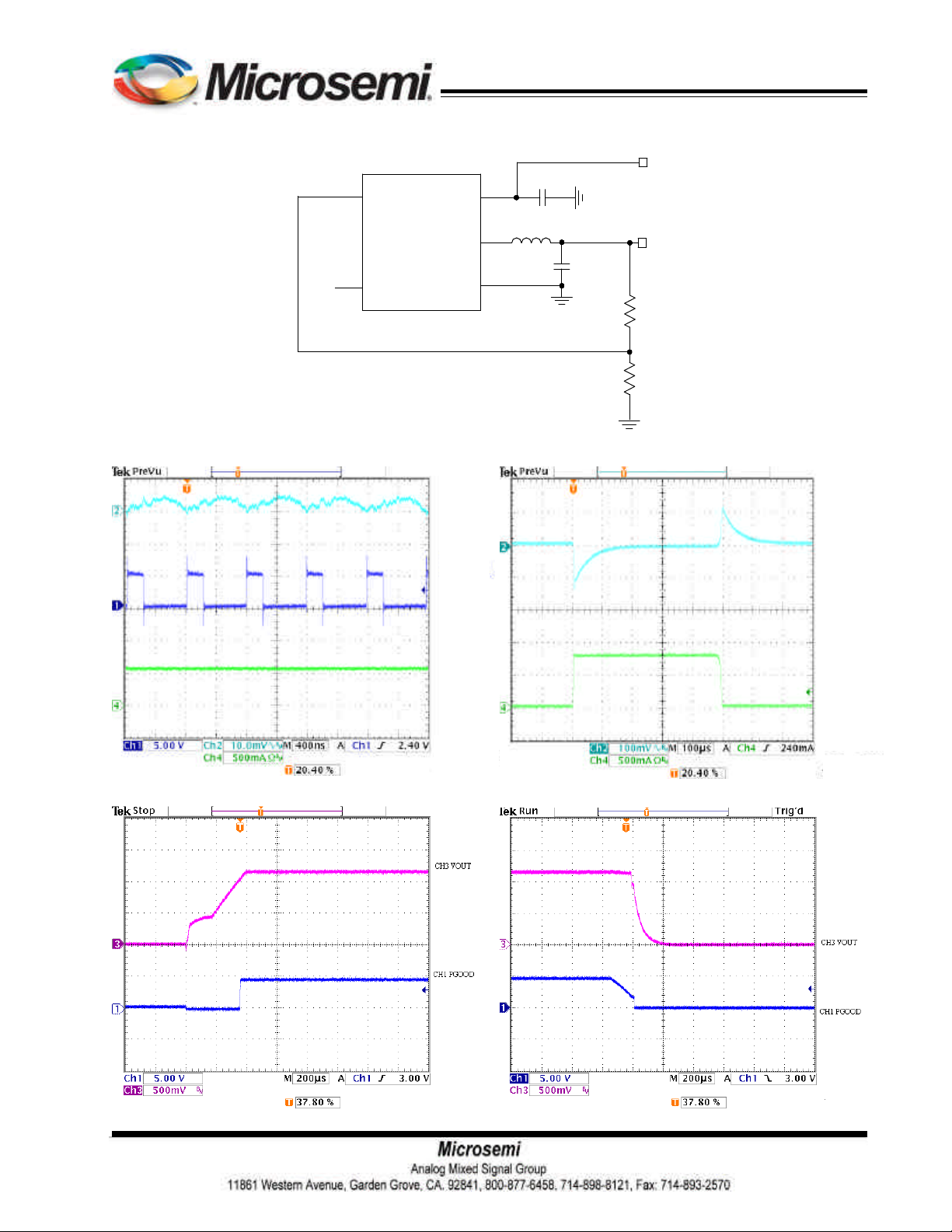
Typical Application( VOUT=1.2V)
5
FB
1
PGOOD
Fig. 13 - Demo board schematic
VIN
NX4110
SW
GND
4
2.2uH
3
2
22uF(X5R,6.3V)
10uF
(X5R, 6.3V)
NX4110
VIN=5V
Vout=1.2V
332k
332k
Fig. 14 - Output ripple
Fig. 16 - Startup
Rev. 1.7
06/04/09
Fig. 15 - Transient response
Fig. 17 - Shutdown
9
Page 10
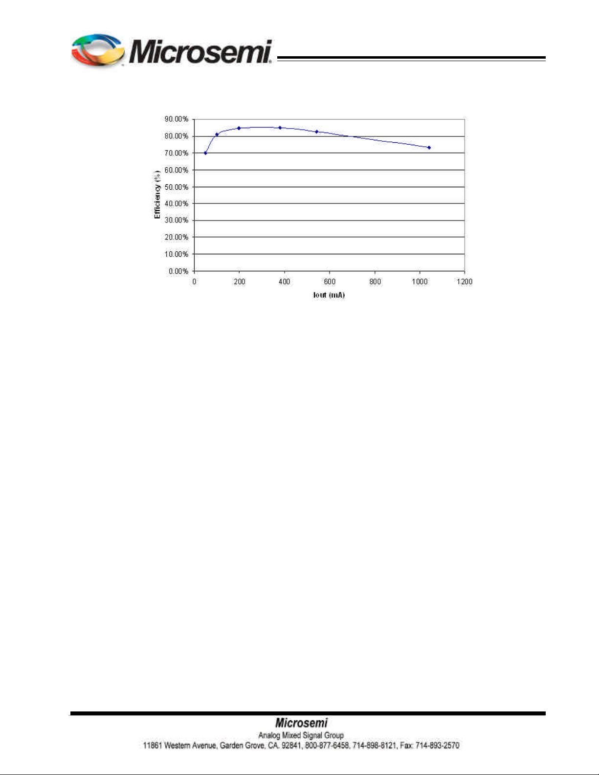
Typical Application( VOUT=1.2V)
NX4110
Fig. 18 - Efficiency
Rev. 1.7
06/04/09
10
Page 11
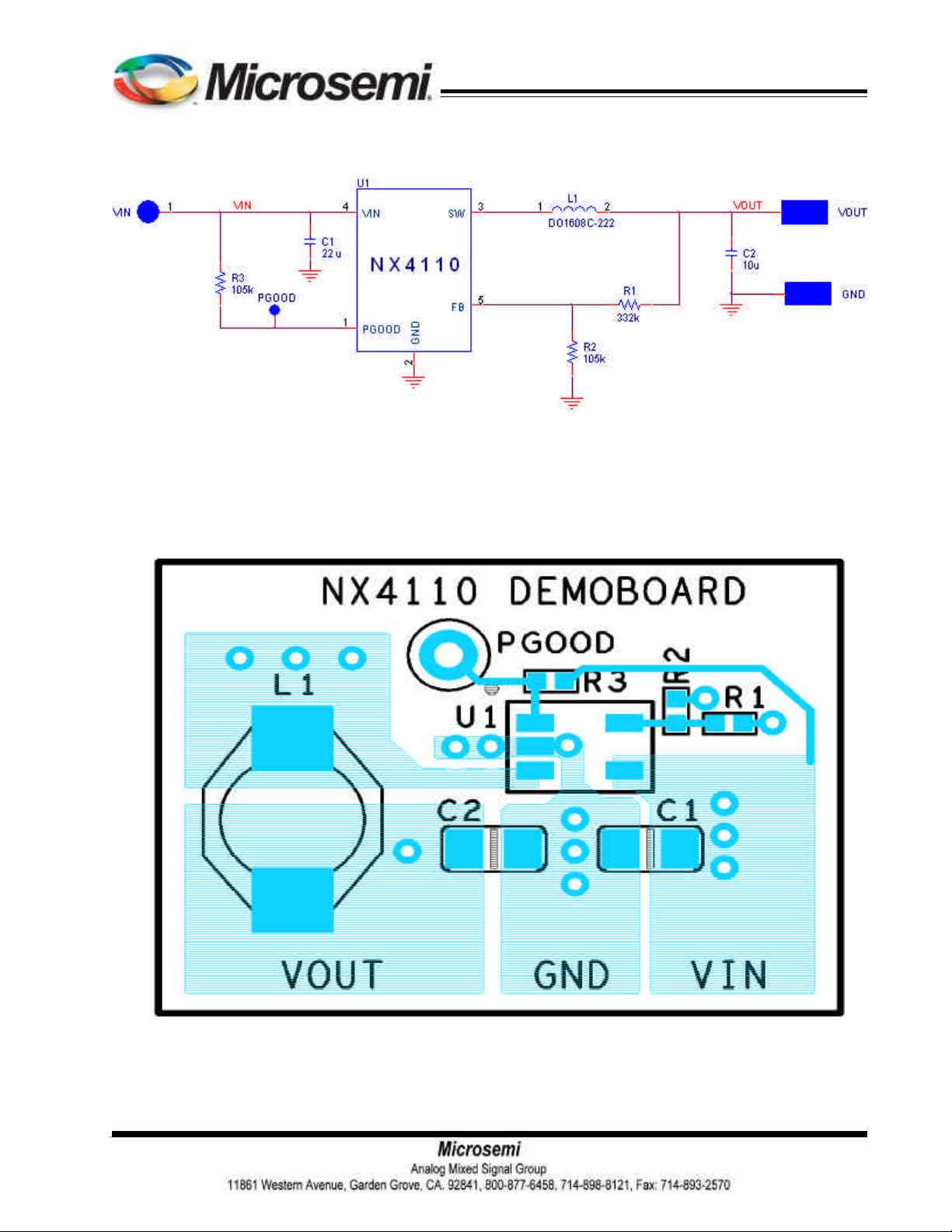
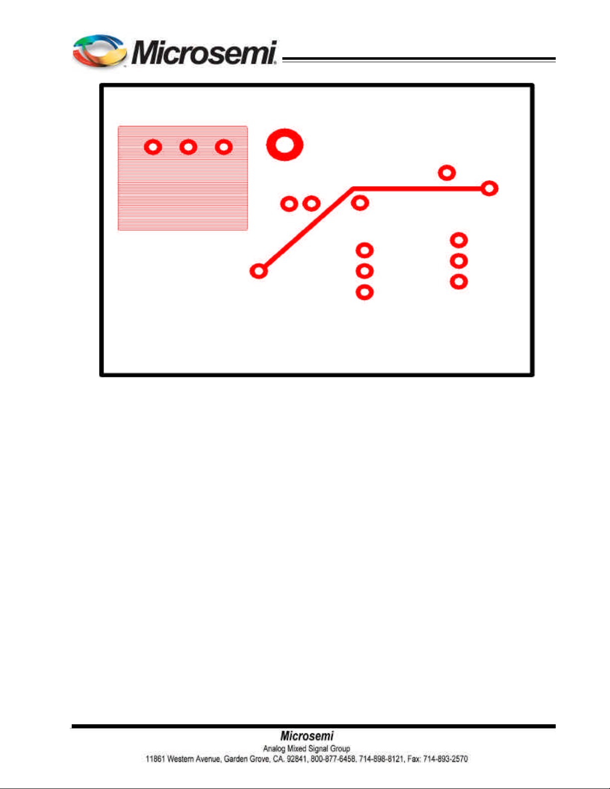
Demoboard Layout
NX4110
Fig. 19 - Demoboard schematic
Rev. 1.7
06/04/09
Fig. 20- Top layer
11
Page 12
NX4110
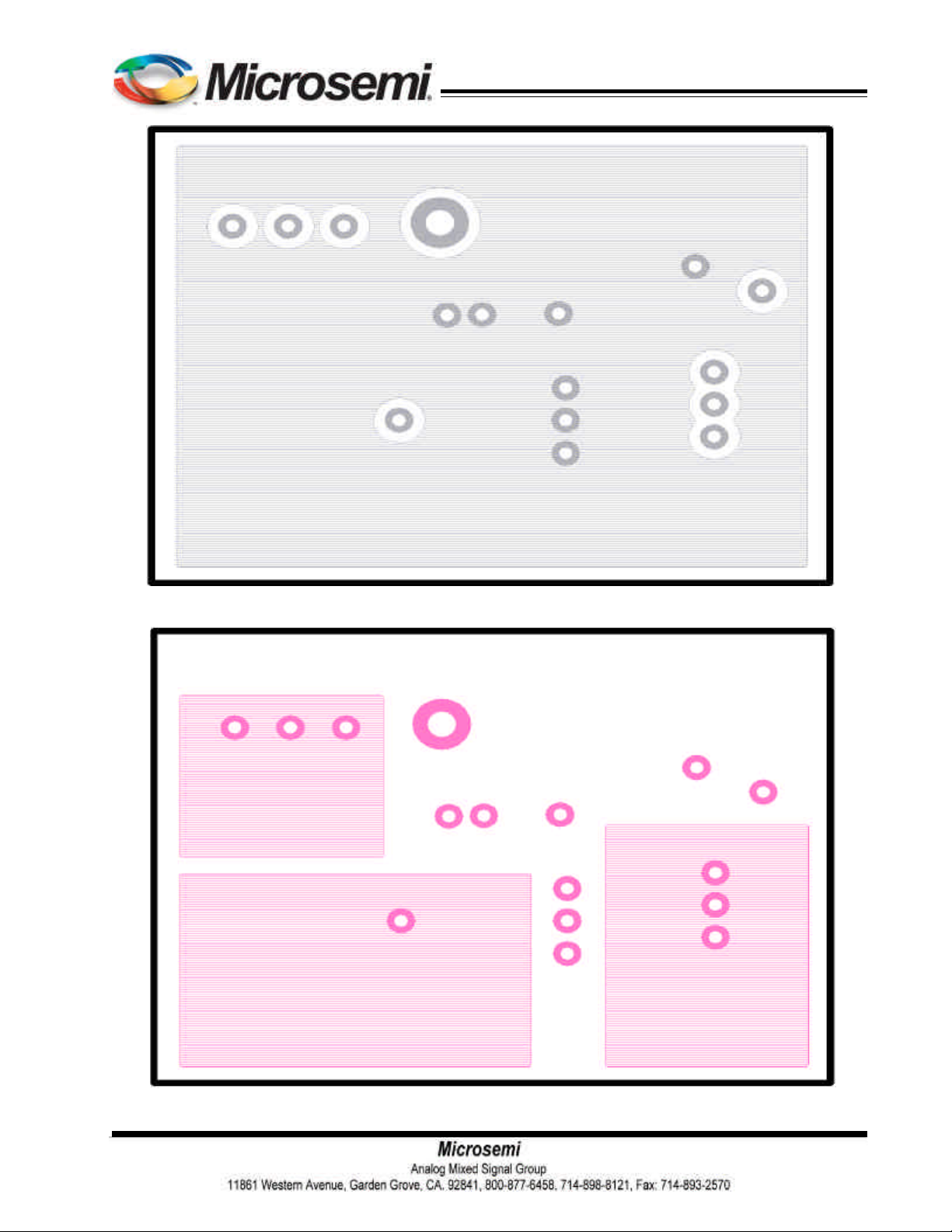
Fig. 21 - Gound layer
Rev. 1.7
06/04/09
Fig. 22 - Power layer
12
Page 13
NX4110
Fig. 23 - Bottom layer
Rev. 1.7
06/04/09
13
Page 14
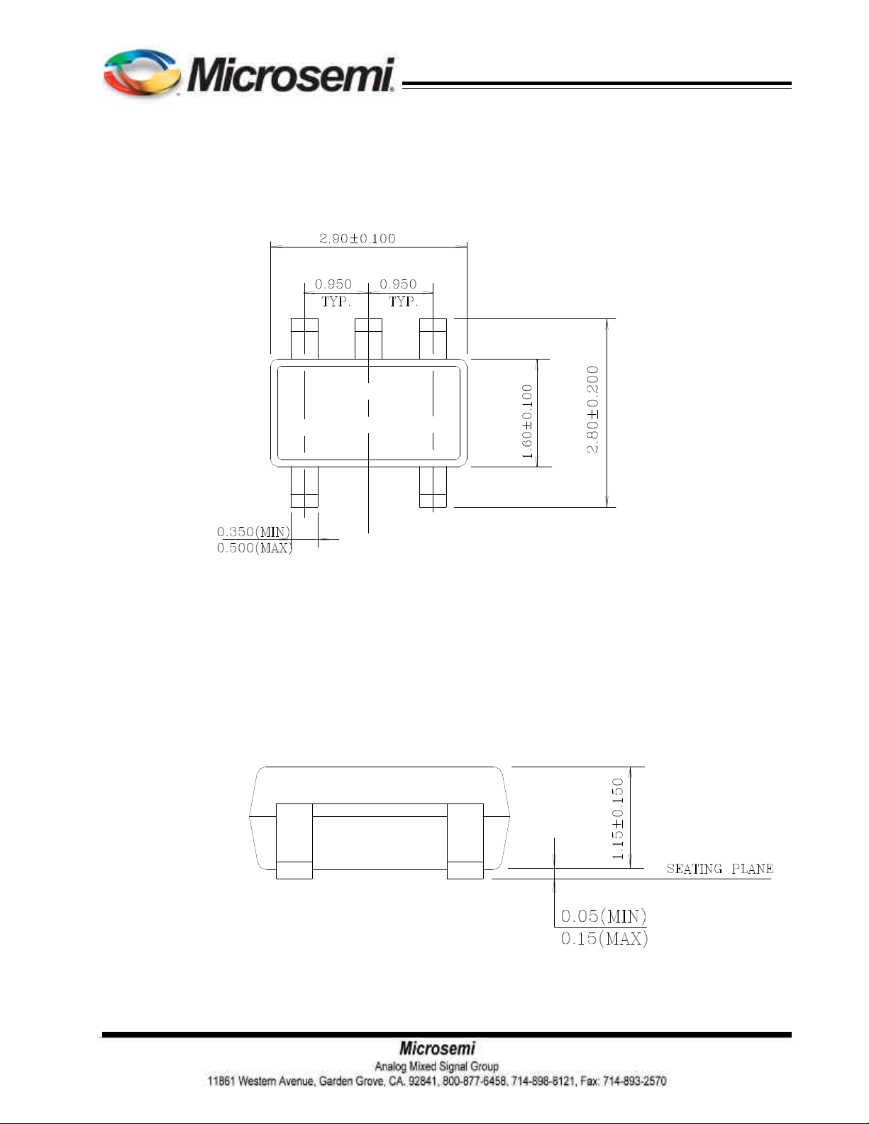
SOT23 5 PIN PACKAGE OUTLINE DIMENSIONS
NX4110
Top View
Side View
Rev. 1.7
06/04/09
14
 Loading...