

Page 1
Evaluation board available.
NEXSEMNEXSEM
NEXSEM
NEXSEMNEXSEM
DUAL SYNCHRONOUS PWM CONTROLLER WITH NMOS LDO
CONTROLLER & 5V BIAS REGULA TOR
DESCRIPTION
The NX2601 controller IC is a triple controller with a dual
channel synchronous Buck controller IC and an LDO
controller designed for multiple converters such as PCIe
graphic card applications .The two synchronous PWM
controllers are 180 degree out of phase which reduces
the input ripple current, allowing to reduce the # of input
capacitors.Another main feature of the part is that it can
operate from single 12V supply while maintaining a regulated 5V supply for the biasing and the internal drivers.
Other features of NX2601 are; programmable frequency
from 200kHz to 1MHz, independent digital soft start and
enable pins for each controller which allows for different
power sequencing, Adaptive driver provides optimized
efficiency while maintain sufficient deadband, Vcc
undervoltage lock out and current limiting using an Rdson of the external MOSFET with HICCUP feature.
NX2601
PRELIMINARY DA T A SHEET
FEATURES
Two channel PWM with out of phase operation
Individual digital soft start for two PWM output and
LDO controller
Bus voltage operation from 2V to 25V
Hiccup Current limit by sensing Rdson of MOSFET
Adjustable frequency up to 1Mhz per channel
Adaptive deadband time
Three enable pin available allows for independent
power sequencing
MLPQ-32L package offers small size
APPLICATIONS
PCIe Graphic Card on board converters
Vddq Supply in mother board applications
On board DC to DC such as
12V to 3.3V, 2.5V or 1.8V
FPGA and Set Top Box Applications
+5V
VIN1
VIN2
+3.3V
VOUT3
+2.5V/2A
OFF
ON
R25
C20
150uF
10k
2N3904
R26
10k
VIN1
OFF
R27
ON
10k
P ATENT PENDING
Device Temperature Package Frequency
NX2601CMTR 0 to 70oC MLPQ-32L 200kHz to 1MHz
150uF
10k
R28
2N3904
M5
C19
2N3904
C17
68uF
1.5k
6.8k
6.8k
R18
R20
R22
R16
5k
R24
C21
C24
0
C25
1uF
47pF
C16
R15
62k
1nF
10
R11
11
10
9
8
7
3
1
2
6
30
31
REG FB
REG OUT
AVXVCC
LDO OUT
LDO FB
ENLDO
ENSW1
ENSW2
RT
VP
VREF
C15
1uF
VCC
GND
5
PVCC1
HDRV1
OCP1
LDRV1
PGND1
Comp1
PVCC2
N X 2 6 0 1
HDRV2
OCP2
LDRV2
PGND2
Comp2
4
BST1
SW1
Fb1
BST2
SW2
Fb2
C1
23
1uF
D1
24
C4
0.1uF
25
26
R1
10.5k
27
22
21
29
R5 5k
28
220pF
C22
C8
18
1uF
D2
17
C11
0.1uF
16
15
R6
3k
14
19
20
12
R10
13
5k
220pF
C23
1uF
150pF
R17
2.35k
R21
1.25k
R23
1.25k
R12
5k
R13
1.65k
C18
R19
1.25k
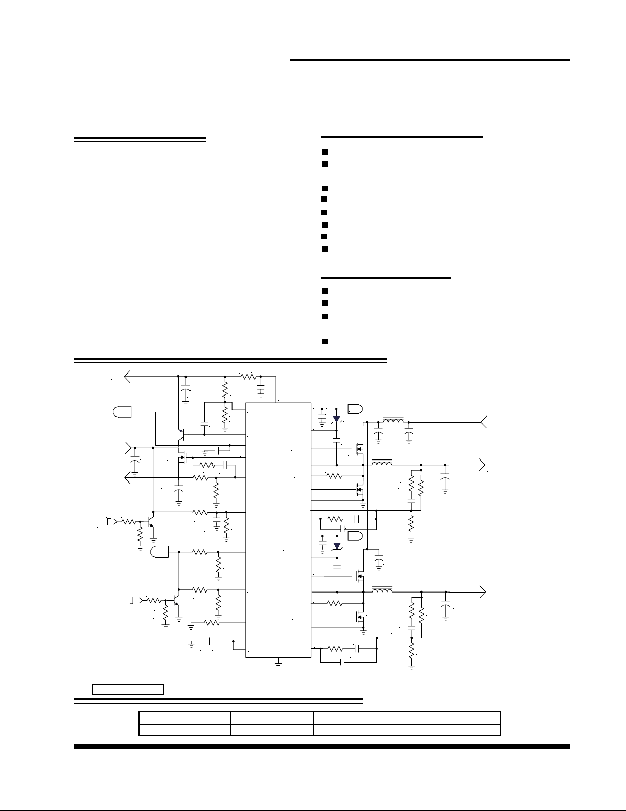
Figure1 - T ypical application of 2601
TYPICAL APPLICA TION
+5V
M1
M2
+5V
10nF
C12
C58.2nF
L2 0.78uH
M3
L4 1.5uH
M4
L1 1uH
C2
180uF
2.7nF
C9
180uF
3.3nF
1.5k
C6
820
C13
VIN1
C3
100uF
C7
R2
R4
20.8k
R7
R9
6.97k
2 x (2R5TPD680M6,680uF,6m ohm )
R3
10.4k
C14
3 x (4TPE150M,150uF,18mohm )
R8
8.7k
+12V
VOUT1
+1.2V@15A
VOUT2
+1.8V/10A
ORDERING INFORMA TION
Rev. 1.0
01/24/05
www.nexsem.com
1
 Loading...