

Page 1
NEXSEM
NX2420
TWO PHASE SYNCHRONOUS PWM CONTROLLER WITH
INTEGRATED FET DRIVER AND DIFFERENTIAL CURRENT SENSE
PRELIMINARY DATA SHEET
Pb Free Product
DESCRIPTION
The NX2420 is a two-phase PWM controller with integrated FET driver designed for low voltage high current
application. The two phase synchronous buck converter
offers ripple cancelation for both input and output. The
NX2420 uses differential remote sensing using either current sense resistor or inductor DCR sensing to achieve
accurate current matching between the two channels.
Differential sensing eliminates the error caused by PCB
board trace resistance that is otherwise is present when
using a single ended voltage sensing. In addition the
NX2420 offers high drive current capability especially for
keeping the synchronous MOSFET off during SW node
transition, accurate programmable droop allowing to reduce number of output capacitors, accurate enable circuit provides programmable start up point for Bus voltage, PGOOD output, programmable switching frequency
and hiccup current limiting circuitry.
C30
R36
R32
ON
R46
R37
OFF
R33
R34
VOUT
R47
R48
+5V
C32
R44
C33
R35
C35
R45
C36
C34
R31
2N3904
C37
5
21
22
3
15
4
14
11
10
12
13
ENBUS
DROOP
PVCC
5VCC
REFIN/EN
AGND
CSCOMP
RT
IOUT/IMAX
VCOMP
FB
PGND(PAD)
BST1
HDRV1
SW1
LDRV1
CS+1
CS-1
BST2
N X 2 4 2 0
HDRV2
SW2
LDRV2
CS+2
CS-2
INREFOUT/POK
FEATURES
n Differential inductor DCR sensing eliminates the
problem with layout parasitic
n External programmable voltage droop
n Low Impedance On-board Drivers
n Hiccup current limit and IOUT indication
n Power Good for power sequencing
n Enbus allows programming the BUS voltage
start up threshold
n Programmable frequency
n Prebias start up
n OVP protection without negative spike at output
n Selectable between internal and external reference
n Pb-free and RoHS compliant
APPLICATIONS
n Graphic card High Current Vcore Supply
n High Current on board DC to DC converter
applications
TYPICAL APPLICATION
+5V
2
1
24
23
6
7
17
18
19
20
9
8
16
C42
C43
+5V
R27
C31
C21
C10
C11
C20
Q1
Q2
Q3
Q4
Ref for external circuitry
L1
R43
C41
C25 C24
L2
R42
C40
C22C23
R41
C26C27
R40
VIN
VOUT
Rev.1.9
05/06/08
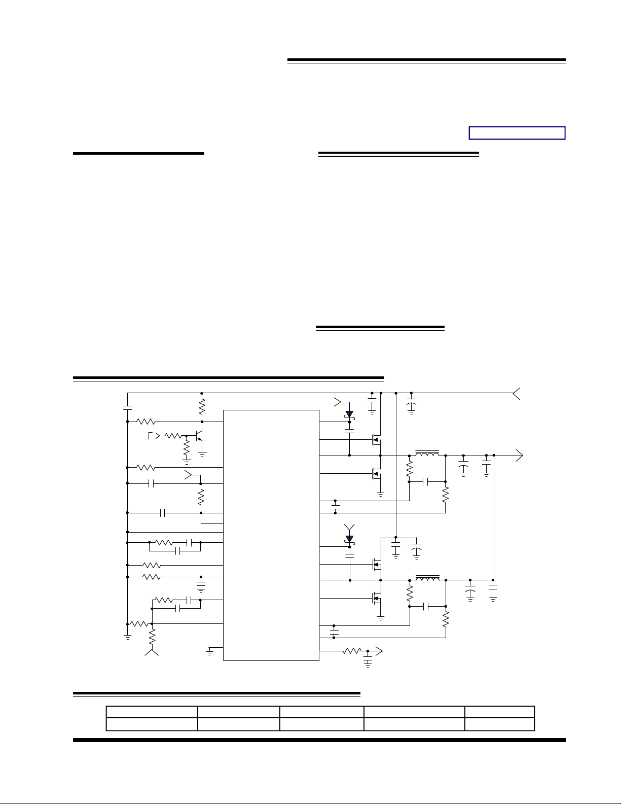
Figure1 - Typical application of NX2420
ORDERING INFORMATION
Device Temperature Package Frequency Pb-Free
NX2420CMTR 0 to 70oC MLPQ 4x4 - 24L 50kHz to 1MHz Yes
www.nexsem.com
1
Page 2
NEXSEM
CW
θ≈30.5/
PARAMETER
SYM
TEST CONDITION
MIN
TYP
MAX
UNITS
Supply Voltage(Vcc)
NX2420
ABSOLUTE MAXIMUM RATINGS
Vcc to PGND & BST to SW voltage .................... -0.3V to 6.5V
BST to PGND Voltage ...................................... -0.3V to 35V
SW to PGND .................................................... -2V to 35V
All other pins .................................................... -0.3V to 6.5V
Storage Temperature Range ............................... -65oC To 150oC
Operating Junction Temperature Range ............... -40oC To 125oC
Lead temperature(Soldering 5s) ........................... 260oC
CAUTION: Stresses above those listed in "ABSOLUTE MAXIMUM RATINGS", may cause permanent damage to
the device. This is a stress only rating and operation of the device at these or any other conditions above those
indicated in the operational sections of this specification is not implied.
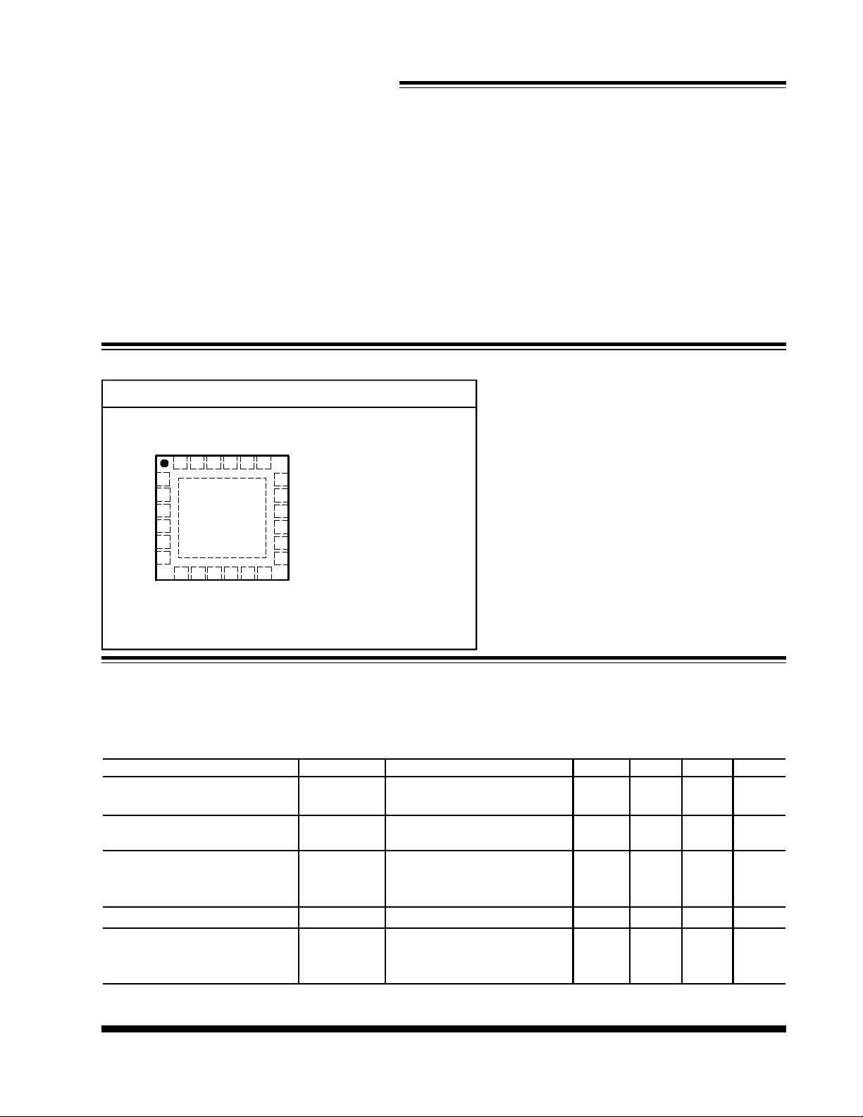
PACKAGE INFORMATION
24-LEAD PLASTIC MLPQ
LDRV2
DROOP
PVCC
LDRV1
2122
23
PGND(PAD)
8910 11
CS-2
CS+2
IOUT/IMAX
SW2
20
19
HDRV2
18
BST2
17
INREFOUT/POK
16
REFIN/EN
15
CSCOMP
14
13
FB
12
RT
VCOMP
JA
o
HDRV1
BST1
5VCC
AGND
ENBUS
CS+1
SW1
24
1
2
3
4
5
6
7
CS-1
ELECTRICAL SPECIFICATIONS
Unless otherwise specified, these specifications apply over 5Vcc = 5V, PVcc= 5V, V
BST-VSW
and TA = 0 to 70oC. Typical values refer to TA = 25oC. Low duty cycle pulse testing is used which keeps junction and
case temperatures equal to the ambient temperature.
5V
,PVCC Voltage Range V
CC
5VCC Supply Current (static)
PVCC Supply Current
(Dynamic)
V
Voltage Range V
BST
V
Supply Current
BST
((Dynamic))
Rev.1.9
05/06/08
CC
ICC (Static)
ICC
(Dynamic)
to V
BST
V
SW
BST
(Dynamic)
ENBUS=GND - 6.7
REFIN=ENBUS=5VCC,
Freq=200Khz per phase
C
=2200PF
LOAD
REFIN=ENBUS=5VCC,
Freq=200Khz per phase
C
=2200PF
LOAD
www.nexsem.com
4.5 5 5.5 V
4.5 5 5.5 V
=5V, ENBUS=HIGH,
mA
4.4 mA
mA4.5
2
Page 3
NEXSEM
PARAMETER
SYM
TEST CONDITION
MIN
TYP
MAX
UNITS
Under Voltage, Vcc &
ENBUS
VCC-Hysteresis
VCC_Hyst
V
BUS
Rising
Reference Voltage
Oscillator (Rt)
Amplifiers(CSCOMP)
Output Current Source
5
mA
SS (Internal )
POK/INFEROUT
Ldrv going Low to Hdrv going
NX2420
VCC-Threshold VCC_UVLO VCC Rising
ENBUS Threshold
ENBUS Hysteresis 80 mV
Ref Voltage V
Ref Voltage line regulation 0.2 %
Frequency for each phase Fs Rt=100kohm 400 KHz
Ramp-Amplitude Voltage V
Ramp Peak 2.2 V
Ramp Valley 1.18 V
Max Duty Cycle 200Khz/Phase 97 %
Min Duty Cycle 0 %
Transconductance
Open Loop Gain 50 65 dB
Transconductance 1600 umoh
Voltage Mode Error
Open Loop Gain 50 dB
Input Offset Voltage Vio_v 0 mV
Output Current Sink 5 mA
Output HI Voltage Vcc-1.5 V
Output LOW Voltage 0.5 V
REF
RAMP
4.5V<5Vcc<5.5V
4.1 V
0.4 V
0.82 V
0.592
1.02 V
V
Soft Start time Tss 400Khz/Phase 2.5 mS
Threshold VFB Rising 73 %V
Hysteresis 5 %
POK Voltage I
High Side Driver
(CL=4700pF)
Output Impedance , Sourcing
Current
Output Impedance , Sinking
Current
Rise Time THdrv(Rise) 10% to 90% 19 ns
Fall Time THdrv(Fall) 90% to 10% 18.5 ns
Deadband Time Tdead(L to
Low Side Driver
(CL=10000pF)
Output Impedance, Sourcing
Current
Output Impedance, Sinking
Current
Rev.1.9
05/06/08
R
(Hdrv)
source
R
(Hdrv)
sink
H)
R
(Ldrv) I=200mA 1 ohm
source
R
(Ldrv) I=200mA 0.5 ohm
sink
www.nexsem.com
=5mA(sourcing) 1.191 1.215 1.24 V
OUT
I=200mA
I=200mA
High, 10%-10%
1
0.7
40 ns
ohm
ohm
P
3
Page 4
NEXSEM
PARAMETER
SYM
TEST CONDITION
MIN
TYP
MAX
UNITS
Amplifier(CS+, CS-)
Source(Droop)
OVP Threshold
FB UVLO Threshold
REFIN VOLTAGE
NX2420
Rise Time TLdrv(Rise) 10% to 90% 34 ns
Fall Time TLdrv(Fall) 90% to 10% 18 ns
10 nsDeadband Time Tdead(H to L)SW going Low to Ldrv going
High, 10% to 10%
Propagation Delay Tdealy(H) IN going High to Ldrv going
Low
Current Sense
Input Offset Voltage -2 2 mV
Voltage Gain 29.7 30 30.3 V/V
Droop Voltage Current
14
ns
Droop Voltage Current Source 10 uA
OVP Threshold percent of Vp 130 %
FB UVLO Threshold percent of Vp 70 %
REFIN Voltage Range 0.4 2.5 V
Disable Voltage Threshold 0.3 0.35 0.4 V
Threshold Enable Internal
Reference
V(IOUT)=0.6V, feedback
resistor=10k,
Rdroop=60kohm
75 %VCC
Rev.1.9
05/06/08
www.nexsem.com
4
Page 5
NEXSEM
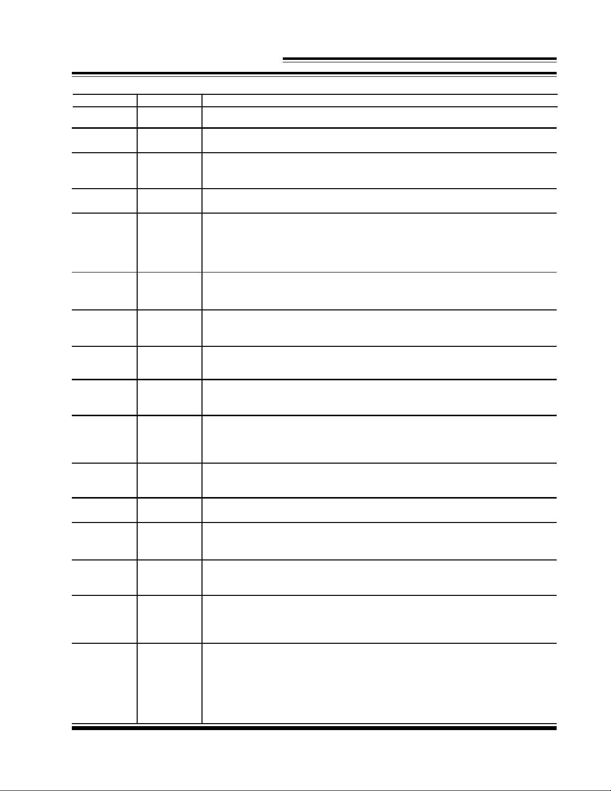
PIN DESCRIPTIONS
PIN # SYMBOL PIN DESCRIPTION
1
HDRV1
High side gate driver for Channel 1.
NX2420
2
3
4
5
6
7
8
9
10
BST1
5VCC
AGND
ENBUS
CS+1
CS-1
CS-2
CS+2
IOUT/IMAX
Bootstrap supply for Channel 1.
IC’s supply voltage. This pin biases the internal logic circuits. A minimum 1uF
ceramic capacitor is recommended to connect this pin to ground plane.
Controller analog ground pin.
This pin is used to program the under voltage lockout of the bus supply. A resistor
divider from the bus voltage to this pin programs the under voltage lockout. When
the voltage of this pin is greater than 0.8V, the bus voltage is assumed in operation.
The pin has a 10% hysterisis.
Positive input of the channel 1 differential current sense amplifiers. It is connected
directly to the RC junction of the respective phase’s output inductor.
Negative input of the channel 1 differential current sense amplifiers. It is connected directly to the negative side of the respective phase’s output inductor.
Negative input of the channel 2 differential current sense amplifiers. It is connected directly to the negative side of the respective phase’s output inductor.
Positive input of the channel 2 differential current sense amplifiers. It is connected
directly to the RC junction of the respective phase’s output inductor.
This pin indicates average output current level and sets OCP threshold using a
resistor from this pin to ground. A no more than 1nF ceramic capacitor is recommended to connect this pin to ground plane to filter the noise on this pin.
Rev.1.9
05/06/08
11
12
13
14
15
16
RT
VCOMP
FB
CSCOMP
REFIN/EN
INREFOUT/
POK
This pin programs the internal oscillator frequency using a resistor from this pin to
ground. The frequency of each phase is 1/2 of this frequency.
This is the output pin of the error amplifier.
This pin is the error amplifier inverting input. It is connected to the output voltage via
a voltage divider.
The output of the transconductance op amp for current balance circuit. An
external RC is connected from this pin to GND to stabilize the current loop.
External reference input. If pull-up to >75%VCC, internal reference is used. If driven
by an external voltage ranged from 0.4V to 2.5V, external reference is used with
slew rate following SS rate. If REFIN is below 0.4V, device is disabled.
This pin has dual functions. When FB pin is below 75% of internal 0.6V reference,
this pin is held low. When FB reaches above this threshold, this pin is tied to an
internal 1.25V reference, allowing it to be used as a reference for any external op
amp circuitry as well as an indicator of power OK. This pin can not be connected
directly to an output capacitor. An RC network is needed which also provides a slow
ramp up of the reference for the external op amp.
www.nexsem.com
5
Page 6
NEXSEM
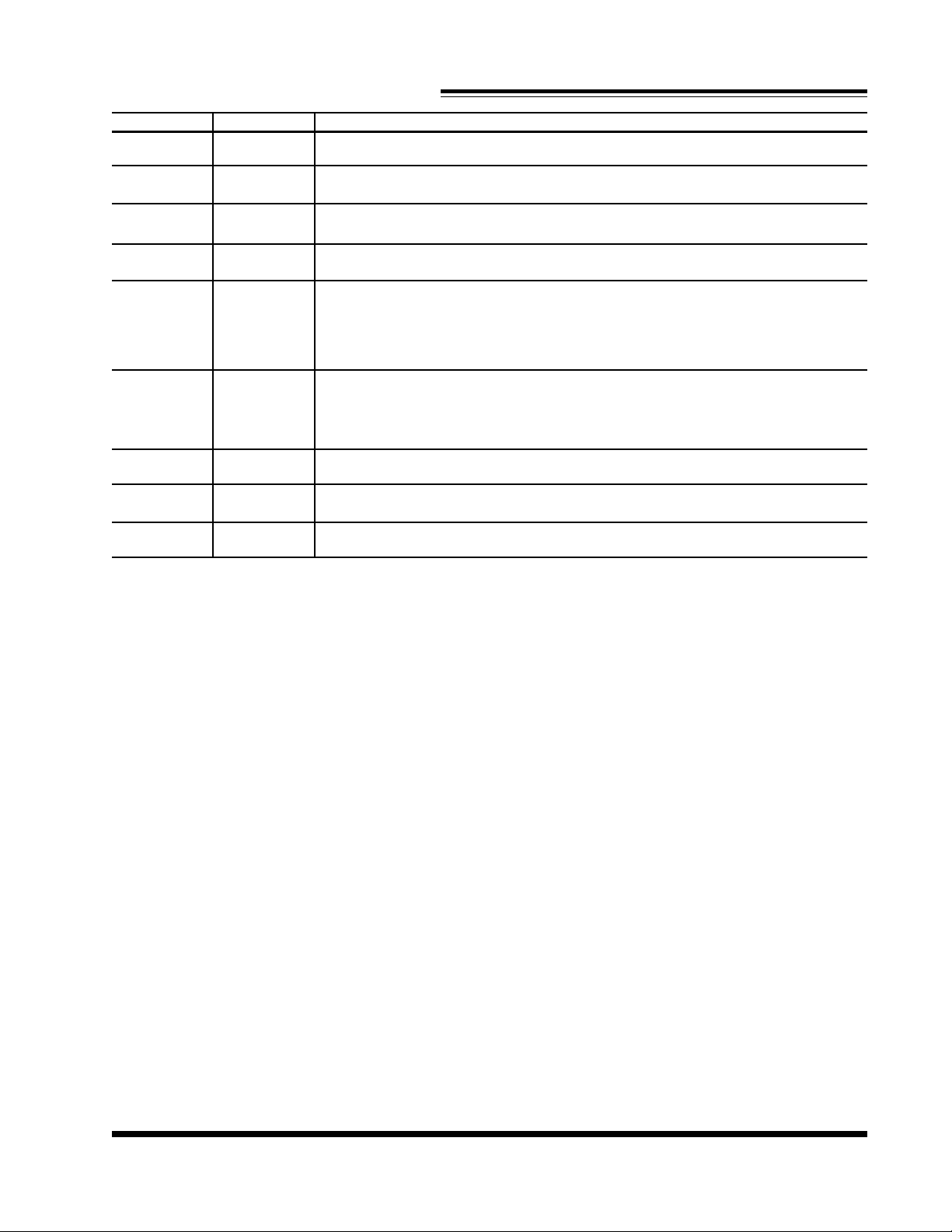
PIN # SYMBOL PIN DESCRIPTION
17
BST2
Bootstrap supply for Channel 2.
NX2420
18
19
20
21
22
23
24
PAD
HDRV2
SW2
LDRV2
DROOP
PVCC
LDRV1
SW1
PGND
High side gate driver for Channel 2.
Switch node for Channel2.
Low side gate driver for Channel 2.
A resistor from this pin to ground programs an internal current source that is fed
into the FB pin. This current source is proportional to the output current of the
regulator. The product of this current times the external resistor RFB provides a
droop voltage.
This pin provide the supply voltage for the lower MOSFET drivers. A high frequency ceramic 1uF X5R must be placed close to this pin and tied to PGND to
provide peak current needed for low side MOSFETs.
Low side gate driver for Channel 1.
Switch node for Channel 1.
This is the ground connection for the power stage of the controller.
Rev.1.9
05/06/08
www.nexsem.com
6
Page 7
NEXSEM
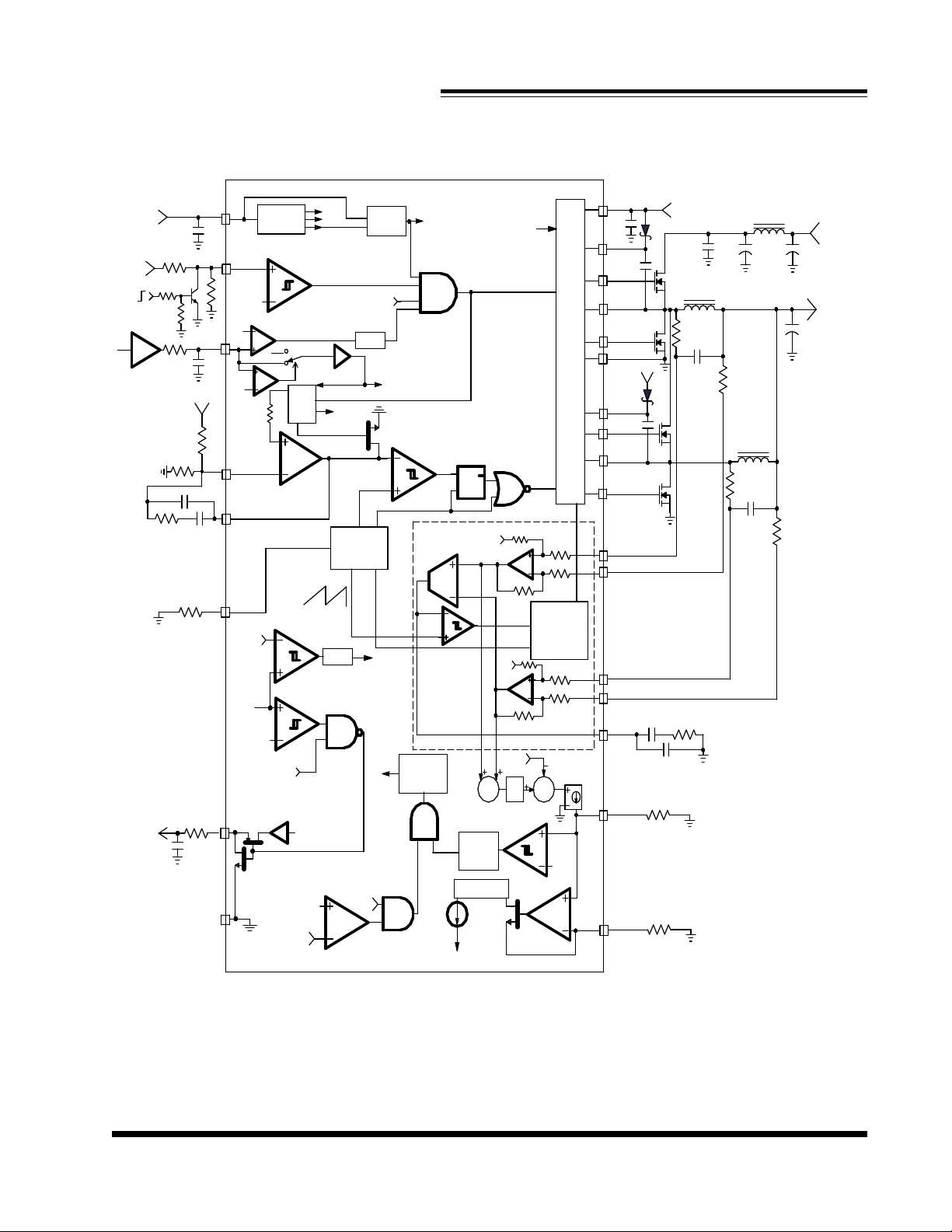
BLOCK DIAGRAM
NX2420
+5V
+12V
OFF
ON
DAC
5VCC
Enbus
REFIN/EN
VOUT
FB
VCOMP
Rt
INREFOUT/POK
AGND
0.82/0.74
0.4V
75%
VCC
Vp*130%
FB
Vp*75%
SS_finished
Bias
generator
0.6V
Digital
start
Vp*70%
1.25V
FB
0.6V
1.6V
1.25V
SS_finish
Dis_EA
ramp1
Two phase
OSC
ramp2
FILTER
SS_FINISHED
Hiccup
FILTER
Hiccup
UVLO
Vp
Set1
set2
OVP
UVLO
Hiccup
Logic
K=30
OVP
start
R
Q
S
KR
V1.25
CS01
CS02
Slave channel control
6 Cycles
filter
Current Mirror
FB
KR
V1.25
KR
V1.25
÷
Σ
2
FET
driver
R
R
PWM control
logic
and driver
KR
R
R
gm=0.04mA/V
Σ
1.25V
PVCC
BST1
DrvH1
SW1
DrvL1
PGND
+5V
BST2
DrvH2
SW2
DrvL2
CS+1
CS-1
CS+2
CS-2
CScomp(SS/EN)
IOUT/IMAX
DROOP
+5V
+12V
VOUT
+1.2V/50A
Rev.1.9
05/06/08
Figure 2 - block diagram of NX2420
www.nexsem.com
7
Page 8
NEXSEM
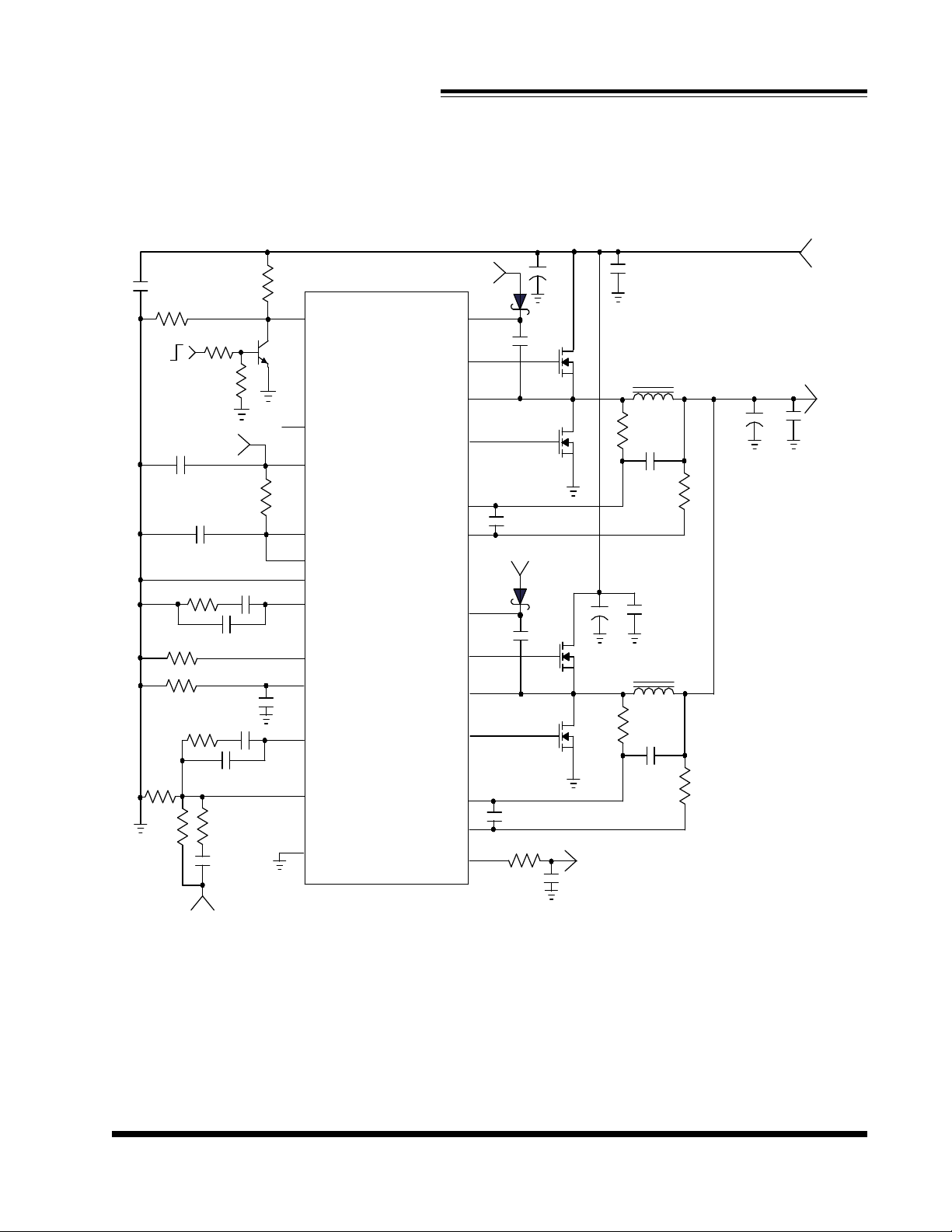
Demoboard design and waveforms
NX2420
sdfd
0.1uF
1k
ON
13.3k
10k
OFF
1uF
110k
63.4k
1uF
432
3.65k
10k
10k
+5V
2.2n
220p
4.12k
1n
10
220n
8.2n
10k
2N3904
21
22
3
15
4
14
11
10
1nF
12
13
5
ENBUS
DROOP
PVCC
5VCC
REFIN/EN
AGND
CSCOMP
RT
IOUT/IMAX
VCOMP
FB
PGND(PAD)
+5V
BST1
1
HDRV1
24
SW1
23
LDRV1
CS+1
CS-1
BST2
N X 2 4 2 0
HDRV2
SW2
LDRV2
CS+2
CS-2
INREFOUT/POK
16
2
BSC042N03S
6
1nF
7
17
18
19
20
BSC042N03S
9
1nF
8
+5V
1k
0.1u
0.1u
68uF
BSC119N03SG
640
68uF
BSC119N03SG
640
Ref for external circuitry
0.1u
2 x 10uF
2 x 4.7uF
2 x 1uF
0.47uH
1u
2 x 10uF
2 x 4.7uF
2 x 1uF
0.47uH
1u
640
640
3x
820uF
VIN
VOUT
4x
10uF
Rev.1.9
05/06/08
VOUT
Figure 3 - demoboard schematic of NX2420
www.nexsem.com
8
Page 9
NEXSEM
NX2420
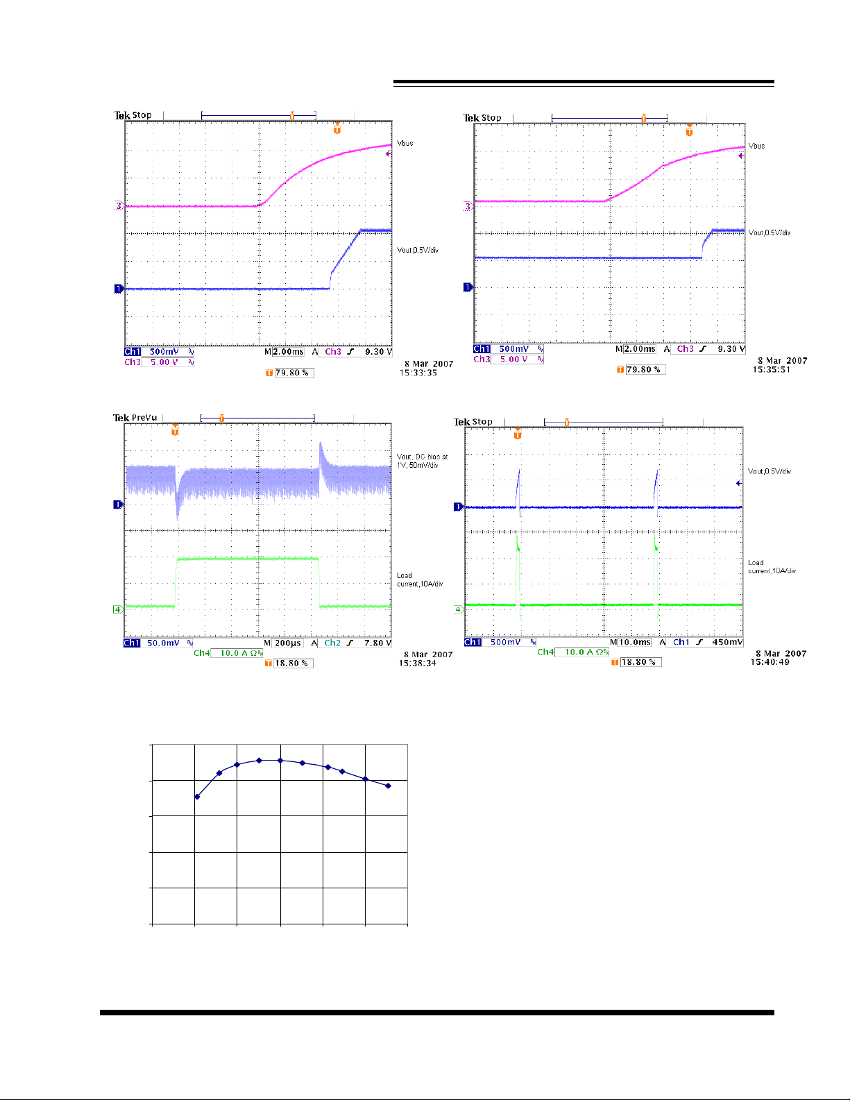
Figure 3 - Start up
Figure 5 - Transient response
NX2420 efficiency(%) vs Iout
85
80
Figure 4 - Prebias start up
Figure 6 - Over current protection
75
70
Efficiency(%)
65
60
0 10 20 30 40 50 60
Figure 7: Efficiency
Rev.1.9
05/06/08
Iout(A)
www.nexsem.com
9
Page 10
NEXSEM
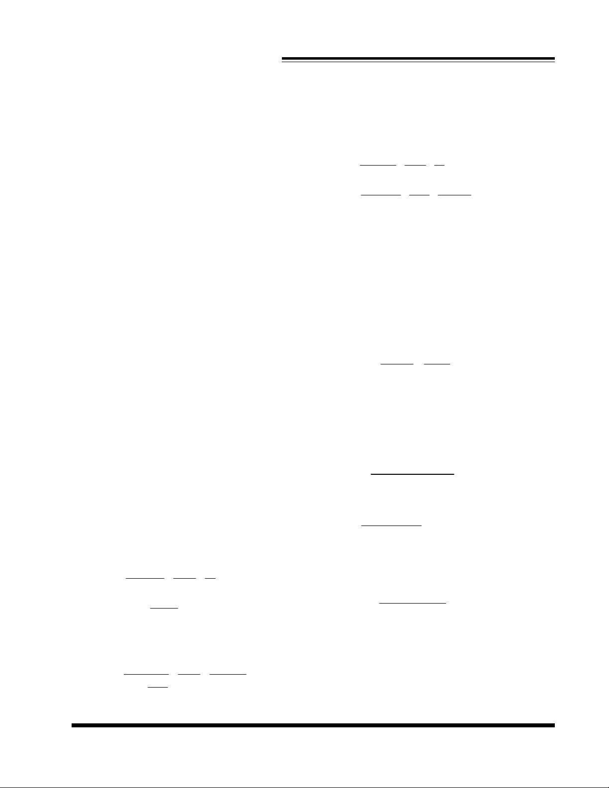
RIPPLEINS
1
IVF
12V400kHz
L=0.54uH
=3.97A
ESR=3.022m
==Ω
ERIPPLE
7m3.97A
12mV
SRIPPLE
NX2420
APPLICATION INFORMATION
Symbol Used In Application Information:
VIN - Input voltage
VOUT - Output voltage
IOUT - Output current
DVRIPPLE - Output voltage ripple
FS - Operation frequency for each channel
DIRIPPLE - Inductor current ripple
Design Example
The following is typical application for NX2420.
VIN = 12V
VOUT=1.2V
IOUT=50A
IOUT_max=60A
DVRIPPLE <=12mV
DVDROOP<=120mV @30A step
FS=400kHz
Phase number N=2
Output Inductor Selection
The selection of inductor value is based on inductor ripple current, power rating, working frequency and
efficiency. Larger inductor value normally means smaller
ripple current. However if the inductance is chosen too
large, it brings slow response and lower efficiency. Usually the ripple current ranges from 20% to 40% of the
output current. This is a design freedom which can be
decided by design engineer according to various application requirements. The inductor value can be calculated by using the following equations:
V-VV
L=
∆×
where k is between 0.2 to 0.4.
Select k=0.2, then
L=
OUT
INOUT OUT
OUT
∆
I=k
RIPPLE
12V-1.2V1.2V1
0.2
××
I
OUTPUT
N
50A
×
2
××
...(1)
OUT
Choose inductor from Vishay IHLP_5050FD-01
with L=0.68uH DCR=1.4mΩ.
Current Ripple is recalculated as
V-VV
I=
∆××
RIPPLE
INOUT OUT
LVF
OUTINS
12V-1.2V1.2V1
0.68uH12V400kHz
××=
1
...(2)
Output Capacitor Selection
Output capacitor value is basically decided by the
output voltage ripple, capacitor RMS current rating and
load transient.
Based on Voltage Ripple
For electrolytic, POSCAP bulk capacitor, the ESR
(equivalent series resistance) and inductor current typically determines the output voltage ripple.
V
∆
tiple capacitors in parallel are better than a big capacitor. For example, for 12mV output ripple, SANYO OSCON capacitors 2R5SEPC1000MX(1000uF 7mΩ) are
chosen.
mined by the number of capacitor instead of ESR
that the output voltage droop during the transient can
not meet the spec although ripple is small.
desire
If low ESR is required, for most applications, mul-
N
=
Number of Capacitor is calculated as
N
=
N =2.3
For ceramic capacitor, the current ripple is deter-
C
OUT
Typically, the calculated capacitance is so small
RIPPLE
I3.97A
∆
RIPPLE
ESRI
∆
Ω×
=
8FV
××∆
×∆
V
RIPPLE
I
∆
RIPPLE
12mV
...(3)
...(4)
...(5)
Rev.1.9
05/06/08
www.nexsem.com
10
Page 11

NEXSEM
DROOPTRAN
2
∆=×∆+×τ
OUTEFFcrit
ESRCifLL
OUTOUTEEOUT
crit
LL
2
=+×τ
EEEFFcrit
ESRCifLL
0.28H
=µ
7m1000F1.5us
2
1.78×∆=+×τ
NX2420
Based On Transient Requirement
Typically, the output voltage droop during transient
is specified as:
V<V∆∆ @ step load DI
During the transient, the voltage droop during the
transient is composed of two sections. One Section is
dependent on the ESR of capacitor, the other section is
a function of the inductor, output capacitance as well as
input, output voltage. For example, overshoot caused by
DISTEP transient load which is from high load to low load,
can be estimated as the following equation,if assuming
the bandwidth of system is high enough.
VESRI
tance of each capacitor if multiple capacitors are used
in parallel.
put inductor is smaller than the critical inductance, the
voltage droop or overshoot is only dependent on the ESR
of output capacitor. For low frequency capacitor such
as electrolytic capacitor, the product of ESR and capacitance is high and
transient spec is dependent on the ESR of capacitor.
capacitors in parallel. The number of capacitors can be
calculated by the following
overshootstep
where τ is the a function of capacitor, etc.
0ifLL
LI
τ=
L0.34uH
L
N
×∆
EFFstep
V
OUT
where
L
OUT
===
EFF
N2
ESRCVESRCV
==
crit
where ESRE and CE represents ESR and capaci-
The above equation shows that if the selected out-
In most cases, the output capacitors are multiple
ESRI
where
≤
EFFcrit
−×≥
0.68uH
××××
II
∆∆
stepstep
×∆
Estep
V2LCV
∆×××∆
tranEtran
2LC
≤ is true. In that case, the
V
OUT
V
OUT
××
STEP
OUT
...(6)
...(7)
...(8)
...(9)
0ifLL
LI
EFFstep
V
×∆
OUT
τ=
≤
EFFcrit
−×≥
...(10)
For example, assume voltage droop during transient
is 120mV for 30A load step.
If the OS-CON capacitors (1000uF, 7mΩ ) is used,
the critical inductance is given as
ESRCV
××
L
crit
7m1000F1.2V
Ω×µ×
The effective inductor value is 0.34uH which is bigger than critical inductance. In that case, the output voltage transient not only dependent on the ESR, but also
capacitance.
number of capacitors is
τ=−×
=−Ω×µ=
N
7m30A
=+
20.34H1000F120mV
×µ×µ×
=
The number of capacitors has to satisfied both ripple
and transient requirement. Overall, we can choose N=2.
It should be considered that the proposed equation is based on ideal case, in reality, the droop or overshoot is typically more than the calculation. The equation gives a good start. For more margin, more capacitors have to be chosen after the test. Typically, for high
frequency capacitor such as high quality POSCAP especially ceramic capacitor, 20% to 100% (for ceramic)
more capacitors have to be chosen since the ESR of
capacitors is so low that the PCB parasitic can affect
the results tremendously. More capacitors have to be
selected to compensate these parasitic parameters.
EEOUT
==
LI
0.34H30A
ESRI
Ω×
120mV
I
∆
step
30A
×∆
EFFstep
V
OUT
µ×
1.2V
Estep
V2LCV
∆×××∆
ESRC
EE
V
OUT
tranEFFEtran
1.2V
(1.5us)
×
2
Rev.1.9
05/06/08
www.nexsem.com
11
Page 12
NEXSEM
Gain= ... (11)
F= ... (12)
F ... (13)
NX2420
Control Loop Compensator Design
NX2420 can control and drive two channel synchronous bucks with 180o phase shift between each other.
One of two channels is called master, the other is called
slave. They are connected together by sharing the same
output capacitors. Voltage loop is designed to regulate
output voltage. In order to achieve the current balance in
these two synchronous buck converters, current loop
compensation network is employed to to make sure the
currents in slave is following the master.
Voltage Loop Compensator Design
Due to the double pole generated by LC filter of the
power stage, the power system has 180o phase shift ,
and therefore, is unstable by itself. In order to achieve
accurate output voltage and fast transient
response,compensator is employed to provide highest
possible bandwidth and enough phase margin. Ideally,
the Bode plot of the closed loop system has crossover
frequency between 1/10 and 1/5 of the switching frequency, phase margin greater than 50o and the gain crossing 0dB with -20dB/decade. Power stage output capacitors usually decide the compensator type. If electrolytic capacitors are chosen as output capacitors, type II
compensator can be used to compensate the system,
because the zero caused by output capacitor ESR is
lower than crossover frequency. Otherwise type III compensator should be chosen.
R
3
R
2
z
≈
p
Vout
R2
R1
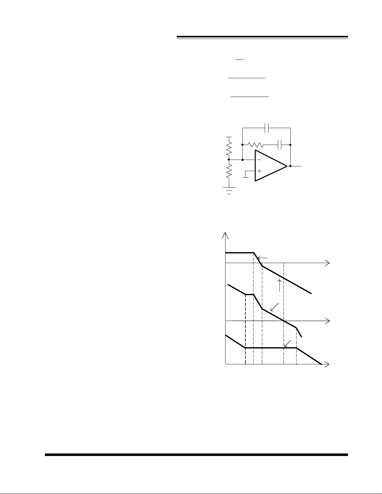
Figure 8 - Type II compensator
1
2RC
×π××
31
1
2RC
×π××
32
R3
Fb
Vref
C2
C1
power stage
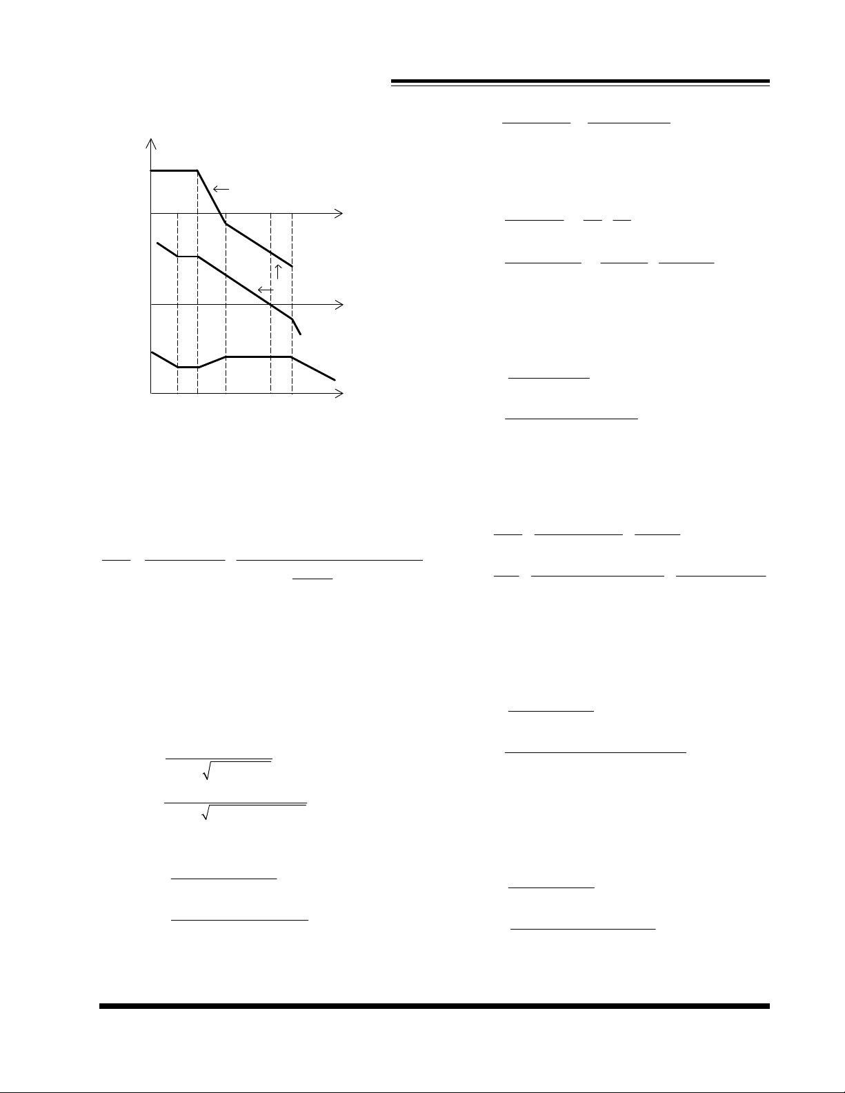
40dB/decade
Gain(db)
loop gain
20dB/decade
Ve
A. Type II compensator design
If the electrolytic capacitors are chosen as power
stage output capacitors, usually the Type II compensator can be used to compensate the system.
Type II compensator can be realized by simple RC
circuit without feedback as shown in figure 8. R3 and C1
introduce a zero to cancel the double pole effect. C2
introduces a pole to suppress the switching noise. The
following equations show the compensator pole zero location and constant gain.
Rev.1.9
05/06/08
Figure 9 - Bode plot of Type II compensator
For this type of compensator, FO has to satisfy
FLC<F
which has six electrolytic capacitors(1800uF, 13mΩ) and
<< FO and FO <=1/10~1/5F
ESR
Here a type II compensator is designed for the case
www.nexsem.com
compensator
F
F
LC
Z
F
ESRFO
Gain
P
F
s.
12
Page 13
NEXSEM
20.75uH10800uF
213m1800uF
R=10k
==Ω
=10k
=27.3k
××Ω
227.4k0.751.768kHz
p
F
27.4k400kHz
F ...(14)
F ...(15)
F ...(16)
F ...(17)
NX2420
two 1.5uH inductors.
1.Calculate the location of LC double pole F
and ESR zero F
F
=
LC
=
.
ESR
1
2LC
×π××
EFFOUT
1
×π××
1.768kHz
=
1
OUT
1
F
=
ESR
2ESRC
×π××
=
×π×Ω×
6.801kHz
=
LC
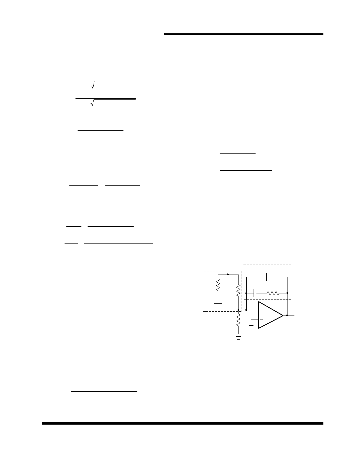
B. Type III compensator design
Sanyo OSCON and POSCAP, the frequency of ESR zero
caused by output capacitors is higher than the crossover frequency. In this case, it is necessary to compensate the system with type III compensator.
used as output capacitors. The system is compensated
with type III compensator. The following figures and equations show how to realize the this type III compensator
with electrolytic capacitors.
2.Set R2 equal to10kΩ and calculate R1.
×
2REF
1
V-V1.2V-0.6V
OUT REF
10k0.6V
Ω×
RV
3. Set crossover frequency FO=15kHz.
4.Calculate R3 value by the following equation.
V2FL
R=R
OSCOEFF
32
VESR
in
1V215kHz0.75uH
12V2.16m
×π××
××
×π××
Ω
Ω
the compensator.
Choose R3 =27.4kΩ.
5. Calculate C1 by setting compensator zero F
Z
at 75% of the LC double pole.
C=
1
=
1
2RF
×π××
3z
1
×π×Ω××
=4.4nF
For low ESR output capacitors, typically such as
In design example, six electrolytic capacitors are
1
×π××
2RC
42
1
×π×+×
2(RR)C
233
1
×π××
2RC
33
1
×
CC
4
CC
12
+
12
×π××
2R
=
Z1
=
Z2
=
P1
=
P2
where FZ1,FZ2,FP1 and FP2 are poles and zeros in
C2
Fb
Zf
C1
R4
Zin
Vout
R3
R2
C3
Ve
R1
Vref
Choose C1=4.7nF.
6. Calculate C2 by setting compensator pole
at half the swithing frequency.
C=
2
=
=30pF
1
RF
π××
3s
1
π×Ω×
Choose C2=33pF.
Rev.1.9
05/06/08
Figure 10 - Type III compensator
www.nexsem.com
13
Page 14
NEXSEM
[
]
42233
(1sRC)1s(RR)C
20.34uH2000uF
23.5m2000uF
R=10k
==Ω
=(-)
210k6.1kHz22.7kHz
=1.9nF
222.7kHz1.8nF
1V240kHz0.34uH10k3.92k
12V3.5m10k3.92k
×π××Ω×Ω
ΩΩ+Ω
20.756.1kHz5.62k
×π×××Ω
25.62k200kHz
power stage
LC
F
Gain(db)
loop gain
40dB/decade
F
ESR
20dB/decade
×
2REF
1
V-V1.2V-0.6V
OUT REF
10k0.6V
RV
Choose R1= 10kΩ.
3. Calculate C3 by setting FZ2 = F
C=(-)
3
111
2RFF
×π×
×π×Ω
×
2z2p1
111
×
Ω×
NX2420
and Fp1 =F
LC
ESR
.
compensator
P1
Z2
Z1
F
F
F
F
O
F
P2
Figure 11 - Bode plot of Type III compensator
The transfer function of type III compensator
is given by:
V
e
=×
VsR(CC)
OUT 221
1
×+
+××++×
CC
×
(1sR)1sRC
+××+×
21
433
CC
21
+
( )
Use the same power stage requirement as demo
board. The crossover frequency has to be selected as
FLC<F
1.Calculate the location of LC double pole F
and ESR zero F
, and usually FO<=1/10~1/5FS.
ESR<FO
.
ESR
F
=
LC
2LC
=
1
×π××
EFFOUT
1
LC
×π××
6.1kHz
=
F
ESR
22.7kHz
=
2ESRC
=
=
1
×π××
OUT
1
×π×Ω×
2.Set R2 equal to10kΩ.
Choose C3=1.8nF.
5. Calculate R3 by equation (13).
R
=
3
=
3.89k
=Ω
1
2FC
×π××
P13
1
×π××
Choose R3=3.92kΩ.
6. Calculate R4 by choosing FO=40kHz.
V2FLRR
R=
4
VESRRR
=
=5.73k
×π×××
OSCOEFF23
××
in23
+
××
Ω
Choose R4=5.62kΩ.
7. Calculate C2 with zero Fz1 at 75% of the LC
double pole by equation (11).
1
2FR
×π××
Z14
1
C
=
2
=
6.2nF
=
Choose C2=6.8nF.
8. Calculate C1 by equation (14) with pole Fp2 at
half the switching frequency.
C
=
1
=
141pF
=
1
2RF
×π××
4P2
1
×π×Ω×
Choose C1=150pF.
Rev.1.9
05/06/08
www.nexsem.com
14
Page 15
NEXSEM
Current Loop Compensator Design
NX2420
Power stage
Master
channel
Ramp for
slave channel
Compensation
D(s)
Current Sensing
Amplifier Gain
1
Vosc
d
s*L+Req
s*L+DCR
Rs*Cs*s+1
Inductor Current
sense
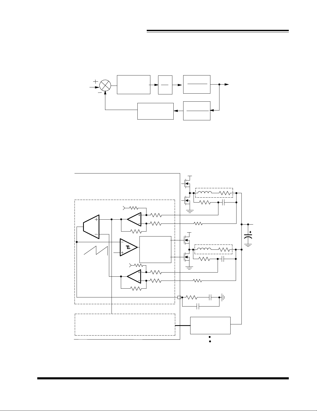
Figure 12 - Current loop control diagram
V
IN
Vbias
V
IN
PWM control
logic
and driver
Vbias
Vin
Rs
Rs
iL
master channel
L
Rs
Slave channel 1
L
Rs
DCR
Cs
DCR
Cs
V
OUT
Rev.1.9
05/06/08
CSCOMP
Slave channel control
Slave channel control
Rcc
C2
Slave channel
Figure 13 - Function diagram of current loop
www.nexsem.com
C1
15
Page 16
NEXSEM
L
DCR
S_ILL
VDCRi
=×
1
CF
=µ
S
DCRC
486
==Ω
S
DCRC
01101
004
.(.)
NX2420
Inductor Current Sensing
V
IN
Control &
Driver
Current
Sensing
Rs
L
Rs
i
L
DCR
V
OUT
Cs
V
S_IL
Amplifier
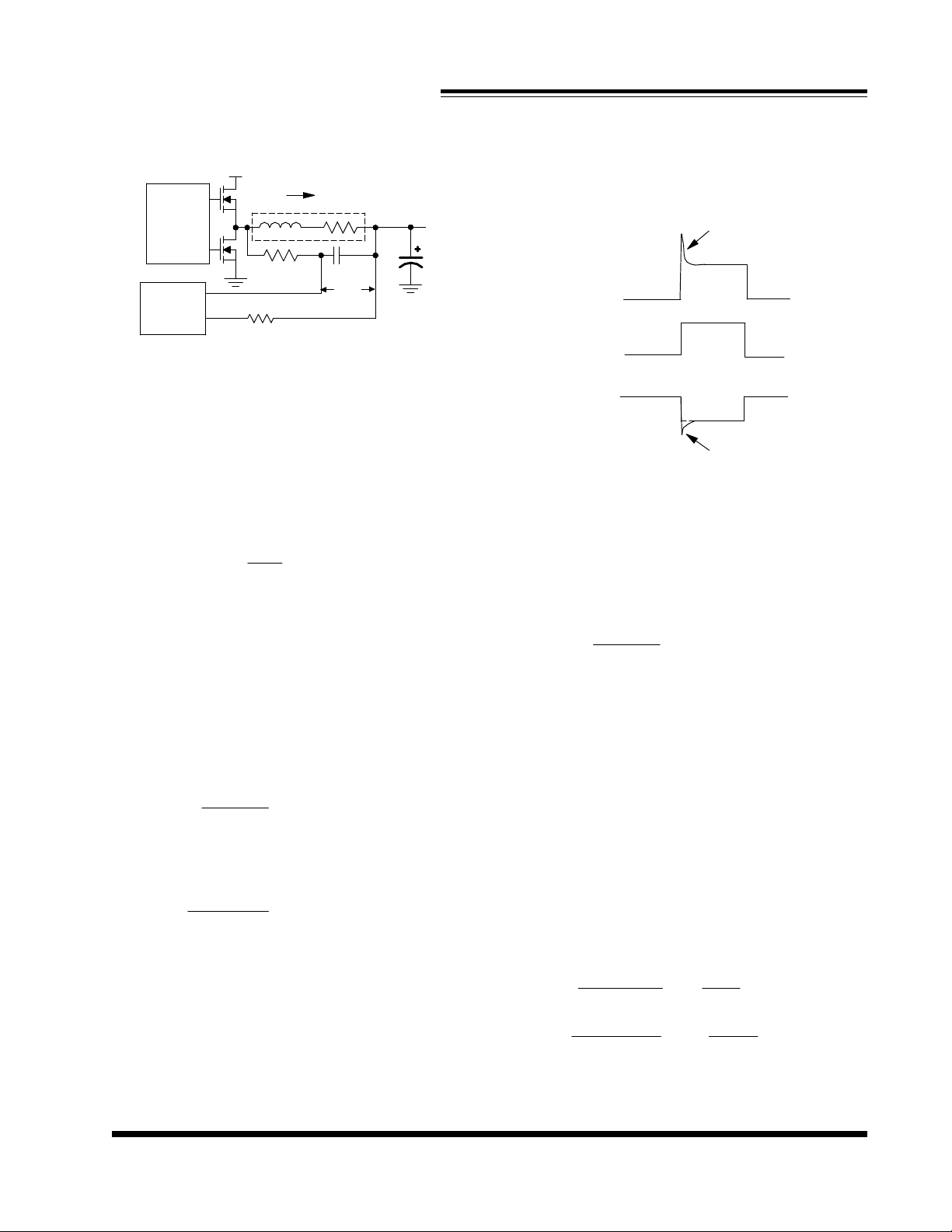
Figure 14 - Inductor current sensing using RC network.
The inductor current can be sensed through a RC
network as shown above. The advantage of the RC network is the lossless comparing with a resistor in series
with output inductor.
The selection of the resistor sensing network is
chosen by the following equation:
RC
×=
SS
...(18)
racy during the transient if droop function is required.
The illustration is shown in the following figure.
Overshoot caused
by inductor
V
S_IL
----Voltage accross
nonlinearity
the sensing
capacitor Cs
iL--- inductor current
Output voltage
with droop function
Droop misbehavoir
caused by
overshoot of V
S_IL
Figure 15 - Droop accuracy affected by the nonlinearity
of inductor.
If the above equation is satisfied, the voltage across
the sensing capacitor Cs will be equal to the inductor
current times DCR of inductor for all frequency domain.
If the sensing capacitor is chosen
S
CS must be X7R or COG ceramic capacitor.
The sensing resistor is calculated as
R
S
L
=
×
For example, for 0.68uH inductor with 1.4mΩ
DCR, we have
068
.H
R
S
µ
141
.mF
Ω×µ
In most of cases, the selection of sensing resistor based on the above equation will be sufficient. However, for some inductor such as toroid coiled inductor
with micrometal, even the product of sensing resistor
and capacitor is perfectly match with L/DCR, the voltage
across the capacitor still has overshoot due to the
nonlinearity of inductor. This will affect the droop accu-
In this case, the sensing resistor has to be chosen
R
S
L
≥
×
to compensate the overshoot. This selection only affects the small signal mode of current loop. For DC accuracy, there is no effect since the DC voltage across
the sensing capacitor will equal to the DCR times inductor current at DC load no matter what Rs is. In this example, Rs=620Ω.
RS value is preferred to be less than 400Ω in
NX2420's application, therefore we need to reiterate the
calculation, choose CS 2.2uF instead. RS value is finally
chosen as 301Ω .
Powe dissipation of Rs resistor is calculated as
followed:
(VV)V
−
P(R)D(D)
DS
=×+×−
=
INOUTOUT
=×+×−
121212
(V.V)(.V)
−
301301
.W
22
RR
SS
22
1
ΩΩ
The power rating of Rs should be over 0.04W.
Rev.1.9
05/06/08
www.nexsem.com
16
Page 17
NEXSEM
F.kHz
12
RCC
oosc
gVKDCR
229
K.
442
==Ω
430
=Ω
214
CnF
×π×
dson_con
dson_syn
R.m
=Ω
Current Loop Compensation
NX2420
R
eq
===
1
P
22068
L.H
×π××π×µ
74
.m
Ω
17
Slave channel
power stage
Current loop
compensation
Loop gain
for slave
channel
Fp1
Fzc Fpc
-20 dB
-20dB
0 DB
-40dB
Fo
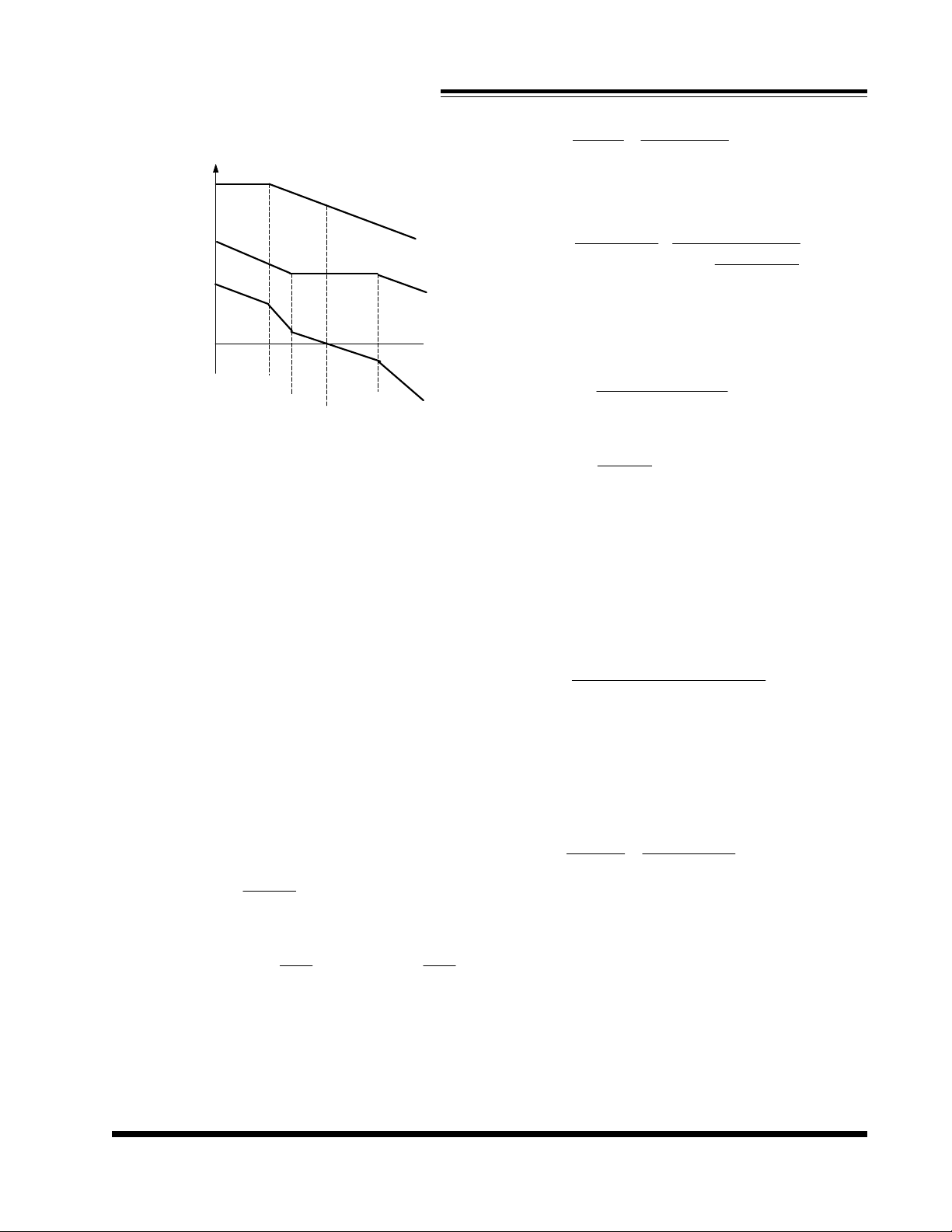
Figure 16 - Bode plot of current loop
The diagram and bode plot for current loop of
NX2420 is shown in above figures. The current signal
through inductor sensing is amplified by current sensing
differential amplifier. The amplified slave current signal
is compared with the amplified inductor current from
master channel (channel 1 for NX2420) through a
transconductance amplifier, the difference between channel current will change the output of transconductance
amplifier, which will compare with a internal ramp signal
and changes the duty cycle of slave channel buck converter. If the inductor are perfectly matched and the PWM
controller has no offset, the DC current in slave channel
will equal to the DC current of master channel (channel
1) due to the gain of current loop.
From the bode plot, the power stage has one pole
located at
R
FL=
1
P
eq
2
where Req is the equivalent resistor and it is given by
VV
RDCRRR
≈+×+×−
eqdson_condson_syn
R
is the Rdson of control FET and
OUTOUT
VV
ININ
1
R
is
the Rdson of synchronous FET. For this example,
74
eq
The pole is located as
The current compensation transfer function is
given as
1
sRCg
D(s)
=×
m
sCC
×+
( )
12
1
+××
cc
s
+×
1
cc
××
CC
+
12
It has one zero and one pole. The ideal is to
choose resistor Rcc to achieve desired loop gain such
as 50kHz. Rcc can be calculated as
2
FLV
R
×π×××
=
cc
mINC
×××
...(19)
where
60
k
⋅Ω
≈=
C
2
kR
Ω+
S
60kΩ and 2kΩ is the internal resistance for the current
sensing amplifier.
For fast response, we can set the current loop
cross-over frequency one and half times of voltage loop
cross-over frequency. Since the voltage loop cross-over
frequency is typically selected as 1/10 of switching frequency, we choose FO=50kHz.
2500681
R
cc
×π××µ×
161222914
.mA/VV..m
kHz.HV
×××Ω
Select
R
cc
.
The selection of capacitor C1 is such that the zero
of compensation will cancel the pole of power stage,
therefore,
L.H
===
1
RR.m
×Ω×Ω
eqcc
068
µ
74430
Typically, the capacitor C1 is so big that the current loop may start slowly during the start up. Therefore, smaller capacitor can be selected. However, the
selected capacitor can not reduce too much to cause
phase droop.
Select C1=220nF.
The capacitor C2 is an option and it is used to
filter out the switching noise. C2 can be calculated as
Rev.1.9
05/06/08
www.nexsem.com
17
Page 18
NEXSEM
185
C.nF
40000000
OUTDROOPINLOADLL
VIRIR
R3m
==Ω
LOAD
LOADIN
DCRIR
0.660k1.4m20A10k
ΩΩ××Ω
11
===
2
RFkHz
π××π×Ω×
ccS
Select C2=2.2nF.
Frequency Selection
The frequency can be set by external Rt resistor.
The relationship between frequency per phase and RT
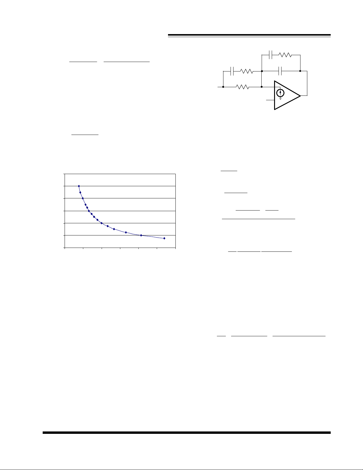
pin around 400kHz is shown as follows.
RF≈
T
1200
S
Frequency(kHz) vs Rt(kohm)
430400
...(20)
NX2420
VOUT
IN
R
Figure 18 - Output voltage droop funciton
∆=×=∆× ...(21)
Where RLL is desired load impedance. For example,
if we want Vout droops 60mV @ 20A,
60mV
LL
20A
FB
DROOP
I
V
P
COMP
Error Amplifer
1000
800
600
400
Frequency(kHz)
200
0
0 50 100 150 200 250 300
Rt(kohm)
Figure 17 - Frequency vs Rt chart
Output Voltage Droop Operation
The effective output impedance of the controller must
be adjusted to maximize the output voltage fluctuation
range. A program resistor attached to the Droop pin
R
will program this value. The function works by an
DROOP
internal current source connected to the FB pin. This
current flows output of the FB pin and through the Rin
resistance from the FB pin to the output.
This current source is a function of the sensed
output current. As the output current increases, the droop
current will increase and causes the output voltage
todroop proportionately. The droop current is programmed
by a resistor attached to the Droop pin. The value of the
resistor is chosen as follows.
V(IOUT)
=
R
DROOP
60kDCR
0.6I
×××
Ω
2kR2
Ω+
S
R
DROOP
...(22)
I
DROOP
=
Combine equation 22 and 23,
R
DROOP
0.660k
=
22kRV
Ω
Ω+∆
SOUT
...(23)
Where DCR is the sense resistor or the DCR of
the output inductor. RS is the current sensing matching
resistor when using DCR sensing method. I
LOAD
is the
load current. RIN is the input DC resistor of the master
phase compensator which connect FB pin and VOUT.
For example, to have the DV
=60mV when the load
OUT
current is 20A, DCR is 1.4mΩ, RIN is 10kΩ, RS is 620Ω.
R
=Ω
=××
DROOP
22k0.62k60mV
Ω+Ω
32k
Choose R
DROOP
= 32kΩ.
Over Voltage Protection
Over voltage protection is achieved by sensing the
output voltage through resistor divider. The sensed voltage on FB pin is compared with 130%*V
the OVP signal.
to generate
REF
Rev.1.9
05/06/08
www.nexsem.com
18
Page 19
NEXSEM
0
D
(
)
Iout
OCP
1.25V21
0.04mA/V60kDCRI
75
I.A
gateHGATEHGSLGATELGSS
P(QVQV)F
=×+××
P=I(1D)RK
×−××
Over Current/Short Circuit Protection
The converter will go into hiccup mode if the
output current reaches a programmed limit I
determined by the resistor value R
2kR
Ω+
R
=×××
OCP
Where I
level, RS is the current sensing matching resistor when
using DCR sensing method.
is the desired over current protection
ocp
S
Ω
Input Filter Selection
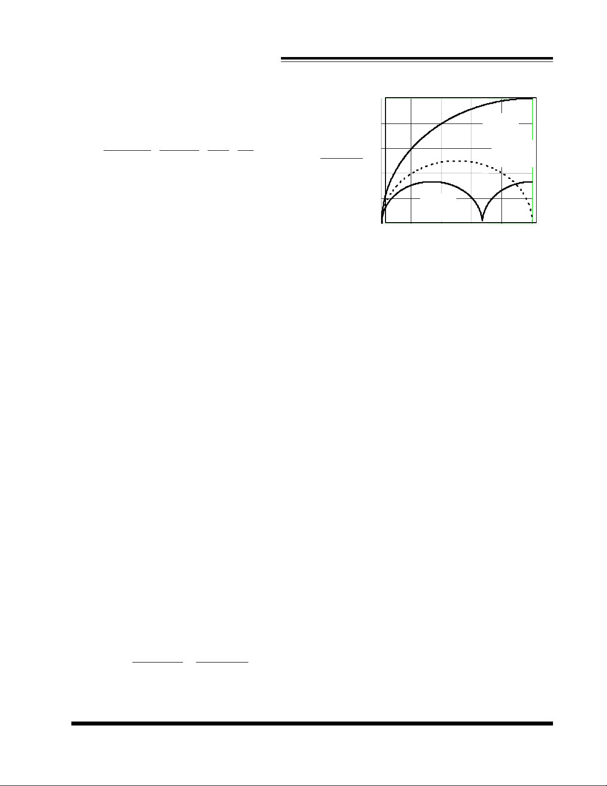
The selection criteria of input capacitor are voltage
rating and the RMS current rating. For conservative consideration, the capacitor voltage rating should be 1.5
times higher than the maximum input voltage. The RMS
current rating of the input capacitor for multi-phase converter can be estimated from the above Figure 19.
First, determine the duty cycle of the converter (VO/
VIN). The ratio of input RMS current over output current
can be obtained. Then the total input RMS current can
be calculated. From this figure, it is obvious that a multiphase converter can have a much smaller input RMS
current, which results in a lower amount of input capacitors that are required.
For example, Vin=12V, Vout=1.2V. The duty cycle
is D=Vout/Vin=1.2/12=10%. From the figure, for two
phase, the normlized RMS current is
0.2*Iout=0.2*50A=10A.
A combination of ceramic and electrolytic(SANYO
WG or WF series) or OSCON type capacitors can
achieve both ripple current capability together with having enough capacitance such that input voltage will not
sag too much. In this application, one OSCON
SVPC180M(180uF, 16V, 2.8A) and three 10uF X5R ceramic capacitors are selected.
A 1uH input inductor is recommended to slow down
the input current transient. Suppose power stage efficiency is 0.8, then input current can estimated by
IV
INPUT
In this application, Coilcraft DO3316P_102HC with
RMS rating 10A is chosen.
V.V
η××
IN
×
OUTOUT
===
6012
at pin IOUT/IMAX.
ocp
A.V
×
0812
...(24)
NX2420
OCP
RMS
Power MOSFETs Selection
MOSFETs for each channels. The selection of
MOSFETs is based on maximum drain source voltage,
gate source voltage, maximum current rating, MOSFET
on resistance and power dissipation. The main consideration is the power loss contribution of MOSFETs to
the overall converter efficiency. In this design example,
eight NTD60N02 are used. They have the following parameters: VDS=25V, ID =62A,R
loss:conduction loss, switching loss and gate driver loss.
ing the gate capacitor and is dissipated in driver circuits.
It is proportional to frequency and is defined as:
charge,QLGATE is the low side MOSFETs gate charge,VHGS
is the high side gate source voltage, and V
the low side gate source voltage. This power dissipation
should not exceed maximum power dissipation of the
driver device.
0.5
0.4
0.3
INI
0.2
0.1
0
Figure 19 - Normalized input RMS current vs.
The NX2420 requires two N-Channel power
There are three factors causing the MOSFET power
Gate driver loss is the loss generated by discharg-
where QHGATE is the high side MOSFETs gate
Conduction loss is simply defined as:
P=IDR
HCONOUTDS(ON)
LCONOUTDS(ON)
P=PP
TOTALHCONLCON
2
2
Three
phase
0.1 0.2 0.3
duty cycle.
DSON
×××
+
Singlephase
Two
phase
=12mΩ,Q
K
...(26)
0.4 0.5
=9nC.
GATE
...(25)
is
LGS
Rev.1.9
05/06/08
www.nexsem.com
19
Page 20

NEXSEM
SWINOUTSWS
PVITF
=××××
SW
T
S
dt1024T
1024
F
NX2420
Where the RDS(ON) will increases as MOSFET junction temperature increases, K is RDS(ON) temperature
dependency and should be selected for the worst case.
Conduction loss should not exceed package rating or
overall system thermal budget.
Switching loss is mainly caused by crossover conduction at the switching transition. The total switching
loss can be approximated.
1
2
is the sum of TR and TF which can be found in
mosfet datasheet, IOUT is output current, and FS is switching frequency. Swithing loss PSW is frequency depen-
dent.
...(27)
Soft Start and Enable Signal Operation
The NX2420 will start operation only after 5VCC
and PVCC have reached their threshold voltages and
ENBUS have been enabled. The ENBUS pin can be programmed to turn on the converter at any input voltage.
The ENBUS pin has a threshold voltage of 0.8V.
Once the converter starts, there is a soft start sequence of 1024 steps between 0 and Vp. The ramp rate
is determined by the switching frequency.
dVV
OO
T
startup
=
=
...(28)
×
...(29)
S
The softstart time is calculated as followed:
Layout Considerations
The layout is very important when designing high
frequency switching converters. Layout will affect noise
pickup and can cause a good design to perform with
less than expected results.
There are two sets of components considered in
the layout which are power components and small signal components. Power components usually consist of
input capacitors, high-side MOSFET, low-side MOSFET,
inductor and output capacitors. A noisy environment is
generated by the power components due to the switching power. Small signal components are connected to
sensitive pins or nodes. A multilayer layout which in-
cludes power plane, ground plane and signal plane is
recommended .
Layout guidelines:
1. First put all the power components in the top
layer connected by wide, copper filled areas. The input
capacitor, inductor, output capacitor and the MOSFETs
should be close to each other as possible. This helps to
reduce the EMI radiated by the power loop due to the
high switching currents through them.
2. Low ESR capacitor which can handle input RMS
ripple current and a high frequency decoupling ceramic
cap which usually is 1uF need to be practically touching
the drain pin of the upper MOSFET, a plane connection
is a must.
3. The output capacitors should be placed as close
as to the load as possible and plane connection is required.
4. Drain of the low-side MOSFET and source of
the high-side MOSFET need to be connected thru a plane
ans as close as possible. A snubber nedds to be placed
as close to this junction as possible.
5. Source of the lower MOSFET needs to be connected to the GND plane with multiple vias. One is not
enough. This is very important. The same applies to the
output capacitors and input capacitors.
6. Hdrv and Ldrv pins should be as close to
MOSFET gate as possible. The gate traces should be
wide and short. A place for gate drv resistors is needed
to fine tune noise if needed.
7. Vcc capacitor, BST capacitor or any other bypassing capacitor needs to be placed first around the IC
and as close as possible. The capacitor on comp to
GND or comp back to FB needs to be place as close to
the pin as well as resistor divider.
8. The output sense line which is sensing output
back to the resistor divider should not go through high
frequency signals.
9. All GNDs need to go directly thru via to GND
plane.
10. The feedback part of the system should be
kept away from the inductor and other noise sources,
and be placed close to the IC.
11. In multilayer PCB, separate power ground and
Rev.1.9
05/06/08
www.nexsem.com
20
Page 21
NEXSEM
analog ground. These two grounds must be connected
together on the PC board layout at a single point. The
goal is to localize the high current path to a separate
loop that does not interfere with the more sensitive analog control function.
12. Inductor current sense line should be connected
directly to the inductor solder pad.
Typical Application with external reference
NX2420
DAC
C30
R36
R32
ON
R46
R37
VOUT
R33
R34
OFF
C32
R44
R35
R47
R48
+5V
C33
C35
R45
C36
C34
R31
2N3904
C37
5
ENBUS
21
DROOP
22
PVCC
3
5VCC
15
REFIN/EN
4
AGND
14
CSCOMP
11
RT
10
IOUT/IMAX
12
VCOMP
13
FB
PGND(PAD)
+5V
2
BST1
1
HDRV1
24
SW1
23
LDRV1
CS+1
6
7
CS-1
17
BST2
N X 2 4 2 0
INREFOUT/POK
HDRV2
SW2
LDRV2
CS+2
CS-2
18
19
20
9
8
16
C42
C43
+5V
R27
C31
C21
C10
C11
C20
Q1
L1
R43
Q2
Q3
Q4
C41
C25 C24
L2
R42
C40
Ref for external circuitry
R41
R40
C27
VIN
C22C23
C26
VOUT
Rev.1.9
05/06/08
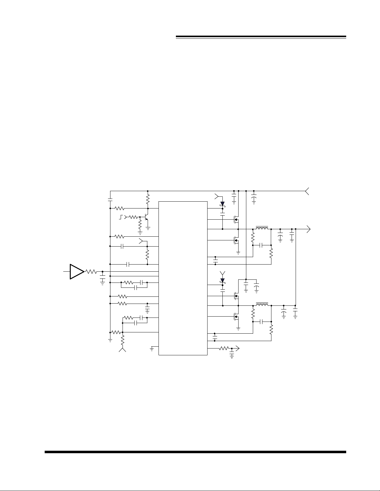
Figure 20 - Typical application of NX2420 with external reference
www.nexsem.com
21
Page 22
NEXSEM
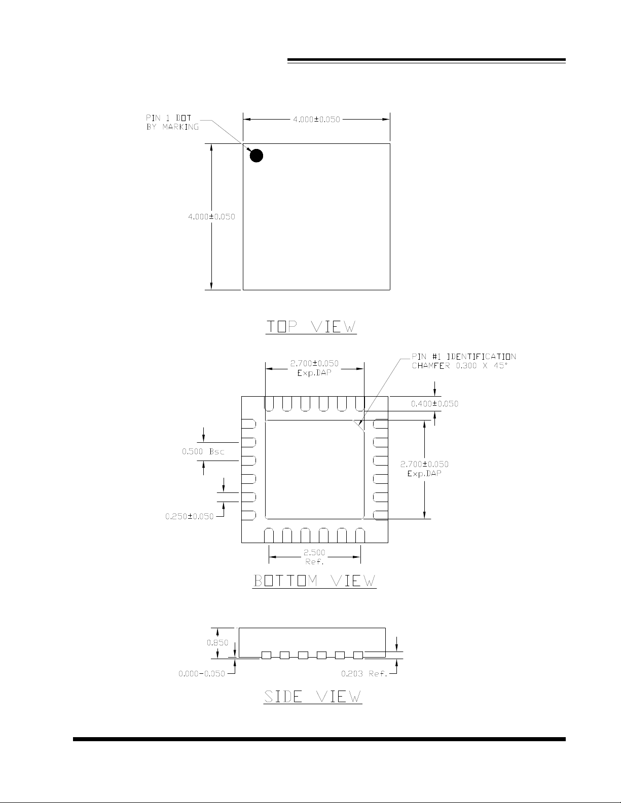
MLPQ 24 PIN 4 x 4 PACKAGE OUTLINE DIMENSIONS
NX2420
Rev.1.9
05/06/08
NOTE: ALL DIMENSIONS ARE DISPLAYED IN MILLIMETERS.
www.nexsem.com
22
Page 23
NEXSEM
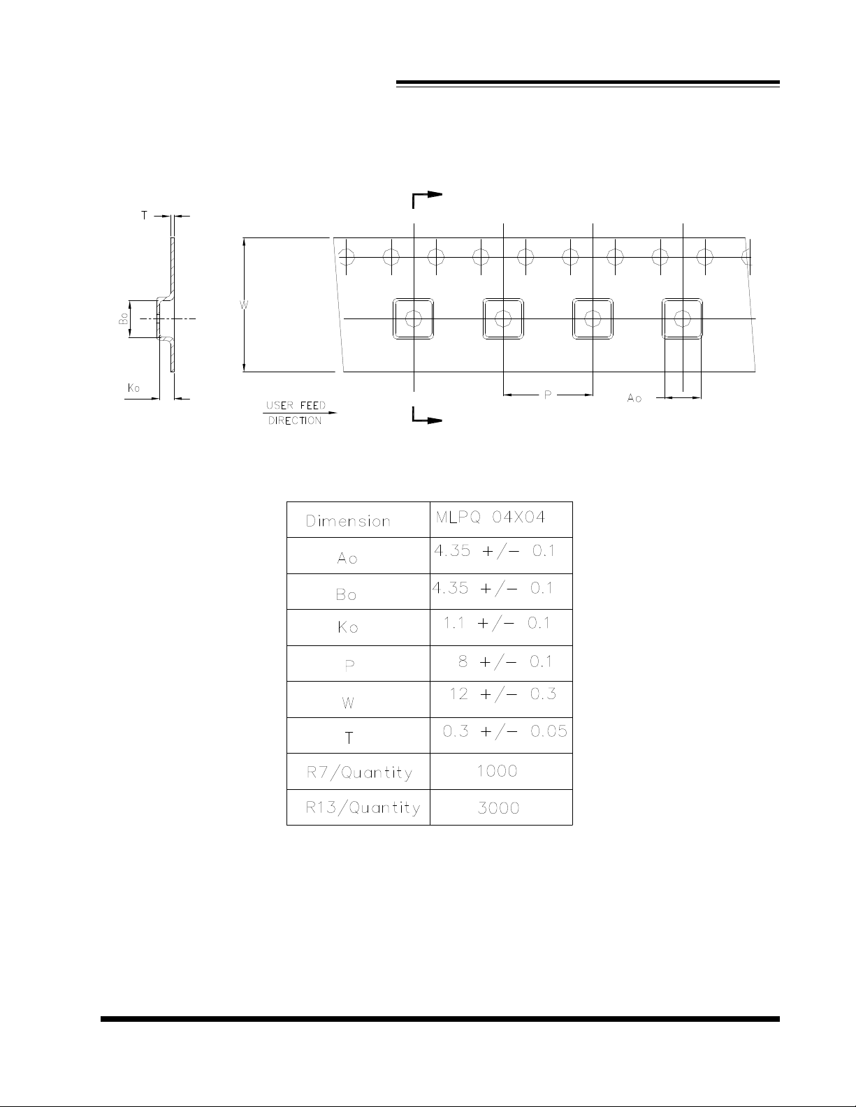
MLPQ 24 PIN 4 x 4 TAPE AND REEL INFORMATION
NX2420
Rev.1.9
05/06/08
NOTE:
1. R7 = 7 INCH LOCK REEL, R13 = 13 INCH LOCK REEL.
2. ALL DIMENSIONS ARE DISPLAYED IN MILLIMETERS.
www.nexsem.com
23
 Loading...